JP2004146541A - Light emitting element and method of manufacturing same - Google Patents
Light emitting element and method of manufacturing same Download PDFInfo
- Publication number
- JP2004146541A JP2004146541A JP2002308989A JP2002308989A JP2004146541A JP 2004146541 A JP2004146541 A JP 2004146541A JP 2002308989 A JP2002308989 A JP 2002308989A JP 2002308989 A JP2002308989 A JP 2002308989A JP 2004146541 A JP2004146541 A JP 2004146541A
- Authority
- JP
- Japan
- Prior art keywords
- layer
- light emitting
- substrate
- conductive oxide
- bonding
- Prior art date
- Legal status (The legal status is an assumption and is not a legal conclusion. Google has not performed a legal analysis and makes no representation as to the accuracy of the status listed.)
- Granted
Links
Images


Abstract
Description
【0001】
【発明の属する技術分野】
この発明は発光素子及び発光素子の製造方法に関する。
【0002】
【従来の技術】
【特許文献1】
特開2001−68731号公報
【0003】
(AlxGa1−x)yIn1−yP(ただし、0≦x≦1,0≦y≦1;以下、AlGaInPとも記載する)混晶により発光層部が形成された発光素子は、薄いAlGaInP活性層を、それよりもバンドギャップの大きいn型AlGaInPクラッド層とp型AlGaInPクラッド層とによりサンドイッチ状に挟んだダブルへテロ構造を採用することにより、高輝度の素子を実現できる。また、近年では、InxGayAl1−x−yN(ただし、0≦x≦1,0≦y≦1,x+y≦1;以下、InGaAlNとも記載する)を用いて同様のダブルへテロ構造を形成した青色発光素子も実用化されている。
【0004】
例えば、AlGaInP発光素子を例に取れば、n型GaAs基板上にヘテロ形成させる形にて、n型GaAsバッファ層、n型AlGaInPクラッド層、AlGaInP活性層、p型AlGaInPクラッド層をこの順序にて積層し、ダブルへテロ構造をなす発光層部を形成する。発光層部への通電は、素子表面に形成された金属電極を介して行なわれる。ここで、金属電極は遮光体として作用するため、例えば発光層部主表面の中央部のみを覆う形で形成され、その周囲の電極非形成領域から光を取り出すようにする。
【0005】
この場合、金属電極の面積をなるべく小さくしたほうが、電極の周囲に形成される光漏出領域の面積を大きくできるので、光取出し効率を向上させる観点において有利である。従来、電極形状の工夫により、素子内に効果的に電流を拡げて光取出量を増加させる試みがなされているが、この場合も電極面積の増大はいずれにしろ避けがたく、光漏出面積の減少により却って光取出量が制限されるジレンマに陥っている。また、クラッド層のドーパントのキャリア濃度ひいては導電率は、活性層内でのキャリアの発光再結合を最適化するために多少低めに抑えられており、面内方向には電流が広がりにくい傾向がある。これは、電極被覆領域に電流密度が集中し、光漏出領域における実質的な光取出量が低下してしまうことにつながる。そこで、クラッド層と電極との間に、キャリア濃度を高めた低抵抗率の電流拡散層を形成する方法が採用されている。電流拡散層は、電流拡散効果を十分なものとするために、少なくとも5μm〜10μm程度以上の厚みが必要とされ、有機金属気相成長法(MetalOrganic Vapor Phase Epitaxy:MOVPE法)や、液相エピタキシャル成長法(Liquid Phase Epitaxy:LPE法)により形成されている。
【0006】
他方、光取出し効率を向上させるために、発光層部の両面から光を取り出すことができるような素子構造が種々提案されている。AlGaInP発光素子の場合、発光層部の成長基板としてGaAs基板が使用されるが、GaAsはAlGaInP発光層部の発光波長域において光吸収が大きい。そこで、特許文献1には、発光層部の両面から光を取り出すために、一旦GaAs基板を剥離し、発光波長域において透明なGaP等の透明導電性基板を新たに貼り合わせる方法が開示されている。該公報においては、ITO(Indium Tin Oxide)等の導電性酸化物層を介して透明導電性基板を発光層部貼り合わせている。
【0007】
【発明が解決しようとする課題】
上記公報に開示された発光素子は、発光層部と透明導電性基板とを、それらの双方と接する導電性酸化物層により直接的に接合している。しかしながら、ITO等の導電性酸化物層は、発光層部あるいは透明導電性基板をなす化合物半導体とのコンタクト抵抗が高く、上記のような直接的な接合形態では、順方向の直列抵抗が高くなりすぎて、適正な動作電圧で駆動できなくなる問題がある。
【0008】
また、上記公報において、導電性酸化物層はITO微粒子を含むコロイダル溶液の塗付・焼付けにより形成しているが、このような方法で形成した導電性酸化物層は透明導電性基板に対する貼り合わせ力が小さく、剥離を起こしやすい問題がある。
【0009】
本発明の第一の課題は、厚い電流拡散層を有しているにもかかわらず、安価に製造可能であり、しかも直列抵抗が低く、低電圧にて十分な発光効率が得られる発光素子とその製造方法とを提供することにある。また、第二の課題は、電流拡散層の代わりとなる透明導電性半導体基板を発光層部に強固に結合できる発光素子の製造方法を提供することにある。
【0010】
【課題を解決するための手段及び作用・効果】
本発明の発光素子は、透明導電性半導体基板の一方の主表面上に化合物半導体よりなる発光層部が、導電性酸化物よりなる基板結合用導電性酸化物層を介して貼り合わされてなり、
発光層部と基板結合用導電性酸化物層との間に、該基板結合用導電性酸化物層の接合抵抗を減ずるためのコンタクト層が、該基板結合用導電性酸化物層に接するように配置されてなることを特徴とする。
【0011】
また、本発明の発光素子の製造方法の第一は、
透明導電性半導体基板の一方の主表面上に化合物半導体よりなる発光層部が、導電性酸化物よりなる基板結合用酸化物層を介して貼り合わされてなり、発光層部と基板結合用導電性酸化物層との間に、該基板結合用導電性酸化物層の接合抵抗を減ずるためのコンタクト層が、該基板結合用導電性酸化物層に接するように配置された発光素子を製造するために、
発光層成長用基板の第一主表面に、化合物半導体よりなる発光層部をエピタキシャル成長する発光層部成長工程と、
発光層部上に、基板結合用導電性酸化物層の接合抵抗を減ずるためのコンタクト層となるべき層を形成するコンタクト層形成工程と、
該発光層部及び/又は透明導電性半導体基板の貼り合わせ面側に、基板結合用導電性酸化物層を形成する基板結合用導電性酸化物層形成工程と、
発光層部と透明導電性半導体基板とを基板結合用導電性酸化物層を介して貼り合わせることにより、コンタクト層となるべき層が基板結合用導電性酸化物層に接するように配置された基板貼り合わせ体を作る貼り合わせ工程と、
発光層成長用基板を基板貼り合わせ体から剥離する剥離工程と、
を含むことを特徴とする。
【0012】
透明導電性半導体基板は、発光層部が発する光に対して透明な半導体にて構成される。なお、本明細書において「発光層部が発する光に対して透明」とは、発光層部が発する光の透過率が50%以上であることをいい、透過率50%未満を「発光層部が発する光に対して不透明」という。
【0013】
上記本発明によると、発光層成長用基板の第一主表面に、化合物半導体よりなる発光層部をエピタキシャル成長したあと、発光層部の、発光層成長用基板側とは反対側の主表面に、導電性酸化物層を介して透明導電性半導体基板を貼り合わせる。この透明導電性半導体基板を、例えば電流拡散層として利用する。その後、その基板貼り合わせ体から、発光層成長用基板を剥離する。導電性酸化物層は、発光層部との導通を良好に確保するための基板結合用導電性酸化物層として利用でき、また、発光層部と透明導電性半導体基板との格子整合も考慮する必要がないので、製造が容易である。また、十分な厚みを有した透明導電性半導体基板を発光層部に予め貼り合わせることにより、発光層部は発光層成長用基板の剥離に必要な機械的強度を十分に確保できる。また、電流拡散層となるべき部分を、MOVPE法やLPE法により厚く成長させるのではなく、透明導電性半導体基板の貼り合わせにより形成するので、コストアップ及び製造能率低下を生じにくい。
【0014】
他方、ITO等の導電性酸化物層は、化合物半導体層と直接接合しようとしたとき、良好なオーミック接合が必ずしも形成されず、接触抵抗に基づく直列抵抗増大により発光効率が低下することがある。しかしながら、基板結合用導電性酸化物層の接合抵抗を減ずるためのコンタクト層を、該基板結合用導電性酸化物層に接するように配置することで、前記接触抵抗を下げることができる。
【0015】
透明導電性半導体基板の非貼り合わせ側の主表面には、例えば、発光層部に対して電圧を印加するための金属電極を、該主表面の一部領域を覆う形で形成することができる。該透明導電性半導体基板は、光取出層あるいは電流拡散層として機能する。この場合、貼り合わせ工程の後、透明導電性半導体基板の非貼り合わせ側の主表面(以下、これを単に「主表面」ともいう)に、発光層部に対して電圧を印加するための金属電極を、該主表面の一部領域を覆う形で形成する電極形成工程を実施すればよい。
【0016】
基板結合用導電性酸化物層は、上記金属電極の直下領域からなる第一領域と残余の第二領域とを有するものとし、コンタクト層は、第二領域において、第一領域よりも形成面積率を大きくすることができる。なお、各領域のコンタクト層の形成面積率とは、領域中のコンタクト層の合計面積を、領域の全面積により割った比率をいう。該構成によると、光取り出し量が少ない金属電極の直下領域(第一領域)において、光取り出し量が多い残余の領域(第二領域)よりもコンタクト層の形成面積率を小さくしたから、第一領域における導電性酸化物層の接触抵抗が増大する。その結果、発光素子の駆動電流は、第一領域を迂回して第二領域に流れる成分が大きくなり、光取出効率を大幅に高めることができる。
【0017】
また、発光層部の、前記透明導電性半導体基板に面しているのと反対側の主表面は、透明電極を兼ねた電極用導電性酸化物層により覆うことができる。後述するITOなどの電極用導電性酸化物層は、GaP等の透明導電性半導体基板よりも電流拡散効果に優れ、また光透過性も良好であるから、この面を光取出面として活用することが、発光強度を高める上でより効果的である。電極用導電性酸化物層は、p−n接合を有する発光層部のn型層側に形成しておくと、光取出向上効果がより顕著となる。
【0018】
この場合、上記電極用導電性酸化物層と発光層部との間にも、該導電性酸化物層の接合抵抗を減ずるためのコンタクト層を、該導電性酸化物層と接する形にて形成することができる。これにより、電極用導電性酸化物層の接触抵抗を低減することができる。この場合、電極用導電性酸化物層の一部を覆う形で金属電極を形成し、電極用導電性酸化物層の該金属電極の周囲領域を光取出面とする。
【0019】
上記電極用導電性酸化物層も、金属電極の直下領域からなる第一領域と残余の第二領域とを有するものとして構成でき、コンタクト層は、第二領域において、第一領域よりも形成面積率が大きくすることができる。これにより、第一領域を迂回して第二領域に流れる電流量が大きくなり、光取出効率を大幅に高めることができる。
【0020】
基板結合用導電性酸化物層又は電極用導電性酸化物層に前述の金属電極を形成し、その第二領域において、第一領域よりもコンタクト層の形成面積率を大きくする場合、光取り出し量が少ない第一領域にはなるべく発光駆動電流が流れないことが光取出効率向上の観点においては望ましい。従って、第一領域にはコンタクト層が可及的に形成されていないことが望ましい。
【0021】
なお、第二領域において、第一領域よりもコンタクト層の形成面積率を大きく設定する構成は、全てのコンタクト層について採用してもよいし、一部のコンタクト層についてのみ採用し、他のコンタクト層を、例えば基板結合用導電性酸化物層の全面に渡って形成する構成としてもよい。特に、発光層部に最も近いコンタクト層は、第二領域において、第一領域よりも形成面積率を大きく設定することにより、駆動電流を第二領域に迂回させる効果が特に顕著である。
【0022】
また、導電性酸化物層の接合界面のうち、発光層部からの光を外部へ取り出す量が多い第二領域において少なくとも、コンタクト層の形成領域と非形成領域とが混在してなることが望ましい。コンタクト層の形成領域は、より具体的には分散形成されてなることが好ましい。該構造によると、導電性酸化物層の接触抵抗低減のために形成するコンタクト層が、発光層部からの光を吸収しやすい性質を有している場合においても、コンタクト層の形成領域直下にて発生した光は、これと隣接する非形成領域から漏出することにより、コンタクト層による吸収を抑制することができる。その結果、素子全体としての光取出効率を高めることができる。
【0023】
次に、透明導電性半導体基板と基板結合用導電性酸化物層との間にも、該基板結合用導電性酸化物層の接合抵抗を減ずるためのコンタクト層を、該基板結合用導電性酸化物層に接するように配置することができる。これにより、導電性酸化物層の接触抵抗をさらに減ずることができる。
【0024】
なお、発光層部の剥離側主表面は、電極用導電性酸化物層を形成する以外に、発光層成長用基板へのエピタキシャル成長により化合物半導体よりなる電流拡散層をあらかじめ形成しておき、その電流拡散層を素子側に残す形で発光層成長用基板を剥離する方法もある。この場合、形成する電流拡散層は、発光層成長用基板への成長初期段階で形成されるので、基板との格子整合条件が必然的に厳しくなり、制約が多い。例えば、GaAs基板を用いる場合は、これに格子整合可能な電流拡散層用の化合物半導体は、AlGaAsが数少ない候補となりうる。しかし、AlGaAsはバンドギャップエネルギーが比較的小さく、光吸収の問題が生じやすい(特に、560nm前後の黄緑色の発光波長)。また、Alを含有しているために、以降の発光層をエピタキシャル成長する際に高温酸化の問題も生じやすい。さらに、AlGaAs層をエピタキシャル成長するには高価なMOVPE法による成長工程が増える難点もある。しかしながら、後工程により電極用導電性酸化物層を形成する方法を採用すれば、基板への格子整合等は全く考慮する必要がなくなり、光吸収の問題もほとんど生じない。さらに、層成長も後述のスパッタリングなどの安価な方法が採用可能であり、しかも比較的低温での成長が可能であることから、発光層側の化合物半導体を酸化したりする心配も少ない。
【0025】
他方、上記電極用導電性酸化物層を形成する方法よりは、若干面倒な工程となるが、発光層部の両主表面に、導電性酸化物よりなる基板結合用導電性酸化物層を介して透明導電性半導体基板を貼り合わせる構成を採用することもできる。この構成によっても、発光層部の両面から光を効率的に取り出すことが可能となる。この場合、直列抵抗低減の観点から、前述のコンタクト層を各基板結合用導電性酸化物層と接して形成しておくことが望ましい。また、発光層部の剥離側主表面には、金属層を形成して、発光層部からの光を該金属層にて反射し、その反射光を、発光層部からの直接光に重畳させて取り出すこともできる。
【0026】
導電性酸化物層は、具体的には、ITOにて構成できる。ITOは、酸化スズをドープした酸化インジウム膜であり、酸化スズの含有量を1〜9質量%とすることで、電極層の抵抗率を5×10⁻⁴Ω・cm以下の十分低い値とすることができる。なお、ITO電極層以外では、ZnO電極層が高導電率であり、本発明に採用可能である。また、酸化アンチモンをドープした酸化スズ(いわゆるネサ)、Cd2SnO4、Zn2SnO4、ZnSnO3、MgIn2O4、酸化イットリウム(Y)をドープしたCdSb2O6、酸化スズをドープしたGaInO3なども導電性酸化物層の材質として使用することができる。すなわち、基板結合用導電性酸化物層はインジウム、スズ、亜鉛のいずれかを含むものとすることができる。これらの導電性酸化物は可視光に対して良好な透過性を有し(つまり、透明であり)、発光層部への電圧印加用電極として用いる場合、光の取出しを妨げない利点がある。また、該導電性酸化物層上に形成されるボンディングパッドなどの金属電極を介して素子駆動用の電圧を印加したとき、電流を面内に広げて発光を均一化し高効率化する役割も担う。
【0027】
これらの導電性酸化物層は、公知の気相成膜法、例えば化学蒸着法(chemicalvapor deposition:CVD)あるいはスパッタリングや真空蒸着などの物理蒸着法(physical vapor deposition:PVD)、あるいは分子線エピタキシャル成長法(molecular beam epitaxy:MBE)にて形成することができる。例えば、ITO電極層やZnO電極層は高周波スパッタリング又は真空蒸着により製造でき、また、ネサ膜はCVD法により製造できる。また、これら気相成長法に代えて、ゾル−ゲル法など他の方法を用いて形成してもよい。しかし、後述のように、基板結合用導電性酸化物層は非晶質とすることが貼り合わせ強度向上の観点において有利であり、この場合は、スパッタリングを最も好適に採用できる。
【0028】
貼り合わせに使用する導電性酸化物層の厚みは、層厚方向の電気伝導を主体的に考えればよいので、直列抵抗の増加を招かぬよう薄く形成すること、例えば50nm以上200nm以下(具体例:100nm)に形成することが望ましい。他方、発光層部の主裏面側の電極に使用する導電性酸化物層の厚みは、面内方向の電流拡散を考慮して、これよりも多少厚く形成すること、例えば100nm以上500nm以下(具体例:200nm)に形成することが望ましい。
【0029】
透明導電性半導体基板は、発光層からの光に対する屈折率が4以下のものを使用することが望ましい。屈折率を上記のように小さくすることにより、透明導電性半導体基板を経て光を取出す場合に、光取出し面における全反射の臨界角度が小さくなり、光取出効率を向上させることができる。
【0030】
発光層部は、例えば、各々(AlxGa1−x)yIn1−yP(ただし、0≦x,y≦1かつx+y=1)混晶にて構成される第一導電型クラッド層、活性層及び第二導電型クラッド層が積層されたダブルへテロ構造を有するものとして構成できる。この場合、透明導電性半導体基板として、上記ダブルへテロ構造層を有する発光層部からの、緑色〜赤色の発光波長帯(550nm以上650nm以下)の光に対し、550nm以上650nm以下の波長帯の光に対する屈折率が3.5以下のものを用いると、全反射の臨界角度を大きくすることができ、発光素子の光取出効率を向上させることができる。このような透明導電性半導体基板としては、具体的にはGaP、ZnO、SiC及びAlGaAs(特にAlAsの混晶比が0.75以上)のいずれかが、導電性も良好であるので、本発明に好適に使用できる。
【0031】
次に、上記の各コンタクト層は、具体的には、導電性酸化物層との接合界面においてAlを含有せず、かつバンドギャップエネルギーが1.42eVより小さい化合物半導体からなるものを好適に採用することができる。このようなコンタクト層を用いることにより、良好なオーミックコンタクトが得られ、また、Al成分酸化による抵抗増加も生じにくい。具体的にはInを含有したGaAsをコンタクト層として用いることができる。コンタクト層を構成する化合物半導体は、導電性酸化物層との接合界面においてInxGa1−xAs(0<x≦1)となっていれば、所期の接触抵抗低減効果が得られる。
【0032】
この場合、コンタクト層形成工程において、コンタクト層となるべきGaAs層を形成し、さらに基板結合用導電性酸化物層をなすITO層を当該GaAs層と接するように形成した後、熱処理することにより、ITO層からGaAs層にInを拡散させて、コンタクト層を、Inを含有したGaAs層として形成することができる。この場合、得られる発光素子は、導電性酸化物層がITO層であり、コンタクト層が、透明導電性酸化物層との接合界面においてInxGa1−xAs(0<x≦1)であり、かつ厚さ方向におけるIn濃度分布が、ITO層から厚さ方向に遠ざかるにつれ連続的に減少するものものとされる。
【0033】
該方法においては、発光層部上あるいは透明導電性半導体基板など、コンタクト層を形成したい側にGaAs層をまず形成し、そのGaAs層と接するようにITO層を形成する。例えば発光層部側にコンタクト層を形成する場合は、例えば周知のMOVPE法にて、発光層部成長用基板上にまず発光層部をエピタキシャル成長し、さらに、その上(ただし、別の層が介在していてもよい)にGaAs層をエピタキシャル成長すればよい。同様に、透明導電性半導体基板側にコンタクト層を形成したい場合は、透明導電性半導体基板上にGaAs層をエピタキシャル成長すればよい。
【0034】
コンタクト層はInGaAsを直接エピタキシャル成長する方法を採用してもよいのであるが、上記の方法を採用すると、次のような利点がある。すなわち、GaAs層は、例えばAlGaInPよりなる発光層部やGaPよりなる透明導電性半導体基板と格子整合が極めて容易であり、InGaAsを直接エピタキシャル成長する場合と比較して、均質で連続性のよい膜を形成できる。そして、そのGaAs層上にITO層を形成した後、熱処理することにより、ITO層からGaAs層にInを拡散させてコンタクト層とする。このように熱処理して得られるInを含有したGaAsよりなるコンタクト層は、In含有量が過剰とならず、発光層部との格子不整合による、発光強度低下などの品質劣化を効果的に防止することができる。GaAs層と発光層部との格子整合は、発光層部が(AlxGa1−x)yIn1−yP(ただし、0≦x≦1,0.45≦y≦0.55)にて構成される場合に特に良好となるので、混晶比yを上記の範囲に設定して、発光層部(クラッド層あるいは活性層)を形成することが望ましいといえる。
【0035】
上記の熱処理は、コンタクト層の厚さ方向におけるIn濃度分布が、図3の▲1▼に示すように、ITO層から厚さ方向に遠ざかるにつれ連続的に減少するものとなるようにする(つまり、In濃度分布に傾斜をつける)ことが望ましい。こうした構造は、熱処理により、ITO側からコンタクト層側へInを拡散させることにより形成される。
【0036】
また、コンタクト層の厚さ方向におけるIn濃度分布を、ITO層から厚さ方向に遠ざかるにつれ連続的に減少するものとすることで、以下のような利点が生ずる。すなわち、例えばAlGaInPよりなる発光層部側、あるいはGaPよりなる透明導電性半導体基板側に形成されるコンタクト層の場合、発光層部側あるいは透明導電性半導体基板側でIn濃度分布が小さくなり、発光層部ないし透明導電性半導体基板との格子定数差を縮めることができ、ひいては、格子整合性をより高めることができる。ただし、熱処理温度が過度に高くなったり、あるいは熱処理時間が長大化すると、ITO層からのIn拡散が過度に進行して、図3の▲3▼に示すように、コンタクト層内のIn濃度分布が厚さ方向にほぼ一定の高い値を示すようになり、上記の効果は得られなくなる(なお、熱処理温度が過度に低くなったり、あるいは熱処理時間が過度に短時間化すると、図3の▲2▼に示すように、コンタクト層内のIn濃度が不足することにつながる)。
【0037】
この場合、図3において、コンタクト層の、ITO透明電極層との境界近傍におけるIn濃度をCAとし、これと反対側の境界近傍におけるIn濃度をCBとしたとき、CB/CAが0.8以下となるように調整することが望ましく、該形態のIn濃度分布が得られるように、前述の熱処理を行なうことが望ましい。CB/CAが0.8を超えると、In濃度分布傾斜による発光層部との格子整合性改善効果が十分に得られなくなる。なお、コンタクト層の厚さ方向の組成分布(InあるいはGa濃度分布)は、層を厚さ方向に徐々にエッチングしながら、二次イオン質量分析(Secondary Ion Mass Spectroscopy:SIMS)、オージェ電子分光分析(Auger Electron Spectroscopy)、X線光電子分光(X−ray Photoelectron Spectroscopy:XPS)などの周知の表面分析方法により測定することができる。
【0038】
コンタクト層のITO透明電極層との境界近傍におけるIn濃度は、InとGaとの合計濃度に対するInの原子比にて、0.1以上0.6以下とされることが望ましく、上記の熱処理もこのようなIn濃度が得られるように行なうことが望ましい。上記定義によるIn濃度が0.1未満になると、コンタクト層の接触抵抗低減効果が不十分となり、0.6を超えるとコンタクト層と発光層部との格子不整合による、発光強度低下などの品質劣化が甚だしくなる。なお、コンタクト層のITO透明電極層との境界近傍におけるIn濃度が、InとGaとの合計濃度に対するInの原子比にて、例えば前述の望ましい値(0.1以上0.6以下)を確保できるのであれば、コンタクト層の、ITO透明電極層に面しているのと反対側の境界近傍でのIn濃度CBがゼロとなっていること、つまり、図4に示すように、コンタクト層のITO透明電極層側にInGaAs層が形成され、反対側の部分がGaAs層となる構造となっていても差し支えない。
【0039】
ITOは、前述の通り酸化スズをドープした酸化インジウム膜であり、ITO層をGaAs層上に形成し、さらにこれを適正な温度範囲にて熱処理することにより、上記望ましいIn濃度を有したコンタクト層を形成する。この熱処理により、ITO層の電気抵抗率をさらに低減できる。熱処理は、600℃以上750℃以下にて行なうことが望ましい。熱処理温度が750℃を超えるとGaAs層へのInの拡散速度が大きくなりすぎ、コンタクト層中のIn濃度が過剰となりやすくなる。また、In濃度が飽和して、コンタクト層の厚さ方向に傾斜したIn濃度分布も得にくくなる。いずれも、コンタクト層と発光層部との格子整合が悪化することにつながる。また、GaAs層へのInの拡散が過度に進みすぎると、コンタクト層との接触部付近にてITO層のInが枯渇し、電極の電気抵抗値の上昇が避けがたくなる。さらに、熱処理温度が上記のように高温になりすぎると、ITOの酸素がGaAs層へ拡散して酸化が促進され、素子の直列抵抗が上昇しやすくなる。いずれも適正な電圧で発光素子を駆動できなくなる不具合につながる。また、熱処理温度が極端に高くなると、ITO透明電極層の導電率がかえって損なわれる場合がある。他方、熱処理温度が600℃未満になると、GaAs層へのInの拡散速度が小さくなりすぎ、接触抵抗を十分に低下させたコンタクト層を得るのに長時間を要するようになるので、製造能率の低下が甚だしくなる。
【0040】
また、熱処理時間は、5秒以上120秒以下の短時間に設定することが望ましい。熱処理時間が120秒以上になると、特に、熱処理温度が上限値に近い場合、GaAs層へのInの拡散量が過剰となりやすくなる(ただし、熱処理温度を低めに留める場合は、これよりも長い熱処理時間(例えば300秒程度まで)を採用することも可能である。他方、熱処理時間が5秒未満になると、GaAs層へのInの拡散量が不足し、接触抵抗を十分に低下させたコンタクト層が得にくくなる。
【0041】
また、コンタクト層の、導電性酸化物層に接しているのと反対側の主表面には、中間層を介して発光層部又は透明導電性半導体基板を結合することができる。該中間層は、発光層部又は透明導電性半導体基板とコンタクト層との中間のバンドギャップエネルギーを有する化合物半導体により構成される。
【0042】
ダブルへテロ構造の発光層部は、活性層へのキャリア閉じ込め効果を高めて内部量子効率を向上させるために、クラッド層と活性層との間の障壁高さを一定以上に高める必要がある。図5の模式バンド図(Ecは伝導帯底、Evは価電子帯頂の各エネルギーレベルを示す)に示すように、このようなクラッド層(例えばAlGaInP)にコンタクト層(例えばInGaAs)を直接接合すると、クラッド層とコンタクト層との間に、接合によるバンドの曲がりにより、比較的高いヘテロ障壁が形成される場合がある。この障壁高さΔEは、クラッド層とコンタクト層との間のバンド端不連続値が大きくなるほど高くなり、キャリアの移動、特に有効質量のより大きいホールの移動を妨げやすくなる。例えば金属電極を使用する場合は、クラッド層の全面を金属電極で覆うと光取出しができなくなるので、部分的な被覆となるように電極形成せざるを得ない。この場合、光取出し効率向上のため、電極の面内方向外側への電流拡散を何らかの形で促進しなければならない。例えば、金属電極の場合も、発光層部との間にGaAs等のコンタクト層が形成されることが多いが、金属電極の場合は、コンタクト層と発光層部との間に、ある程度高い障壁が形成された方が、障壁によるキャリアのせき止め効果により面内方向の電流拡散を促進できる利点がある。しかし、高い障壁形成のため、直列抵抗の増加は避け難い。
【0043】
これに対し、ITO透明電極層を用いる場合は、ITO透明電極層自体が非常に高い電流拡散能を有しているため、障壁によるキャリアのせき止め効果はほとんど考慮する必要がない。しかも、ITO透明電極層の採用により、光取出領域の面積は金属電極使用時と比較して大幅に増加している。そこで、図6に示すように、コンタクト層とクラッド層との間に、それらコンタクト層とクラッド層との中間のバンドギャップエネルギーを有する中間層を挿入すると、コンタクト層と中間層、及び中間層とクラッド層とのそれぞれはバンド端不連続値が小さくなるので、各々形成される障壁高さΔEも小さくなる。その結果、直列抵抗が軽減されて、低い駆動電圧にて十分に高い発光強度を達成することが可能となる。
【0044】
上記中間層を採用することによる効果は、ダブルへテロ構造の発光層部の中でも、特にコンタクト層をなすInを含有したGaAsとの格子整合性が比較的良好な(AlxGa1−x)yIn1−yP(ただし、0≦x≦1,0≦y≦1)にて発光層部を形成する場合に顕著である。この場合、発光層部と、コンタクト層との中間のバンドギャップエネルギーを有する中間層として、具体的には、AlGaAs層、GaInP層及びAlGaInP層(バンドギャップエネルギーがクラッド層より小さくなるように組成調整されたもの)の少なくとも一つを含むものを好適に採用することができ、例えばAlGaAs層を含むものとして形成することができる。また、これ以外の発光層部、例えば、InxGayAl1−x−yNからなるダブルへテロ構造の発光層部にも適用可能である。この場合、中間層は、例えばInGaAlN層(バンドギャップエネルギーがクラッド層より小さくなるように組成調整されたもの)を含むものが採用可能である。
【0045】
透明導電性半導体基板と発光層部との貼り合わせに使用する導電性酸化物層は、非晶質酸化物とすることができる。また、本発明の発光素子の製造方法の第二は、透明導電性半導体基板の一方の主表面上に化合物半導体よりなる発光層部が、導電性酸化物よりなる基板結合用導電性酸化物層を介して貼り合わされた発光素子を製造するために、
発光層成長用基板の第一主表面に、化合物半導体よりなる発光層部をエピタキシャル成長する発光層部成長工程と、
該発光層部及び/又は透明導電性半導体基板の貼り合わせ面側に、非晶質よりなる基板結合用導電性酸化物層をスパッタリングにより形成する基板結合用導電性酸化物層形成工程と、
発光層部と透明導電性半導体基板とを基板結合用導電性酸化物層を介して貼り合わせることにより、基板貼り合わせ体を作る貼り合わせ工程と、
発光層成長用基板を基板貼り合わせ体から剥離する剥離工程と、
を含むことを特徴とする。
【0046】
非晶質よりなる導電性酸化物層を介すると、熱拡散等による発光層部と透明導電性半導体基板との貼り合わせが容易になる。特に、透明導電性半導体基板の貼り合わせ側主表面と、発光層部の貼り合わせ側主表面とをそれぞれ非晶質よりなる導電性酸化層にて覆い、それら導電性酸化層同士を接合することにより、透明導電性半導体基板と発光層部との貼り合わせを行なうようにすれば、発光層部と透明導電性半導体基板とを、容易かつ強固に貼り合わせることができる。基板結合用導電性酸化物層を非晶質として形成する場合、基板温度の上昇しにくいスパッタリングの採用が有利である。
【0047】
【発明の実施の形態】
以下、本発明の実施の形態を添付の図面を参照して説明する。
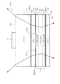
図1は、本発明の一実施形態である発光素子100を示す概念図である。発光素子100は、透明導電性半導体基板であるp−GaP単結晶基板7の主裏面MP2上に発光層部24が設けられている。該発光層部24の主裏面MP3の全面が、電極用透明導電性酸化物層であるITO層20により覆われている。p−GaP単結晶基板7は電流拡散層及び光取出層として機能し、その主表面MP1の略中央に、発光層部24に発光駆動電圧を印加するための金属電極(例えばAu電極)9が、前記主表面MP1の一部を覆うように形成されている。p−GaP単結晶基板7の主表面MP1における、金属電極9の周囲の領域は、発光層部24からの光取出領域をなす。また、発光層部24の主裏面MP3は、ITO層20を介して、その全面より光取出が可能である。
【0048】
発光層部24は、ノンドープ(AlxGa1−x)yIn1−yP(ただし、0≦x≦0.55,0.45≦y≦0.55)混晶からなる活性層5を、p型(AlzGa1−z)yIn1−yP(ただしx<z≦1)からなるp型クラッド層6(第一導電型クラッド層)とn型(AlzGa1−z)yIn1−yP(ただしx<z≦1)からなるn型クラッド層4(第二導電型クラッド層)とにより挟んだ構造を有し、活性層5の組成に応じて、発光波長を、緑色から赤色領域(発光波長(中心波長)が550nm以上650nm以下)にて調整できる。図1の発光素子100では、金属電極9側にp型AlGaInPクラッド層6が配置されており、ITO層20側にn型AlGaInPクラッド層4が配置されている。従って、通電極性は金属電極9側が正である。なお、ここでいう「ノンドープ」とは、「ドーパントの積極添加を行なわない」との意味であり、通常の製造工程上、不可避的に混入するドーパント成分の含有(例えば1013〜1016/cm3程度を上限とする)をも排除するものではない。
【0049】
p−GaP単結晶基板7は、例えばZnをp型ドーパントとして含有するp−GaP単結晶インゴットをスライス・研磨して製造されたものであり、その厚みは例えば100μm以上500μm以下である。また、発光層部24からの波長550nm以上650nm以下の光に対しての屈折率が3.35程度である。そして、発光層部24の主表面MP4に対し、基板結合用導電性酸化物層をなすITO層10を介して貼り合わされている。ITO層20及び10はいずれも非晶質である。
【0050】
また、発光層部24と接するITO層10,20の発光層部24との接触側、あるいはp−GaP単結晶基板7との接触側に、InGaAs等よりなるコンタクト層30が、それらITO層10,20と接して形成されている。コンタクト層30は、光吸収の影響を小さくするため、その厚さを1nm以上20nm以下(望ましくは5nm以上10nm以下)とする。
【0051】
なお、各コンタクト層30と、発光層部24との間あるいはp−GaP単結晶基板7との間には、それらコンタクト層と発光層部24(クラッド層)あるいはp−GaP単結晶基板7との中間のバンドギャップエネルギーを有する中間層31を形成している。該中間層31は、例えばAlGaAs、GaInP及びAlGaInPの少なくとも1つを含むものとして構成できる。本実施形態では、各中間層31の全体を単一のAlGaAs層として構成している。
【0052】
また、基板結合用導電性酸化物層をなすITO層10については、発光層部24に近い側のコンタクト層30が、金属電極9の直下領域をなす光取り出し量が少ない第一領域PAには形成されず、その周囲の光取り出し量が多い第二領域SAにのみ選択的に形成されている。これにより、第一領域PAでの直列抵抗が選択的に高められる結果、第二領域SA、すなわち金属電極9の周囲への迂回電流密度が増加し、光取出し効率が高められる。このようなコンタクト層30は、第一領域PAにおいて非形成となるように、周知のフォトリソグラフィー技術を用いてパターニングすることにより形成できる。
【0053】
なお、本実施形態では、ITO層10のp−GaP単結晶基板7側のコンタクト層30、あるいは発光層部24の裏面側のITO層20のコンタクト層30については、ITO層10ないし20の全面を覆うように形成している。しかし、これらのコンタクト層30についても、同様に、第二領域SAにのみ選択的に形成する構成を採用することができ、これにより、さらに光取出し効率を高めることが可能である。また、中間層31については、コンタクト層30に対応させてパターニングしてもよいし、中間層31はITO層10の全面に形成し、コンタクト層30のみパターニングすることも可能である。
【0054】
なお、ITO層10のp−GaP単結晶基板7側のコンタクト層30は、図7(a)〜(c)に示すように、第二領域SAにおいて、形成領域と非形成領域とを混在させた形とすることもできる。この場合、コンタクト層30の非形成領域においてはITO層10が発光層部24と直接接触する形となる。コンタクト層30の形成領域は、ITO層10の接合界面において分散形成することにより、発光層部24における発光をより均一化し、かつコンタクト層30の非形成領域からより均一に光を取り出すことができる。図7(a)はコンタクト層30の形成領域を散点状とした例であり、(b)は細長い帯状のコンタクト層30の形成領域と、同形態の非形成領域とを交互に形成した例である。さらに、(c)は、(a)とは逆に、コンタクト層30の形成領域を背景として、散点状の非形成領域をこれに分散形成した例である。ここではコンタクト層30の形成領域を格子状に形成している。なお、図1の他のコンタクト層30についても、同様に、形成領域と非形成領域とを混在させた形とすることができる。また、中間層31は、コンタクト層30に対応させてパターニングしてもよいし、コンタクト層30のみパターニングすることも可能である。該パターニングは周知のフォトリソグラフィー技術により行なうことができる。以上の構造は、後述の図12の素子形態において、電極用導電性酸化物層をなすITO層20を、コンタクト層30を介して設ける場合、当該コンタクト層30についても全く同様に適用でき、同様の作用・効果を達成できる。
【0055】
以下、図1の発光素子100の製造方法について説明する。
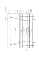
まず、図2の工程1に示すように、発光層成長用基板をなす半導体単結晶基板であるGaAs単結晶基板1の主表面MP5に、n型GaAsバッファ層2を例えば0.5μm、さらにAlAsからなる剥離層3を例えば0.5μmエピタキシャル成長させる。次いで、後にコンタクト層30となるGaAs層30’と中間層31とをこの順序でエピタキシャル成長させ、さらに発光層部24として、1μmのn型AlGaInPクラッド層4、0.6μmのAlGaInP活性層(ノンドープ)5、及び1μmのp型AlGaInPクラッド層6を、この順序にエピタキシャル成長させる。さらに、そのp型AlGaInPクラッド層6上に、同様の中間層31とGaAs層30’とをこの順序でエピタキシャル成長させる。なお、最後の中間層31及びGaAs層30’はフォトリソグラフィーにより、金属電極9(図1)に対応する領域(第一領域)だけ、非形成とする。
【0056】
中間層31及びGaAs層30’も、基本的にはMOVPE法等により形成することができる。特にGaAs層30’については、Inを含有したITO層10あるいは20と接して形成することを考慮して、以下のような工程を採用する。すなわち、図2の工程1にて、p型クラッド層6上に中間層31を、次いでGaAs層30’をMOVPE法等により形成した後、ITO層10aを形成する。工程3及び工程6においても、p−GaP単結晶基板7とn型クラッド層4上にそれぞれ中間層31及びGaAs層30’を形成してから、各ITO層10b及び20を形成する。そして、ITO層10aと10bとを貼り合せにより一体化してITO層10とし、この状態で高温で短時間の熱処理を行なうことにより、各ITO層10及び20から、対応するGaAs層30’へInを拡散させる。以下、具体的に説明する。
【0057】
まず、工程2に示すように、発光層部24の主表面MP4に、透明導電酸化物層としてITO層10aを、高周波スパッタリングを用いて形成する。他方、工程3に示すように、別途用意したp−GaP単結晶基板7の主裏面MP2にも同様のITO層10bを形成する。そして、p−GaP単結晶基板7のITO層10bを、発光層部24のITO層10aに重ね合わせて圧迫し、工程4に示すように、所定の条件(例えば450℃にて30分間)にて熱処理することにより、基板貼り合わせ体50を作る。ITO層10aとITO層10bとは一体化して基板結合用導電性酸化物層10となる。
【0058】
次に、工程5に進み、上記基板貼り合わせ体50を、例えば10%フッ酸水溶液からなるエッチング液に浸漬し、バッファ層2と発光層24との間に形成した前記AlAs剥離層3を選択エッチングすることにより、GaAs単結晶基板1(発光層24からの光に対して不透明である)を、発光層部24とこれに接合されたp−GaP単結晶基板7との積層体50aから剥離する。なお、AlAs剥離層3に代えてAlInPよりなるエッチストップ層を形成しておき、GaAsに対して選択エッチング性を有する第一エッチング液(例えばアンモニア/過酸化水素混合液)を用いてGaAs単結晶基板1をGaAsバッファ層2とともにエッチング除去し、次いでAlInPに対して選択エッチング性を有する第二エッチング液(例えば塩酸:Al酸化層除去用にフッ酸を添加してもよい)を用いてエッチストップ層をエッチング除去する工程を採用することもできる。
【0059】
次に、工程6に示すように、GaAs単結晶基板1の剥離により露出した発光層24の、主裏面MP3上に形成された中間層31及びGaAs層30’を覆うように、ITO層20を形成する。こうして得られた積層体ウェーハ(電極9の形成前であっても形成後であってもいずれでもよい)を炉の中に配置し、例えば窒素雰囲気中あるいはAr等の不活性ガス雰囲気中にて、600℃以上750℃以下(例えば700℃)の低温で、5秒以上120秒以下(例えば30秒)の短時間の熱処理を施す。これにより、各ITO層10,20からGaAs層30’にInが拡散し、Inを含有したGaAsよりなるコンタクト層30(図1等)が得られる。なお、この熱処理は、GaAs層とこれを覆うITO層とを形成する毎にその都度行なうことも可能であるが、上記のように、全てのITO層の形成が終わったあとで一括して行なうと、工程が簡略化されるのでより有利であり、また、順次的な熱処理により、先に形成されたGaAs層30’ほどIn拡散が累積されて過剰となる不具合も生じない。
【0060】
該コンタクト層30は、図3▲1▼において、ITO透明電極層との界面近傍におけるIn濃度が、InとGaとの合計濃度に対するInの原子比にて、0.1以上0.6以下とされる。また、In濃度は、ITO層から厚さ方向に遠ざかるにつれ連続的に減少するものとなっており、ITO層との各境界近傍におけるIn濃度をCAとし、これと反対側の境界近傍におけるIn濃度をCBとしたとき、CB/CAが0.8以下となるように調整されている。
【0061】
コンタクト層30は、AlGaInPよりなる発光層部24やp−GaP基板7との格子整合性の良好なGaAs層30’をまず形成し、さらにITO層を形成した後、比較的低温で短時間の熱処理を施すことにより、In含有量が過剰でなく、しかも均質で連続性の良好なものとなる。その結果、格子不整合による、発光強度低下などの品質劣化を効果的に防止することができる。以下、通常の方法によりダイシングして半導体チップとし、これを支持体に固着してリード線のワイヤボンディング等を行なった後、樹脂封止をすることにより最終的な発光素子が得られる。
【0062】
なお、この最後に形成されるITO層20は、裏面側の電極として用いられ、導電性酸化物であるITOにて構成されることで、光取出機能と電流拡散機能とを実現する。電流拡散機能を高めるには、ITO層20のシート抵抗(あるいは電気比抵抗)を低減することが重要であり、また、光取出機能を高めるには、必要に応じてITO層20を厚く形成した場合でも、十分な光透過性が確保できるようにすることが重要である。例えばITO層20をスパッタリングにより形成する場合、シート抵抗を低減するには、スパッタリング電圧をなるべく低く設定することが望ましい。これは、スパッタリングのプラズマ中に含まれる負イオン(主に酸素イオンである)が堆積中のITO層に高速で入射すると、絶縁性のInOが形成されやすくなるが、加速電圧が低くなると該InOの形成が抑制されるためである。このようなスパッタリングの低電圧化を図るためには、スパッタリング時の磁界強度を一定以上に高めること(例えば、0.8kG以上:電圧低減効果が飽和するので2000G以下で設定することが望ましい)が有効である。シート抵抗の低減は、例えばカソード電圧の絶対値にて350V以下、望ましくは250V以下に設定することで顕著となる。磁界強度を例えば1000G以上に設定すれば、スパッタリング電圧をカソード電圧の絶対値にて250V以下に容易に調整することができる。
【0063】
均質で光透過率の高いITO層を得るには、また、発光層部と透明導電性半導体基板とを容易かつ強固に貼り合わせるためには、ITO層を、明確な結晶粒界が形成されない非晶質層とすることが有利である。非晶質のITO層を得るには、ITOの結晶化を防止するため200℃以下の低温で成膜を行なう必要がある。この場合、低抵抗のITO層を得るために、上記のスパッタリング条件と組み合わせることが有効であり、特に、低温でも均質で低抵抗率のITO層を得るには、スパッタリング雰囲気中に水蒸気を導入することが有効である(例えば3×10⁻³Pa以上15×10−3Pa以下)。スパッタリング雰囲気の水蒸気分圧が過度に低くなると、得られるITO層の微結晶化が進みやすくなり、光透過率の低下及びシート抵抗の上昇が著しくなるが、一定以上の水蒸気分圧を確保することで、この微結晶化を効果的に抑制することができる。これにより、光透過率が90%以上(望ましくは95%以上)、比抵抗が1000μΩ・cm以下(望ましくは800μΩ・cm以下)のITO層を実現できるようになる。
【0064】
また、ITO層20は、均一で大きな電流拡散効果を有していることが、均一で高い発光効率を実現する上で重要である。そのためには、ITO層を均質で低抵抗率のものとして構成する以外に、その表面の平滑性を高めることが必要となる。表面の平滑性が低下すると、電界集中しやすい突起部が多数形成されやすくなり、発光層部24への印加電圧の不均一化により局所的な暗所を生じやすくなったり、あるいはリーク電流の発生により発光効率そのものが低下することにつながる。これらの不具合防止のため、ITO層の表面粗さは、具体的には、原子間力顕微鏡(AFM)による3次元表面トポグラフィーにて、評価面積を0.2μm四方としたときのRmaxの値にて10nm以下とすること(例えば4nm以上7nm以下)に設定することが望ましい。
【0065】
上記のようなITO層の表面平滑化のためには、ITO層を形成したあと、その表面を研磨することが有効であるが、機械的な研磨は高コストなので化学研磨の採用が望ましい。ITOの化学研磨液としては、例えば塩酸と硝酸の混合液や、蓚酸水溶液をを採用できる。この場合、前述のようなITO層の微結晶化が進むと、結晶粒界でエッチングが進行しやすいことから、粒界侵食や脱粒による表面粗化を生じやすくなる。従って、均質な非晶質層を得るために、スパッタリング雰囲気中への水蒸気を導入することは、化学研磨後のITO層の表面粗さを上記のように低減する上でも有力な手法となりうる。
【0066】
例えば、大面積の面発光型素子(例えば、1辺が300μm)の発光強度を最大限に高めるためには、大面積のITO層にできるだけ大きな電流を均一に流すことが重要である。従って、大面積の面発光型素子に本発明を適用する場合には、上記のように平滑かつ低抵抗率であり、かつ、光透過率の高いITO層を採用することが特に有利であるといえる。
【0067】
図1において、発光層部24側のコンタクト層30は、適当なドーパントの添加により、これと接するクラッド層6ないし4とそれぞれ同じ導電型を有するものとして形成してもよいが、これらコンタクト層30を上記のような薄層として形成する場合は、これらをドーパント濃度の低い低ドープ層(例えば1017個/cm3以下;あるいはノンドープ層(1013個/cm3〜1016個/cm3))として形成しても直列抵抗の過度の増加を招かないので、問題なく採用可能である。他方、低ドープ層とした場合、発光素子の駆動電圧によっては、以下のような効果が達成できる。すなわち、コンタクト層30を低ドープ層とすることで、層の電気抵抗率自体は高くなるので、これを挟む電気抵抗率の小さいクラッド層あるいはITO層10,20に対して、コンタクト層30の層厚方向に印加される電界(すなわち、単位距離当たりの電圧)が相対的に高くなる。このとき、コンタクト層30を、バンドギャップの比較的小さいInを含有したGaAsにより形成しておくと、上記電界の印加によりコンタクト層のバンド構造に適度な曲がりが生じ、より良好なオーミック状接合を形成することができる。そして、図3に示すように、コンタクト層30のIn濃度が、ITO層10,20との接触側にて高められていることで、該効果が一層顕著なものとなる。
【0068】
なお、図8に示す発光素子200のように、ITO層20の主裏面MP6を、Au等の金属反射層21にて覆うこともできる。この構成によると、発光層部24から主裏面側に放出される光が金属反射層21にて反射され、その反射光が、発光層部24からp−GaP単結晶基板7側に直接放出される光に重畳されるので、該側における発光強度を大幅に高めることができる。また、図9に示す発光素子300のように、p−GaP単結晶基板7の主表面MP1の全面を、電極を兼ねた金属反射層21により覆い、その金属反射層21による反射光と、発光層部24から主裏面側に直接放出される光とを重畳させて、ITO層20側から取り出すこともできる。
【0069】
また、図10に示すように、工程1〜5までを図2と同様に実施し、GaAs基板1を剥離した後、工程7に示すように、発光層部24の主裏面MP3側に別の透明導電性半導体基板であるGaP単結晶基板23(本実施形態ではn型)を貼り合わせることもできる。具体的には、発光層部24の主裏面MP3にITO層20aを、GaP単結晶基板23の主表面MP7にITO層20bを、それぞれ中間層31及びGaAs層30’を介して形成し、工程3及び工程4と同様に熱処理により貼り合わせを行なう。貼り合わせ後、例えば図11に示すように、GaP単結晶基板23の金属電極層21を形成し、発光素子400とすることができる。
【0070】
また、図12に示す発光素子500は、発光層部24の、透明導電性半導体基板23に面しているのと反対側の主表面を、透明電極を兼ねた電極用導電性酸化物層20にて覆っているが、該電極用導電性酸化物層20の一部を覆う形で金属電極9が形成されてなり、電極用導電性酸化物層20の該金属電極9の周囲領域を光取出面として利用している。透明導電性半導体基板23はn−GaP単結晶基板23であり、電極用導電性酸化物層20はITO層20である。n−GaP単結晶基板23は、図1の発光素子100と同様、基板結合用導電性酸化物層をなすITO層10(両面にコンタクト層30及び中間層31が、ITO層10の側からこの順序で形成されている)を介して、発光層部24のn型クラッド層4側に貼り合わせてある。また、n−GaP単結晶基板23の裏面は、全面が反射層を兼ねた金属電極21(例えばAu電極)により覆われている。他方、ITO層20とp型クラッド層6との間には、ITO層20側から、コンタクト層30及び中間層31がこの順序で形成されている。コンタクト層30は、金属電極16の直下領域をなす光取り出し量が少ない第一領域PAには形成されず、その周囲の光取り出し量が多い第二領域SAにのみ選択的に形成されている。これらコンタクト層30及び中間層31の組成及び厚さは、図1の発光素子にて、p型クラッド層6に接して形成されているコンタクト層30及び中間層31と同じであり、図7と同様の形態でパターンニングが可能である(中間層31のパターニングについては、図1の素子と同様に省略してもよい)。
【0071】
上記素子の製法の一例を図13に示す(特に断りのない部分については、図2と同様の工程が採用可能である)。工程1は、図2の工程1と略同じであるが、p型GaAs基板1を用い、その上に発光層部24をなすp型クラッド層6、活性層5及びn型クラッド層4を、図2とは逆順に形成する。次に、工程2においては、n−GaP単結晶基板23の片側の主表面に、中間層31とGaAs層30’とをこの順序で形成し、さらにITO層10bを形成したものを用意する。また、発光層部24のn型クラッド層4側のGaAs層30’上にもITO層10aを形成する。そして、n−GaP単結晶基板23のITO層10bを、発光層部24のITO層10aに重ね合わせて圧迫し、所定の条件(例えば450℃にて30分間)にて熱処理することにより、貼り合わせを行なう(工程3)。そして、工程4においてGaAs基板1を剥離し、工程5では、露出したGaAs層30’を、フォトリソグラフィーにより、第一領域を除去する形でパターニングする。そして、工程6に示すように、そのパターニングされたGaAs層30’上にITO層20を形成し、さらに、前述のIn拡散のための短時間の熱処理を行なう。その後、電極9及び21を形成する。
【0072】
以上説明した実施形態では、発光層部24の各層をAlGaInP混晶にて形成していたが、該各層(p型クラッド層6、活性層5及びn型クラッド層4)をAlGaInN混晶により形成することにより、青色あるいは紫外発光用のワイドギャップ型発光素子を構成することもできる。発光層部24は、図1の発光素子100と同様にMOVPE法により形成される。この場合、発光層部24を成長させるための発光層成長用基板をなす半導体単結晶基板は、GaAs単結晶基板に代えて、例えばサファイア基板(絶縁体)が使用される。
【0073】
さらに、活性層5は上記実施形態では単一層として形成していたが、これを、バンドギャップエネルギーの異なる複数の化合物半導体層が積層されたもの、具体的には、量子井戸構造を有するものとして構成することもできる。量子井戸構造を有する活性層は、混晶比の調整によりバンドギャップが互いに相違する2層、すなわちバンドギャップエネルギーの小さい井戸層と大きい障壁層とを、各々電子の平均自由工程もしくはそれ以下の厚さ(一般に、1原子層〜数nm)となるように格子整合させる形で積層したものである。上記構造では、井戸層の電子(あるいはホール)のエネルギーが量子化されるため、例えば半導体レーザー等に適用した場合に、発振波長をエネルギー井戸層の幅や深さにより自由に調整でき、また、発振波長の安定化、発光効率の向上、さらには発振しきい電流密度の低減などに効果がある。さらに、井戸層と障壁層とは厚さが非常に小さいため、2〜3%程度までであれば格子定数のずれが許容され、発振波長領域の拡大も容易である。なお、量子井戸構造は、井戸層を複数有する多重量子井戸構造としてもよいし、井戸層を1層のみ有する単一量子井戸構造としてもいずれでもよい。なお、障壁層の厚さは、例えばクラッド層と接するもののみ50nm程度とし、他は6nm程度とすることができる。また、井戸層は5nm程度とすることができる。
【図面の簡単な説明】
【図1】本発明の発光素子の第一実施形態を積層構造にて示す模式図。
【図2】図1の発光素子の製造工程を示す説明図。
【図3】コンタクト層のIn濃度分布の一例を示す概念図。
【図4】コンタクト層のIn濃度分布の変形例を示す概念図。
【図5】中間層を形成しない場合の、コンタクト層のバンド構造の例を示す模式図。
【図6】中間層を形成する場合の、コンタクト層のバンド構造の例を示す模式図。
【図7】図1の発光素子の、コンタクト層の種々のパターニング形態を示す模式図。
【図8】本発明の発光素子の第二実施形態を積層構造にて示す模式図。
【図9】本発明の発光素子の第三実施形態を積層構造にて示す模式図。
【図10】図2の製造工程の第一変形例を示す説明図。
【図11】本発明の発光素子の第四実施形態を積層構造にて示す模式図。
【図12】本発明の発光素子の第五実施形態を積層構造にて示す模式図。
【図13】図12の発光素子の製造方法の一例を示す工程説明図。
【符号の説明】
1 GaAs単結晶基板(発光層成長用基板)
4 n型クラッド層(第二導電型クラッド層)
5 活性層
6 p型クラッド層(第一導電型クラッド層)
7,23 GaP単結晶基板(透明導電性半導体基板)
9 金属電極
10 ITO層(基板結合用導電性酸化物層)
20 ITO層(導電性酸化物層)
24 発光層部
30 コンタクト層
30’ GaAs層
31 中間層
100,200,300,400,500 発光素子[0001]
TECHNICAL FIELD OF THE INVENTION
The present invention relates to a light emitting device and a method for manufacturing the light emitting device.
[0002]
[Prior art]
[Patent Document 1]
JP 2001-68731 A
[0003]
(Al x Ga 1-x ) y In 1-y A light emitting element having a light emitting layer portion formed by a mixed crystal of P (0 ≦ x ≦ 1, 0 ≦ y ≦ 1; hereinafter also referred to as AlGaInP) has a thin AlGaInP active layer and a band gap larger than that. By employing a double hetero structure sandwiched between an n-type AlGaInP cladding layer and a p-type AlGaInP cladding layer, a high-luminance element can be realized. In recent years, In x Ga y Al 1-xy A blue light-emitting element using N (where 0 ≦ x ≦ 1, 0 ≦ y ≦ 1, x + y ≦ 1; hereinafter also referred to as InGaAlN) to form a similar double heterostructure has been put to practical use.
[0004]
For example, taking an AlGaInP light emitting device as an example, an n-type GaAs buffer layer, an n-type AlGaInP cladding layer, an AlGaInP active layer, and a p-type AlGaInP cladding layer are formed in this order in a hetero-form on an n-type GaAs substrate. The layers are stacked to form a light emitting layer portion having a double hetero structure. Electric current is applied to the light emitting layer via a metal electrode formed on the element surface. Here, since the metal electrode functions as a light shield, it is formed, for example, so as to cover only the central portion of the main surface of the light emitting layer portion, and light is extracted from the surrounding electrode non-formed region.
[0005]
In this case, reducing the area of the metal electrode as much as possible is advantageous from the viewpoint of improving the light extraction efficiency because the area of the light leakage region formed around the electrode can be increased. Conventionally, attempts have been made to increase the amount of light taken out by effectively spreading the current in the device by devising the shape of the electrodes.In this case, however, it is unavoidable to increase the electrode area anyway, and the light leakage area is increased. The decrease has led to the dilemma of limiting the amount of light extraction. In addition, the carrier concentration of the dopant in the cladding layer, and consequently, the electrical conductivity, are suppressed somewhat lower in order to optimize the radiative recombination of the carriers in the active layer, and the current tends to hardly spread in the in-plane direction. . This causes the current density to concentrate in the electrode coating region, leading to a substantial decrease in light extraction in the light leakage region. Therefore, a method of forming a low-resistivity current diffusion layer having an increased carrier concentration between the cladding layer and the electrode has been adopted. The current diffusion layer is required to have a thickness of at least about 5 μm to 10 μm in order to make the current diffusion effect sufficient, and a metal organic vapor phase epitaxy (MOVPE) method or a liquid phase epitaxial growth method It is formed by a method (Liquid Phase Epitaxy: LPE method).
[0006]
On the other hand, in order to improve light extraction efficiency, various element structures capable of extracting light from both surfaces of a light emitting layer have been proposed. In the case of an AlGaInP light-emitting element, a GaAs substrate is used as a growth substrate for the light-emitting layer, and GaAs has a large light absorption in the emission wavelength region of the AlGaInP light-emitting layer. Therefore,
[0007]
[Problems to be solved by the invention]
In the light-emitting element disclosed in the above publication, the light-emitting layer portion and the transparent conductive substrate are directly joined by a conductive oxide layer in contact with both of them. However, a conductive oxide layer such as ITO has a high contact resistance with the light emitting layer portion or the compound semiconductor forming the transparent conductive substrate, and the direct junction form as described above has a high forward series resistance. There is a problem that it is impossible to drive with an appropriate operating voltage.
[0008]
In the above publication, the conductive oxide layer is formed by applying and baking a colloidal solution containing ITO fine particles. The conductive oxide layer formed by such a method is bonded to a transparent conductive substrate. There is a problem that the force is small and peeling easily occurs.
[0009]
A first object of the present invention is to provide a light-emitting element that can be manufactured at low cost, has a low series resistance, and has sufficient luminous efficiency at a low voltage, despite having a thick current diffusion layer. And a method of manufacturing the same. Another object of the present invention is to provide a method for manufacturing a light-emitting device that can firmly couple a transparent conductive semiconductor substrate that substitutes for a current diffusion layer to a light-emitting layer portion.
[0010]
[Means for Solving the Problems and Functions / Effects]
The light-emitting element of the present invention has a light-emitting layer portion made of a compound semiconductor on one main surface of a transparent conductive semiconductor substrate, which is bonded via a substrate-binding conductive oxide layer made of a conductive oxide,
Between the light-emitting layer portion and the conductive oxide layer for bonding the substrate, a contact layer for reducing the junction resistance of the conductive oxide layer for bonding the substrate is in contact with the conductive oxide layer for bonding the substrate. It is characterized by being arranged.
[0011]
Further, the first of the method for manufacturing a light emitting device of the present invention,
A light-emitting layer portion made of a compound semiconductor is attached to one main surface of the transparent conductive semiconductor substrate via a substrate-binding oxide layer made of a conductive oxide, and the light-emitting layer portion and the substrate-bonding conductive layer are bonded together. To manufacture a light emitting element in which a contact layer for reducing the junction resistance of the conductive oxide layer for bonding to a substrate is arranged between the oxide layer and the oxide layer so as to be in contact with the conductive oxide layer for bonding a substrate. To
A light emitting layer portion growing step of epitaxially growing a light emitting layer portion made of a compound semiconductor on the first main surface of the light emitting layer growth substrate;
On the light emitting layer portion, a contact layer forming step of forming a layer to be a contact layer for reducing the junction resistance of the conductive oxide layer for substrate bonding,
A substrate-bonding conductive oxide layer forming step of forming a substrate-bonding conductive oxide layer on the bonding surface side of the light emitting layer portion and / or the transparent conductive semiconductor substrate;
A substrate in which a layer to be a contact layer is arranged so as to be in contact with the conductive oxide layer for bonding the substrate by bonding the light emitting layer portion and the transparent conductive semiconductor substrate via the conductive oxide layer for bonding the substrate. A bonding process for making a bonded body,
A peeling step of peeling the light emitting layer growth substrate from the bonded substrate,
It is characterized by including.
[0012]
The transparent conductive semiconductor substrate is formed of a semiconductor transparent to light emitted from the light emitting layer. In the present specification, “transparent to light emitted from the light emitting layer portion” means that the transmittance of the light emitted from the light emitting layer portion is 50% or more. Is opaque to the light emitted by the
[0013]
According to the present invention, on the first main surface of the light emitting layer growth substrate, after epitaxially growing a light emitting layer portion made of a compound semiconductor, the light emitting layer portion, on the main surface opposite to the light emitting layer growth substrate side, A transparent conductive semiconductor substrate is attached with a conductive oxide layer interposed therebetween. This transparent conductive semiconductor substrate is used, for example, as a current diffusion layer. Thereafter, the light emitting layer growth substrate is peeled off from the bonded substrate. The conductive oxide layer can be used as a conductive oxide layer for bonding a substrate to ensure good conduction with the light-emitting layer portion, and also consider lattice matching between the light-emitting layer portion and the transparent conductive semiconductor substrate. Since there is no need, it is easy to manufacture. In addition, by attaching a transparent conductive semiconductor substrate having a sufficient thickness to the light emitting layer in advance, the light emitting layer can sufficiently secure the mechanical strength required for peeling the light emitting layer growth substrate. In addition, since a portion to be a current diffusion layer is formed by bonding a transparent conductive semiconductor substrate instead of being grown thick by the MOVPE method or the LPE method, cost increases and a reduction in manufacturing efficiency are unlikely to occur.
[0014]
On the other hand, when an attempt is made to directly join a conductive oxide layer such as ITO to a compound semiconductor layer, a good ohmic junction is not necessarily formed, and luminous efficiency may decrease due to an increase in series resistance based on contact resistance. However, the contact resistance can be reduced by arranging a contact layer for reducing the junction resistance of the conductive oxide layer for bonding the substrate so as to be in contact with the conductive oxide layer for bonding the substrate.
[0015]
On the main surface on the non-bonded side of the transparent conductive semiconductor substrate, for example, a metal electrode for applying a voltage to the light emitting layer portion can be formed so as to cover a partial area of the main surface. . The transparent conductive semiconductor substrate functions as a light extraction layer or a current diffusion layer. In this case, after the bonding step, a metal for applying a voltage to the light emitting layer portion is formed on the main surface on the non-bonding side of the transparent conductive semiconductor substrate (hereinafter, this is also simply referred to as “main surface”). An electrode forming step of forming an electrode so as to cover a part of the main surface may be performed.
[0016]
The conductive oxide layer for substrate bonding has a first region consisting of a region directly below the metal electrode and a remaining second region, and the contact layer has a smaller formation area ratio in the second region than in the first region. Can be increased. Note that the formation area ratio of the contact layer in each region refers to a ratio obtained by dividing the total area of the contact layers in the region by the total area of the region. According to this structure, the area ratio of the contact layer formed in the region (first region) immediately below the metal electrode with a small light extraction amount is smaller than that in the remaining region (the second region) with a large light extraction amount. The contact resistance of the conductive oxide layer in the region increases. As a result, the component of the drive current of the light emitting element that flows to the second region bypassing the first region is increased, and the light extraction efficiency can be significantly increased.
[0017]
Further, the main surface of the light emitting layer portion opposite to the main surface facing the transparent conductive semiconductor substrate can be covered with a conductive oxide layer for an electrode which also serves as a transparent electrode. A conductive oxide layer for an electrode such as ITO described later has a better current diffusion effect and a better light transmittance than a transparent conductive semiconductor substrate such as GaP, so that this surface should be used as a light extraction surface. Is more effective in increasing the emission intensity. When the conductive oxide layer for an electrode is formed on the n-type layer side of the light emitting layer portion having a pn junction, the effect of improving light extraction becomes more remarkable.
[0018]
In this case, a contact layer for reducing the junction resistance of the conductive oxide layer is also formed between the conductive oxide layer for an electrode and the light emitting layer in a form in contact with the conductive oxide layer. can do. Thereby, the contact resistance of the conductive oxide layer for an electrode can be reduced. In this case, a metal electrode is formed so as to cover a part of the conductive oxide layer for an electrode, and a region around the metal electrode of the conductive oxide layer for an electrode is used as a light extraction surface.
[0019]
The conductive oxide layer for an electrode can also be configured to have a first region consisting of a region directly below the metal electrode and a remaining second region, and the contact layer has a larger formation area in the second region than in the first region. The rate can be increased. Accordingly, the amount of current flowing to the second region bypassing the first region is increased, and the light extraction efficiency can be significantly increased.
[0020]
In the case where the above-mentioned metal electrode is formed on the conductive oxide layer for substrate bonding or the conductive oxide layer for an electrode, and the formation area ratio of the contact layer is larger in the second region than in the first region, the light extraction amount It is desirable from the viewpoint of improving the light extraction efficiency that the light emission drive current does not flow as much as possible in the first region where the light emission is small. Therefore, it is desirable that the contact layer is not formed as much as possible in the first region.
[0021]
Note that a configuration in which the formation area ratio of the contact layer is set to be larger in the second region than in the first region may be adopted for all the contact layers, or may be adopted only for a part of the contact layers, and may be adopted for other contact layers. The layer may be formed, for example, over the entire surface of the conductive oxide layer for bonding a substrate. In particular, the effect of diverting the drive current to the second region by setting the formation area ratio of the contact layer closest to the light emitting layer portion in the second region to be larger than that of the first region is particularly remarkable.
[0022]
Further, it is preferable that at least a contact layer forming region and a non-forming region are mixed in a second region where a large amount of light from the light emitting layer portion is extracted to the outside in a bonding interface of the conductive oxide layer. . More specifically, the formation region of the contact layer is preferably formed by dispersion. According to this structure, even when the contact layer formed to reduce the contact resistance of the conductive oxide layer has a property of easily absorbing light from the light-emitting layer portion, the contact layer is formed immediately below the contact layer formation region. The generated light leaks from the non-formation region adjacent thereto, so that absorption by the contact layer can be suppressed. As a result, the light extraction efficiency of the entire device can be increased.
[0023]
Next, a contact layer for reducing the junction resistance of the conductive oxide layer for bonding the substrate is also provided between the transparent conductive semiconductor substrate and the conductive oxide layer for bonding the substrate. It can be arranged so as to be in contact with the material layer. Thereby, the contact resistance of the conductive oxide layer can be further reduced.
[0024]
In addition, in addition to forming a conductive oxide layer for an electrode, a current diffusion layer made of a compound semiconductor is formed in advance by epitaxial growth on a substrate for growing a light-emitting layer, and the current-carrying layer is formed on the peeling-side main surface of the light-emitting layer in advance. There is also a method of peeling the light emitting layer growth substrate while leaving the diffusion layer on the element side. In this case, since the current diffusion layer to be formed is formed at the initial stage of growth on the substrate for growing the light emitting layer, conditions for lattice matching with the substrate are necessarily strict and there are many restrictions. For example, when a GaAs substrate is used, AlGaAs can be a few candidates for a compound semiconductor for a current diffusion layer that can be lattice-matched to the GaAs substrate. However, AlGaAs has a relatively small band gap energy, and tends to cause a problem of light absorption (especially, a yellow-green emission wavelength of about 560 nm). In addition, since Al is contained, a problem of high-temperature oxidation is likely to occur when the subsequent light emitting layer is epitaxially grown. Further, there is a problem that the number of growth steps by the expensive MOVPE method is increased for epitaxially growing the AlGaAs layer. However, if a method of forming a conductive oxide layer for an electrode in a later step is adopted, there is no need to consider lattice matching with the substrate at all, and almost no light absorption problem occurs. In addition, inexpensive methods such as sputtering, which will be described later, can be employed for the layer growth, and since the growth can be performed at a relatively low temperature, there is little fear of oxidizing the compound semiconductor on the light emitting layer side.
[0025]
On the other hand, although the process is slightly more complicated than the method of forming the conductive oxide layer for an electrode, the two main surfaces of the light emitting layer portion are provided with a conductive oxide layer for bonding the substrate made of a conductive oxide. A configuration in which a transparent conductive semiconductor substrate is bonded to the substrate may be employed. This configuration also allows light to be efficiently extracted from both surfaces of the light emitting layer. In this case, from the viewpoint of reducing the series resistance, it is desirable that the above-mentioned contact layer is formed in contact with the conductive oxide layer for bonding each substrate. In addition, a metal layer is formed on the separation-side main surface of the light-emitting layer portion, light from the light-emitting layer portion is reflected by the metal layer, and the reflected light is superimposed on direct light from the light-emitting layer portion. Can also be taken out.
[0026]
Specifically, the conductive oxide layer can be composed of ITO. ITO is an indium oxide film doped with tin oxide. By setting the content of tin oxide to 1 to 9% by mass, the resistivity of the electrode layer becomes 5 × 10 -4 It can be a sufficiently low value of Ω · cm or less. In addition, other than the ITO electrode layer, the ZnO electrode layer has high conductivity and can be used in the present invention. Further, tin oxide (so-called Nesa) doped with antimony oxide, Cd 2 SnO 4 , Zn 2 SnO 4 , ZnSnO 3 , MgIn 2 O 4 , CdSb doped with yttrium oxide (Y) 2 O 6 , Tin oxide doped GaInO 3 And the like can be used as the material of the conductive oxide layer. That is, the conductive oxide layer for bonding to a substrate may contain any of indium, tin, and zinc. These conductive oxides have good transparency to visible light (that is, they are transparent), and when used as an electrode for applying a voltage to the light emitting layer portion, there is an advantage that light extraction is not hindered. In addition, when a voltage for driving the device is applied through a metal electrode such as a bonding pad formed on the conductive oxide layer, the current is spread in a plane to uniformize light emission and increase the efficiency. .
[0027]
These conductive oxide layers are formed by a known vapor deposition method, for example, a chemical vapor deposition method (CVD), a physical vapor deposition method such as sputtering or vacuum deposition (PVD), or a molecular beam epitaxial growth method. (Molecular beam epitaxy: MBE). For example, an ITO electrode layer and a ZnO electrode layer can be manufactured by high frequency sputtering or vacuum deposition, and a Nesa film can be manufactured by a CVD method. Further, instead of these vapor phase growth methods, another method such as a sol-gel method may be used. However, as described later, it is advantageous from the viewpoint of improving the bonding strength that the conductive oxide layer for bonding a substrate is amorphous, and in this case, sputtering can be most preferably employed.
[0028]
The thickness of the conductive oxide layer used for the bonding may be determined so as to mainly consider electric conduction in the layer thickness direction. Therefore, the conductive oxide layer may be formed to be thin so as not to cause an increase in series resistance. (Eg, 100 nm). On the other hand, the thickness of the conductive oxide layer used for the electrode on the main back surface side of the light emitting layer portion should be slightly thicker in consideration of current diffusion in the in-plane direction, for example, 100 nm or more and 500 nm or less (specifically, (Example: 200 nm).
[0029]
It is desirable to use a transparent conductive semiconductor substrate having a refractive index of 4 or less for light from the light emitting layer. By reducing the refractive index as described above, when light is extracted through the transparent conductive semiconductor substrate, the critical angle of total reflection on the light extraction surface is reduced, and the light extraction efficiency can be improved.
[0030]
The light emitting layer portion is, for example, each (Al x Ga 1-x ) y In 1-y P (where 0 ≦ x, y ≦ 1 and x + y = 1) having a double heterostructure in which a first conductivity type clad layer, an active layer and a second conductivity type clad layer composed of a mixed crystal are laminated. Can be configured as In this case, the light having a wavelength band of 550 nm or more and 650 nm or less from green to red emission wavelength band (550 nm or more and 650 nm or less) from the light emitting layer portion having the double heterostructure layer as the transparent conductive semiconductor substrate. When the refractive index for light is 3.5 or less, the critical angle of total reflection can be increased, and the light extraction efficiency of the light emitting element can be improved. As such a transparent conductive semiconductor substrate, specifically, any of GaP, ZnO, SiC and AlGaAs (particularly, the mixed crystal ratio of AlAs is 0.75 or more) has good conductivity. Can be suitably used.
[0031]
Next, specifically, each of the above-mentioned contact layers is preferably made of a compound semiconductor that does not contain Al at the bonding interface with the conductive oxide layer and has a band gap energy of less than 1.42 eV. can do. By using such a contact layer, a good ohmic contact can be obtained, and an increase in resistance due to oxidation of the Al component hardly occurs. Specifically, GaAs containing In can be used as the contact layer. The compound semiconductor composing the contact layer has In at the junction interface with the conductive oxide layer. x Ga 1-x If As (0 <x ≦ 1), a desired contact resistance reduction effect can be obtained.
[0032]
In this case, in the contact layer forming step, a GaAs layer to be a contact layer is formed, and an ITO layer serving as a conductive oxide layer for bonding to a substrate is formed so as to be in contact with the GaAs layer, and then heat-treated. By diffusing In from the ITO layer into the GaAs layer, the contact layer can be formed as a GaAs layer containing In. In this case, in the obtained light-emitting element, the conductive oxide layer is an ITO layer, and the contact layer is In at the bonding interface with the transparent conductive oxide layer. x Ga 1-x As (0 <x ≦ 1), and the In concentration distribution in the thickness direction decreases continuously as the distance from the ITO layer in the thickness direction increases.
[0033]
In this method, a GaAs layer is first formed on a light emitting layer portion or on a side where a contact layer is to be formed, such as a transparent conductive semiconductor substrate, and an ITO layer is formed so as to be in contact with the GaAs layer. For example, when the contact layer is formed on the light emitting layer portion side, the light emitting layer portion is first epitaxially grown on the light emitting layer portion growth substrate by, for example, the well-known MOVPE method, and then the light emitting layer portion is further grown thereon (with another layer interposed). GaAs layer may be epitaxially grown. Similarly, when a contact layer is to be formed on the transparent conductive semiconductor substrate side, a GaAs layer may be epitaxially grown on the transparent conductive semiconductor substrate.
[0034]
For the contact layer, a method of directly growing InGaAs by epitaxial growth may be adopted. However, adopting the above method has the following advantages. That is, the GaAs layer is extremely easy to lattice-match with, for example, a light-emitting layer portion made of AlGaInP or a transparent conductive semiconductor substrate made of GaP. Can be formed. Then, after forming an ITO layer on the GaAs layer, heat treatment is performed to diffuse In from the ITO layer into the GaAs layer to form a contact layer. The contact layer made of GaAs containing In obtained by such a heat treatment does not have an excessive In content, and effectively prevents quality deterioration such as a decrease in light emission intensity due to lattice mismatch with the light emitting layer portion. can do. The lattice matching between the GaAs layer and the light emitting layer portion is such that the light emitting layer portion is (Al x Ga 1-x ) y In 1-y P (where 0 ≦ x ≦ 1, 0.45 ≦ y ≦ 0.55) is particularly favorable. Therefore, the mixed crystal ratio y is set in the above range, and the light-emitting layer portion ( It can be said that it is desirable to form a cladding layer or an active layer).
[0035]
The heat treatment described above causes the In concentration distribution in the thickness direction of the contact layer to decrease continuously as the distance from the ITO layer in the thickness direction increases, as shown by (1) in FIG. , In concentration distribution is desirably inclined). Such a structure is formed by diffusing In from the ITO side to the contact layer side by heat treatment.
[0036]
Further, the following advantages are obtained by making the In concentration distribution in the thickness direction of the contact layer continuously decrease as the distance from the ITO layer in the thickness direction increases. That is, for example, in the case of a contact layer formed on the light emitting layer portion side made of AlGaInP or on the transparent conductive semiconductor substrate side made of GaP, the In concentration distribution becomes small on the light emitting layer portion side or the transparent conductive semiconductor substrate side, and the light emission is reduced. The difference in lattice constant between the layer portion and the transparent conductive semiconductor substrate can be reduced, and the lattice matching can be further improved. However, if the heat treatment temperature is excessively high or the heat treatment time is prolonged, In diffusion from the ITO layer excessively proceeds, and as shown in (3) of FIG. Shows a substantially constant high value in the thickness direction, and the above effect cannot be obtained. (If the heat treatment temperature is excessively low or the heat treatment time is excessively short, the の in FIG. As shown in 2 ▼, the In concentration in the contact layer becomes insufficient).
[0037]
In this case, in FIG. 3, the In concentration near the boundary between the contact layer and the ITO transparent electrode layer is set to C A And the In concentration near the boundary on the opposite side is C B And C B / C A Is desirably adjusted so as to be 0.8 or less, and it is desirable to perform the above-described heat treatment so as to obtain the In concentration distribution of this form. C B / C A Exceeds 0.8, the effect of improving the lattice matching with the light emitting layer due to the gradient of the In concentration distribution cannot be sufficiently obtained. Note that the composition distribution (In or Ga concentration distribution) in the thickness direction of the contact layer is determined by secondary ion mass spectroscopy (SIMS) and Auger electron spectroscopy while gradually etching the layer in the thickness direction. (Auger Electron Spectroscopy), X-ray Photoelectron Spectroscopy (X-ray Photoelectron Spectroscopy: XPS) and other well-known surface analysis methods.
[0038]
The In concentration in the vicinity of the boundary between the contact layer and the ITO transparent electrode layer is desirably 0.1 to 0.6 in terms of the atomic ratio of In to the total concentration of In and Ga. It is desirable to carry out such an In concentration. If the In concentration is less than 0.1 as defined above, the effect of reducing the contact resistance of the contact layer becomes insufficient, and if it exceeds 0.6, the quality such as a decrease in luminous intensity due to a lattice mismatch between the contact layer and the luminescent layer portion. Deterioration becomes severe. The above-mentioned desirable value (0.1 or more and 0.6 or less) is secured, for example, in the atomic ratio of In to the total concentration of In and Ga in the vicinity of the boundary between the contact layer and the ITO transparent electrode layer. If possible, the In concentration C in the vicinity of the boundary of the contact layer opposite to the side facing the ITO transparent electrode layer. B Is zero, that is, as shown in FIG. 4, an InGaAs layer may be formed on the ITO layer side of the contact layer and the GaAs layer may be formed on the opposite side.
[0039]
ITO is an indium oxide film doped with tin oxide as described above. The ITO layer is formed on a GaAs layer, and is then heat-treated in an appropriate temperature range to form a contact layer having the above-described desired In concentration. To form This heat treatment can further reduce the electrical resistivity of the ITO layer. The heat treatment is desirably performed at 600 ° C. or more and 750 ° C. or less. If the heat treatment temperature exceeds 750 ° C., the diffusion rate of In into the GaAs layer becomes too high, and the In concentration in the contact layer tends to become excessive. Further, the In concentration is saturated, and it becomes difficult to obtain an In concentration distribution inclined in the thickness direction of the contact layer. In any case, the lattice matching between the contact layer and the light emitting layer portion is deteriorated. If the diffusion of In into the GaAs layer excessively proceeds, In of the ITO layer is depleted in the vicinity of the contact portion with the contact layer, and it becomes difficult to avoid an increase in the electrical resistance of the electrode. Further, when the heat treatment temperature is too high as described above, oxygen of ITO diffuses into the GaAs layer to promote oxidation, and the series resistance of the element tends to increase. In any case, the light emitting element cannot be driven at an appropriate voltage. Also, when the heat treatment temperature is extremely high, the conductivity of the ITO transparent electrode layer may be rather deteriorated. On the other hand, if the heat treatment temperature is lower than 600 ° C., the diffusion rate of In into the GaAs layer becomes too small, and it takes a long time to obtain a contact layer with sufficiently reduced contact resistance. The drop will be severe.
[0040]
The heat treatment time is desirably set to a short time of 5 seconds or more and 120 seconds or less. When the heat treatment time is 120 seconds or longer, especially when the heat treatment temperature is close to the upper limit, the diffusion amount of In into the GaAs layer tends to be excessive (however, when the heat treatment temperature is kept low, a longer heat treatment is performed). On the other hand, if the heat treatment time is less than 5 seconds, the diffusion amount of In into the GaAs layer is insufficient, and the contact layer has sufficiently reduced the contact resistance. Is difficult to obtain.
[0041]
In addition, a light-emitting layer portion or a transparent conductive semiconductor substrate can be bonded to the main surface of the contact layer opposite to the main surface of the contact layer that is in contact with the conductive oxide layer via an intermediate layer. The intermediate layer is made of a compound semiconductor having a band gap energy between the light emitting layer or the transparent conductive semiconductor substrate and the contact layer.
[0042]
In the light emitting layer portion having the double hetero structure, it is necessary to increase the barrier height between the cladding layer and the active layer to a certain level or more in order to enhance the effect of confining carriers in the active layer and improve the internal quantum efficiency. As shown in the schematic band diagram of FIG. 5 (Ec indicates the energy level at the bottom of the conduction band and Ev indicates each energy level at the top of the valence band), a contact layer (eg, InGaAs) is directly joined to such a cladding layer (eg, AlGaInP). Then, a relatively high hetero barrier may be formed between the cladding layer and the contact layer due to the bending of the band due to the junction. This barrier height ΔE increases as the band edge discontinuity between the cladding layer and the contact layer increases, and tends to hinder the movement of carriers, particularly the movement of holes having a larger effective mass. For example, in the case of using a metal electrode, if the entire surface of the cladding layer is covered with the metal electrode, light cannot be taken out. Therefore, the electrode must be formed so as to form a partial coating. In this case, in order to improve the light extraction efficiency, it is necessary to somehow promote the current diffusion to the outside of the electrode in the in-plane direction. For example, in the case of a metal electrode, a contact layer such as GaAs is often formed between the light emitting layer and the light emitting layer. However, in the case of a metal electrode, a relatively high barrier is formed between the contact layer and the light emitting layer. The formation has an advantage that the current diffusion in the in-plane direction can be promoted by the barrier effect of the carrier by the barrier. However, an increase in series resistance is inevitable due to the formation of a high barrier.
[0043]
On the other hand, when the ITO transparent electrode layer is used, since the ITO transparent electrode layer itself has a very high current spreading ability, it is almost unnecessary to consider the effect of blocking the carriers by the barrier. In addition, the use of the ITO transparent electrode layer significantly increases the area of the light extraction region as compared with the case where the metal electrode is used. Therefore, as shown in FIG. 6, when an intermediate layer having a band gap energy between the contact layer and the cladding layer is inserted between the contact layer and the cladding layer, the contact layer and the intermediate layer, and Since the band edge discontinuity of each of the cladding layers is reduced, the barrier height ΔE formed is also reduced. As a result, the series resistance is reduced, and a sufficiently high emission intensity can be achieved at a low driving voltage.
[0044]
The effect of the use of the intermediate layer is that, among the light emitting layer portions having the double hetero structure, the lattice matching with In-containing GaAs forming the contact layer is relatively good (Al x Ga 1-x ) y In 1-y This is remarkable when the light emitting layer is formed at P (where 0 ≦ x ≦ 1, 0 ≦ y ≦ 1). In this case, as an intermediate layer having an intermediate band gap energy between the light emitting layer portion and the contact layer, specifically, an AlGaAs layer, a GaInP layer, and an AlGaInP layer (the composition is adjusted so that the band gap energy becomes smaller than that of the cladding layer). That includes at least one of the above-described materials, for example, an AlGaAs layer. Further, other light emitting layer portions, for example, In x Ga y Al 1-xy The present invention is also applicable to a light emitting layer portion having a double hetero structure composed of N. In this case, the intermediate layer may include, for example, an InGaAlN layer (a composition adjusted so that the band gap energy is smaller than that of the cladding layer).
[0045]
The conductive oxide layer used for bonding the transparent conductive semiconductor substrate and the light-emitting layer portion can be an amorphous oxide. In the second method of manufacturing a light emitting device of the present invention, a light emitting layer portion made of a compound semiconductor is formed on one main surface of a transparent conductive semiconductor substrate, and a conductive oxide layer for bonding a substrate made of a conductive oxide is used. In order to manufacture a light-emitting element bonded through
A light emitting layer portion growing step of epitaxially growing a light emitting layer portion made of a compound semiconductor on the first main surface of the light emitting layer growth substrate;
A substrate-bonding conductive oxide layer forming step of forming an amorphous substrate-bonding conductive oxide layer by sputtering on the bonding surface side of the light emitting layer portion and / or the transparent conductive semiconductor substrate;
A bonding step of forming a substrate bonded body by bonding the light emitting layer portion and the transparent conductive semiconductor substrate through the conductive oxide layer for bonding the substrate,
A peeling step of peeling the light emitting layer growth substrate from the bonded substrate,
It is characterized by including.
[0046]
When the amorphous conductive oxide layer is interposed, the light emitting layer and the transparent conductive semiconductor substrate can be easily bonded to each other by thermal diffusion or the like. In particular, the bonding-side main surface of the transparent conductive semiconductor substrate and the bonding-side main surface of the light emitting layer portion are each covered with a conductive oxide layer made of amorphous, and the conductive oxide layers are joined to each other. Accordingly, if the transparent conductive semiconductor substrate and the light emitting layer portion are bonded to each other, the light emitting layer portion and the transparent conductive semiconductor substrate can be bonded easily and firmly. In the case where the conductive oxide layer for bonding to a substrate is formed as amorphous, it is advantageous to employ sputtering in which the substrate temperature does not easily rise.
[0047]
BEST MODE FOR CARRYING OUT THE INVENTION
Hereinafter, embodiments of the present invention will be described with reference to the accompanying drawings.
FIG. 1 is a conceptual diagram showing a
[0048]
The light emitting
[0049]
The p-GaP
[0050]
A
[0051]
In addition, between each
[0052]
Further, with respect to the
[0053]
In the present embodiment, the
[0054]
As shown in FIGS. 7A to 7C, the
[0055]
Hereinafter, a method for manufacturing the
First, as shown in
[0056]
The
[0057]
First, as shown in
[0058]
Next, proceeding to step 5, the substrate bonded
[0059]
Next, as shown in
[0060]
In FIG. 3A, the
[0061]
The
[0062]
Note that the lastly formed
[0063]
In order to obtain a homogeneous and highly light-transmissive ITO layer, and to easily and firmly bond the light-emitting layer portion and the transparent conductive semiconductor substrate, the ITO layer must be formed of a non-crystal layer having no clear crystal grain boundaries. Advantageously, it is a crystalline layer. In order to obtain an amorphous ITO layer, it is necessary to form a film at a low temperature of 200 ° C. or lower in order to prevent crystallization of ITO. In this case, it is effective to combine with the above sputtering conditions to obtain a low-resistance ITO layer. In particular, in order to obtain a homogeneous and low-resistance ITO layer even at a low temperature, water vapor is introduced into a sputtering atmosphere. Is effective (for example, 3 × 10 -3 More than Pa 15 × 10 -3 Pa or less). If the partial pressure of water vapor in the sputtering atmosphere is excessively low, microcrystallization of the obtained ITO layer is likely to proceed, and the light transmittance and the sheet resistance are significantly increased. Thus, this microcrystallization can be effectively suppressed. This makes it possible to realize an ITO layer having a light transmittance of 90% or more (preferably 95% or more) and a specific resistance of 1000 μΩ · cm or less (preferably 800 μΩ · cm or less).
[0064]
It is important that the
[0065]
In order to smooth the surface of the ITO layer as described above, it is effective to polish the surface after forming the ITO layer, but it is desirable to employ chemical polishing because mechanical polishing is expensive. As a chemical polishing solution of ITO, for example, a mixed solution of hydrochloric acid and nitric acid, or an oxalic acid aqueous solution can be used. In this case, if the microcrystallization of the ITO layer proceeds as described above, the etching is likely to proceed at the crystal grain boundaries, so that the surface roughening due to grain boundary erosion or shedding is likely to occur. Therefore, introducing water vapor into the sputtering atmosphere to obtain a homogeneous amorphous layer can be a powerful technique for reducing the surface roughness of the ITO layer after chemical polishing as described above.
[0066]
For example, in order to maximize the luminous intensity of a large-area surface-emitting type element (for example, 300 μm on one side), it is important to make the largest possible current flow uniformly through a large-area ITO layer. Therefore, when the present invention is applied to a large-area surface-emitting type device, it is particularly advantageous to employ an ITO layer that is smooth and has low resistivity as described above and has high light transmittance. I can say.
[0067]
In FIG. 1, the
[0068]
Note that, like the
[0069]
Also, as shown in FIG. 10,
[0070]
Further, in the
[0071]
An example of a method for manufacturing the above element is shown in FIG. 13 (the steps similar to those in FIG. 2 can be adopted for parts not otherwise specified).
[0072]
In the embodiment described above, each layer of the light emitting
[0073]
Further, in the above embodiment, the
[Brief description of the drawings]
FIG. 1 is a schematic view showing a first embodiment of a light emitting device of the present invention in a laminated structure.
FIG. 2 is an explanatory view showing a manufacturing process of the light emitting device of FIG.
FIG. 3 is a conceptual diagram showing an example of an In concentration distribution of a contact layer.
FIG. 4 is a conceptual diagram showing a modification of the In concentration distribution of a contact layer.
FIG. 5 is a schematic view showing an example of a band structure of a contact layer when an intermediate layer is not formed.
FIG. 6 is a schematic view showing an example of a band structure of a contact layer when an intermediate layer is formed.
FIG. 7 is a schematic view showing various patterning forms of a contact layer of the light emitting device of FIG. 1;
FIG. 8 is a schematic view showing a second embodiment of the light emitting device of the present invention in a laminated structure.
FIG. 9 is a schematic diagram showing a third embodiment of the light emitting device of the present invention in a laminated structure.
FIG. 10 is an explanatory view showing a first modification of the manufacturing process in FIG. 2;
FIG. 11 is a schematic view showing a fourth embodiment of the light emitting device of the present invention in a laminated structure.
FIG. 12 is a schematic view showing a fifth embodiment of the light emitting device of the present invention in a laminated structure.
FIG. 13 is an explanatory process chart showing an example of a method for manufacturing the light emitting device of FIG. 12.
[Explanation of symbols]
1 GaAs single crystal substrate (substrate for light emitting layer growth)
4 n-type cladding layer (second conductivity type cladding layer)
5 Active layer
6 p-type cladding layer (first conductivity type cladding layer)
7,23 GaP single crystal substrate (transparent conductive semiconductor substrate)
9 Metal electrode
10 ITO layer (conductive oxide layer for substrate bonding)
20 ITO layer (conductive oxide layer)
24 Light emitting layer
30 Contact layer
30 'GaAs layer
31 Middle class
100, 200, 300, 400, 500 light emitting device
Claims (21)
前記発光層部と前記基板結合用導電性酸化物層との間に、該基板結合用導電性酸化物層の接合抵抗を減ずるためのコンタクト層が、該基板結合用導電性酸化物層に接するように配置されてなることを特徴とする発光素子。A light-emitting layer portion made of a compound semiconductor is attached to one main surface of the transparent conductive semiconductor substrate via a conductive oxide layer for bonding a substrate made of a conductive oxide,
A contact layer between the light emitting layer portion and the conductive oxide layer for bonding the substrate for reducing the junction resistance of the conductive oxide layer for bonding the substrate is in contact with the conductive oxide layer for bonding the substrate. A light emitting element characterized by being arranged as follows.
前記基板結合用導電性酸化物層は、前記金属電極の直下領域からなる第一領域と残余の第二領域とを有し、前記コンタクト層は、前記第二領域において、前記第一領域よりも形成面積率が大きいことを特徴とする請求項1記載の発光素子。On the main surface on the non-bonded side of the transparent conductive semiconductor substrate, a metal electrode for applying a voltage to the light emitting layer portion is formed so as to cover a partial region of the main surface,
The substrate-bonding conductive oxide layer has a first region consisting of a region immediately below the metal electrode and a remaining second region, and the contact layer is more than the first region in the second region. The light emitting device according to claim 1, wherein a formation area ratio is large.
前記コンタクト層は、前記透明導電性酸化物層との接合界面においてInxGa1−xAs(0<x≦1)であり、かつ厚さ方向におけるIn濃度分布が、前記ITO層から厚さ方向に遠ざかるにつれ連続的に減少するものとされたことを特徴とする請求項1ないし15のいずれか1項に記載の発光素子。The conductive oxide layer is an ITO layer,
The contact layer has In x Ga 1-x As (0 <x ≦ 1) at a junction interface with the transparent conductive oxide layer, and the In concentration distribution in the thickness direction is greater than the thickness of the ITO layer. The light emitting device according to any one of claims 1 to 15, wherein the light emitting device continuously decreases as the distance from the light source increases.
発光層成長用基板の第一主表面に、化合物半導体よりなる発光層部をエピタキシャル成長する発光層部成長工程と、
前記発光層部上に、前記基板結合用導電性酸化物層の接合抵抗を減ずるためのコンタクト層となるべき層を形成するコンタクト層形成工程と、
該発光層部及び/又は前記透明導電性半導体基板の貼り合わせ面側に、前記基板結合用導電性酸化物層を形成する基板結合用導電性酸化物層形成工程と、
前記発光層部と前記透明導電性半導体基板とを前記基板結合用導電性酸化物層を介して貼り合わせることにより、前記コンタクト層となるべき層が前記基板結合用導電性酸化物層に接するように配置された基板貼り合わせ体を作る貼り合わせ工程と、
前記発光層成長用基板を前記基板貼り合わせ体から剥離する剥離工程と、
を含むことを特徴とする発光素子の製造方法。On one main surface of the transparent conductive semiconductor substrate, a light emitting layer portion made of a compound semiconductor is bonded via a substrate bonding oxide layer made of a conductive oxide, and the light emitting layer portion and the substrate bonding portion are bonded together. Producing a light emitting element in which a contact layer for reducing the junction resistance of the conductive oxide layer for bonding to a substrate is disposed between the conductive oxide layer and the conductive oxide layer so as to be in contact with the conductive oxide layer for bonding to a substrate. To do
A light emitting layer portion growing step of epitaxially growing a light emitting layer portion made of a compound semiconductor on the first main surface of the light emitting layer growth substrate;
A contact layer forming step of forming a layer to be a contact layer for reducing the junction resistance of the conductive oxide layer for substrate bonding on the light emitting layer portion;
A substrate-bonding conductive oxide layer forming step of forming the substrate-bonding conductive oxide layer on the light-emitting layer portion and / or the bonding surface side of the transparent conductive semiconductor substrate;
By bonding the light emitting layer portion and the transparent conductive semiconductor substrate via the substrate bonding conductive oxide layer, the layer to be the contact layer is in contact with the substrate bonding conductive oxide layer. A bonding process of making a bonded substrate body arranged in
A peeling step of peeling the light emitting layer growth substrate from the substrate bonded body,
A method for manufacturing a light emitting device, comprising:
発光層成長用基板の第一主表面に、化合物半導体よりなる発光層部をエピタキシャル成長する発光層部成長工程と、
該発光層部及び/又は前記透明導電性半導体基板の貼り合わせ面側に、非晶質よりなる基板結合用導電性酸化物層をスパッタリングにより形成する基板結合用導電性酸化物層形成工程と、
前記発光層部と前記透明導電性半導体基板とを前記基板結合用導電性酸化物層を介して貼り合わせることにより、基板貼り合わせ体を作る貼り合わせ工程と、
前記発光層成長用基板を前記基板貼り合わせ体から剥離する剥離工程と、
を含むことを特徴とする発光素子の製造方法。On one main surface of the transparent conductive semiconductor substrate, a light emitting layer portion made of a compound semiconductor, in order to produce a light emitting element bonded via a substrate binding conductive oxide layer made of a conductive oxide,
A light emitting layer portion growing step of epitaxially growing a light emitting layer portion made of a compound semiconductor on the first main surface of the light emitting layer growth substrate;
A substrate bonding conductive oxide layer forming step of forming an amorphous substrate bonding conductive oxide layer by sputtering on the light emitting layer portion and / or the bonding surface side of the transparent conductive semiconductor substrate;
By bonding the light emitting layer portion and the transparent conductive semiconductor substrate via the substrate bonding conductive oxide layer, a bonding step of forming a bonded substrate,
A peeling step of peeling the light emitting layer growth substrate from the substrate bonded body,
A method for manufacturing a light emitting device, comprising:
Priority Applications (2)
| Application Number | Priority Date | Filing Date | Title |
|---|---|---|---|
| JP2002308989A JP4174581B2 (en) | 2002-10-23 | 2002-10-23 | Method for manufacturing light emitting device |
| US10/690,453 US7041529B2 (en) | 2002-10-23 | 2003-10-22 | Light-emitting device and method of fabricating the same |
Applications Claiming Priority (1)
| Application Number | Priority Date | Filing Date | Title |
|---|---|---|---|
| JP2002308989A JP4174581B2 (en) | 2002-10-23 | 2002-10-23 | Method for manufacturing light emitting device |
Publications (2)
| Publication Number | Publication Date |
|---|---|
| JP2004146541A true JP2004146541A (en) | 2004-05-20 |
| JP4174581B2 JP4174581B2 (en) | 2008-11-05 |
Family
ID=32454975
Family Applications (1)
| Application Number | Title | Priority Date | Filing Date |
|---|---|---|---|
| JP2002308989A Expired - Fee Related JP4174581B2 (en) | 2002-10-23 | 2002-10-23 | Method for manufacturing light emitting device |
Country Status (1)
| Country | Link |
|---|---|
| JP (1) | JP4174581B2 (en) |
Cited By (10)
| Publication number | Priority date | Publication date | Assignee | Title |
|---|---|---|---|---|
| JP2007243189A (en) * | 2006-03-06 | 2007-09-20 | Lg Innotek Co Ltd | Light emitting element, and its manufacturing method |
| JP2008166678A (en) * | 2006-12-29 | 2008-07-17 | Shogen Koden Kofun Yugenkoshi | Light-emitting diode and method of manufacturing same |
| JP2009541989A (en) * | 2006-06-23 | 2009-11-26 | エルジー エレクトロニクス インコーポレイティド | Vertical light emitting device and manufacturing method thereof |
| CN104617198A (en) * | 2013-11-05 | 2015-05-13 | 山东浪潮华光光电子股份有限公司 | Light emitting diode using ITO regional sheet resistance change to improve current spreading and manufacturing method |
| JP2015525975A (en) * | 2012-07-26 | 2015-09-07 | エーファウ・グループ・エー・タルナー・ゲーエムベーハー | Substrate bonding method |
| JP2016021592A (en) * | 2008-07-24 | 2016-02-04 | フィリップス ルミレッズ ライティング カンパニー リミテッド ライアビリティ カンパニー | Window layer, and method for manufacturing semiconductor light-emitting device including light-directing structure |
| US9553240B2 (en) | 2014-09-30 | 2017-01-24 | Nichia Corporation | Semiconductor light-emitting element |
| EP2248191B1 (en) * | 2008-02-29 | 2018-08-15 | OSRAM Opto Semiconductors GmbH | Semiconductor light-emitting diode and method for producing a semiconductor light-emitting diode |
| CN110491979A (en) * | 2019-09-23 | 2019-11-22 | 深圳市思坦科技有限公司 | The preparation method and LED structure of LED structure |
| JP2019208070A (en) * | 2019-08-08 | 2019-12-05 | 日亜化学工業株式会社 | Semiconductor light emitting element |
-
2002
- 2002-10-23 JP JP2002308989A patent/JP4174581B2/en not_active Expired - Fee Related
Cited By (19)
| Publication number | Priority date | Publication date | Assignee | Title |
|---|---|---|---|---|
| US8174026B2 (en) | 2006-03-06 | 2012-05-08 | Lg Innotek Co., Ltd. | Light emitting device and method of manufacturing the same |
| JP2007243189A (en) * | 2006-03-06 | 2007-09-20 | Lg Innotek Co Ltd | Light emitting element, and its manufacturing method |
| US9530936B2 (en) | 2006-06-23 | 2016-12-27 | Lg Electronics Inc. | Light emitting diode having vertical topology and method of making the same |
| JP2009541989A (en) * | 2006-06-23 | 2009-11-26 | エルジー エレクトロニクス インコーポレイティド | Vertical light emitting device and manufacturing method thereof |
| US8624288B2 (en) | 2006-06-23 | 2014-01-07 | Lg Electronics, Inc. | Light emitting diode having vertical topology and method of making the same |
| JP2008166678A (en) * | 2006-12-29 | 2008-07-17 | Shogen Koden Kofun Yugenkoshi | Light-emitting diode and method of manufacturing same |
| EP2248191B1 (en) * | 2008-02-29 | 2018-08-15 | OSRAM Opto Semiconductors GmbH | Semiconductor light-emitting diode and method for producing a semiconductor light-emitting diode |
| US10147843B2 (en) | 2008-07-24 | 2018-12-04 | Lumileds Llc | Semiconductor light emitting device including a window layer and a light-directing structure |
| JP2016021592A (en) * | 2008-07-24 | 2016-02-04 | フィリップス ルミレッズ ライティング カンパニー リミテッド ライアビリティ カンパニー | Window layer, and method for manufacturing semiconductor light-emitting device including light-directing structure |
| US9673167B2 (en) | 2012-07-26 | 2017-06-06 | Ev Group E. Thallner Gmbh | Method for bonding substrates |
| KR101739210B1 (en) * | 2012-07-26 | 2017-05-23 | 에베 그룹 에. 탈너 게엠베하 | Method for bonding substrates |
| JP2015525975A (en) * | 2012-07-26 | 2015-09-07 | エーファウ・グループ・エー・タルナー・ゲーエムベーハー | Substrate bonding method |
| CN104617198A (en) * | 2013-11-05 | 2015-05-13 | 山东浪潮华光光电子股份有限公司 | Light emitting diode using ITO regional sheet resistance change to improve current spreading and manufacturing method |
| US9553240B2 (en) | 2014-09-30 | 2017-01-24 | Nichia Corporation | Semiconductor light-emitting element |
| US10892382B2 (en) | 2014-09-30 | 2021-01-12 | Nichia Corporation | Semiconductor light-emitting element |
| JP2019208070A (en) * | 2019-08-08 | 2019-12-05 | 日亜化学工業株式会社 | Semiconductor light emitting element |
| JP2021121034A (en) * | 2019-08-08 | 2021-08-19 | 日亜化学工業株式会社 | Semiconductor light-emitting element |
| JP7128429B2 (en) | 2019-08-08 | 2022-08-31 | 日亜化学工業株式会社 | semiconductor light emitting device |
| CN110491979A (en) * | 2019-09-23 | 2019-11-22 | 深圳市思坦科技有限公司 | The preparation method and LED structure of LED structure |
Also Published As
| Publication number | Publication date |
|---|---|
| JP4174581B2 (en) | 2008-11-05 |
Similar Documents
| Publication | Publication Date | Title |
|---|---|---|
| JP4084620B2 (en) | Light emitting device and method for manufacturing light emitting device | |
| JP5496104B2 (en) | Contact for semiconductor light emitting devices | |
| US6846686B2 (en) | Semiconductor light-emitting device and method of manufacturing the same | |
| US7041529B2 (en) | Light-emitting device and method of fabricating the same | |
| TW577178B (en) | High efficient reflective metal layer of light emitting diode | |
| US7554124B2 (en) | Nitride-based compound semiconductor light emitting device, structural unit thereof, and fabricating method thereof | |
| JP4121551B2 (en) | Light emitting device manufacturing method and light emitting device | |
| JP2005005345A (en) | Semiconductor light emitting element, its manufacturing method, and semiconductor light emitting device | |
| JP2004207508A (en) | Light emitting element and its manufacturing method thereof | |
| JP3814151B2 (en) | Light emitting element | |
| JP3872398B2 (en) | Light emitting device manufacturing method and light emitting device | |
| US10892382B2 (en) | Semiconductor light-emitting element | |
| JP4174581B2 (en) | Method for manufacturing light emitting device | |
| JP4620340B2 (en) | Light emitting device and manufacturing method thereof | |
| JP3950801B2 (en) | Light emitting device and method for manufacturing light emitting device | |
| JP4108439B2 (en) | Light emitting device manufacturing method and light emitting device | |
| JP2004221112A (en) | Oxide semiconductor light emitting element | |
| JP3507716B2 (en) | Method for manufacturing semiconductor light emitting device | |
| JP2004186268A (en) | Light emitting element | |
| JP4918245B2 (en) | Light emitting diode and manufacturing method thereof | |
| JP2004288988A (en) | Light emitting device | |
| JP7128429B2 (en) | semiconductor light emitting device | |
| JP2004214232A (en) | Light emitting element and manufacturing method therefor | |
| JP2004200183A (en) | Light-emitting element and its manufacturing method | |
| JPH1197738A (en) | Light emitting element |
Legal Events
| Date | Code | Title | Description |
|---|---|---|---|
| A621 | Written request for application examination |
Free format text: JAPANESE INTERMEDIATE CODE: A621 Effective date: 20041216 |
|
| A977 | Report on retrieval |
Free format text: JAPANESE INTERMEDIATE CODE: A971007 Effective date: 20071002 |
|
| A131 | Notification of reasons for refusal |
Free format text: JAPANESE INTERMEDIATE CODE: A131 Effective date: 20071030 |
|
| A521 | Request for written amendment filed |
Free format text: JAPANESE INTERMEDIATE CODE: A523 Effective date: 20071221 |
|
| A131 | Notification of reasons for refusal |
Free format text: JAPANESE INTERMEDIATE CODE: A131 Effective date: 20080228 |
|
| A521 | Request for written amendment filed |
Free format text: JAPANESE INTERMEDIATE CODE: A523 Effective date: 20080428 |
|
| TRDD | Decision of grant or rejection written | ||
| A01 | Written decision to grant a patent or to grant a registration (utility model) |
Free format text: JAPANESE INTERMEDIATE CODE: A01 Effective date: 20080701 |
|
| A01 | Written decision to grant a patent or to grant a registration (utility model) |
Free format text: JAPANESE INTERMEDIATE CODE: A01 |
|
| A711 | Notification of change in applicant |
Free format text: JAPANESE INTERMEDIATE CODE: A711 Effective date: 20080722 |
|
| A61 | First payment of annual fees (during grant procedure) |
Free format text: JAPANESE INTERMEDIATE CODE: A61 Effective date: 20080723 |
|
| A521 | Request for written amendment filed |
Free format text: JAPANESE INTERMEDIATE CODE: A821 Effective date: 20080722 |
|
| FPAY | Renewal fee payment (event date is renewal date of database) |
Free format text: PAYMENT UNTIL: 20110829 Year of fee payment: 3 |
|
| R150 | Certificate of patent or registration of utility model |
Ref document number: 4174581 Country of ref document: JP Free format text: JAPANESE INTERMEDIATE CODE: R150 Free format text: JAPANESE INTERMEDIATE CODE: R150 |
|
| FPAY | Renewal fee payment (event date is renewal date of database) |
Free format text: PAYMENT UNTIL: 20110829 Year of fee payment: 3 |
|
| FPAY | Renewal fee payment (event date is renewal date of database) |
Free format text: PAYMENT UNTIL: 20120829 Year of fee payment: 4 |
|
| R250 | Receipt of annual fees |
Free format text: JAPANESE INTERMEDIATE CODE: R250 |
|
| FPAY | Renewal fee payment (event date is renewal date of database) |
Free format text: PAYMENT UNTIL: 20120829 Year of fee payment: 4 |
|
| FPAY | Renewal fee payment (event date is renewal date of database) |
Free format text: PAYMENT UNTIL: 20130829 Year of fee payment: 5 |
|
| R250 | Receipt of annual fees |
Free format text: JAPANESE INTERMEDIATE CODE: R250 |
|
| R250 | Receipt of annual fees |
Free format text: JAPANESE INTERMEDIATE CODE: R250 |
|
| R250 | Receipt of annual fees |
Free format text: JAPANESE INTERMEDIATE CODE: R250 |
|
| R250 | Receipt of annual fees |
Free format text: JAPANESE INTERMEDIATE CODE: R250 |
|
| S531 | Written request for registration of change of domicile |
Free format text: JAPANESE INTERMEDIATE CODE: R313531 |
|
| R350 | Written notification of registration of transfer |
Free format text: JAPANESE INTERMEDIATE CODE: R350 |
|
| R250 | Receipt of annual fees |
Free format text: JAPANESE INTERMEDIATE CODE: R250 |
|
| R250 | Receipt of annual fees |
Free format text: JAPANESE INTERMEDIATE CODE: R250 |
|
| R250 | Receipt of annual fees |
Free format text: JAPANESE INTERMEDIATE CODE: R250 |
|
| R250 | Receipt of annual fees |
Free format text: JAPANESE INTERMEDIATE CODE: R250 |
|
| R250 | Receipt of annual fees |
Free format text: JAPANESE INTERMEDIATE CODE: R250 |
|
| R250 | Receipt of annual fees |
Free format text: JAPANESE INTERMEDIATE CODE: R250 |
|
| LAPS | Cancellation because of no payment of annual fees |