JP2004145446A - Storage device and its control method - Google Patents
Storage device and its control method Download PDFInfo
- Publication number
- JP2004145446A JP2004145446A JP2002307091A JP2002307091A JP2004145446A JP 2004145446 A JP2004145446 A JP 2004145446A JP 2002307091 A JP2002307091 A JP 2002307091A JP 2002307091 A JP2002307091 A JP 2002307091A JP 2004145446 A JP2004145446 A JP 2004145446A
- Authority
- JP
- Japan
- Prior art keywords
- data
- address
- memory
- page
- storage device
- Prior art date
- Legal status (The legal status is an assumption and is not a legal conclusion. Google has not performed a legal analysis and makes no representation as to the accuracy of the status listed.)
- Withdrawn
Links
Images


Abstract
Description
【0001】
【発明の属する技術分野】
本発明は、記憶装置及びその制御方法に関する。
【0002】
【従来の技術】
半導体記憶装置(広義には記憶装置)の1つとして、フラッシュEEPROM(Electrically Erasable Programmable Read−Only Memory)等のフラッシュメモリを内蔵するフラッシュメモリ装置がある。このフラッシュメモリ装置は、書き換え回数の制限があるものの、不揮発性で、かつ書き換え可能である。そのため、内蔵するメモリの大容量化に伴い、フラッシュメモリ装置は、ファイル管理情報を記憶するファイルメモリとして使用されることが多くなっている。例えばフラッシュメモリ装置は、メモリカードとして従来のハードディスク装置に代えて、パーソナルコンピュータ、PDA(Personal Digital Assistant)又はディジタルカメラの外部記憶装置として用いられる。
【0003】
フラッシュメモリ装置に記憶されたファイルのデータにアクセスする場合、パーソナルコンピュータやPDA等の制御を司るホスト(CPU)側で実行されるオペレーティングシステム(OS)がファイル管理情報を参照し、所望のファイルの格納位置に対応するアドレスを用いたアクセスを指示する。フラッシュメモリ装置は、ホストから指示されたアドレスに対し、当該アドレスに対応して記憶されたデータを出力する。
【0004】
このようなファイル管理情報は、頻繁に更新されるため、フラッシュメモリ内の所定の領域において書き換えの局所的な集中が発生する場合がある。そのため、OSが管理する論理アドレスとフラッシュメモリの物理アドレスとのアドレス変換の制御が行われる(例えば特許文献1参照。)。これにより、メモリのブロック単位の書き換え回数を平均化させて、フラッシュメモリ装置の寿命を延ばすことができる。
【0005】
【特許文献1】
特開2000−285001号公報
【0006】
【発明が解決しようとする課題】
しかしながら、上述のフラッシュメモリ装置を始めとするその他の記憶装置では、ホストから指示された論理アドレスを物理アドレスに変換し、該物理アドレスに対するアクセスのみを実行するものであった。したがって、アクセスされて読み出された複数のデータ間で互いに関連付けがされている場合であっても、ホスト側で複数のデータ間の関連付けの有無を判断した後に、必要に応じてホストが再度アクセスを行っていた。そのため、ホストに処理負荷をかけ、アクセス速度を低下させるという問題があった。特に、フラッシュメモリのように、読み出し速度が遅い場合、ホストを含むシステム全体の処理能力を大幅に低下させてしまうという問題があった。
【0007】
本発明は、以上のような技術的課題に鑑みてなされたものであり、その目的とするところは、ホストの処理負荷をかけることなく、一連のアクセスを実行させることができる記憶装置及びその制御方法を提供することにある。
【0008】
【課題を解決するための手段】
上記課題を解決するために本発明は、第1のデータを記憶すると共に、該第1のデータの記憶領域に関連付けられた記憶領域に第2のデータを記憶するメモリと、前記第1のデータにアクセスするための第1のアドレス、又は第2のアドレスのいずれかに対応する前記メモリの記憶領域にアクセスするアクセス回路と、前記アクセス回路により前記第1のアドレスに対応して前記メモリから読み出された第2のデータに基づいて、前記第2のアドレスを生成するアドレス生成回路とを含む記憶装置に関係する。
【0009】
また本発明に係る記憶装置では、前記第1のデータの記憶領域と前記第2のデータの記憶領域とは、前記メモリの同一ページに存在してもよい。
【0010】
また本発明に係る記憶装置では、前記アクセス回路は、前記第1のアドレスから前記第2のアドレスに切り替えて、前記第2のアドレスに対応する前記メモリの記憶領域にアクセスすることができる。
【0011】
本発明においては、第1のアドレスに基づいてアクセスされた場合に、第1のデータに関連付けてメモリに記憶された第2のデータにより第2のアドレスが生成される。そして、アクセス回路は、第1又は第2のアドレスのいずれかによりメモリに対してアクセスすることができる。したがって、外部から記憶装置に対して、第1のアドレスに基づくアクセスのみで、記憶装置内で第2のアドレスを用いてメモリへのアクセスを行うことができる。特に、第2のアドレスを用いてアクセスされた結果読み出されたデータを用いて、再アクセス用のアドレス(広義には第2のアドレス)を生成することで、装置内でメモリへのアクセスを繰り返すことができる。したがって、複数のデータ間で関連付けがされていても、外部で関連付けの判断処理を行う必要がなくなる。これにより、外部の処理負荷を軽減させることができ、その結果としてシステムの処理能力を向上させることができる。
【0012】
また本発明に係る記憶装置では、前記メモリは、ページ単位で前記第1及び第2のデータを保持し、前記第2のデータは、当該ページが不良又は正常のいずれかを示す良否判定ビットと代替先アドレスとを含み、前記第2のアドレスは、前記第2のデータに含まれる良否判定ビットにより当該ページが不良であることを示すことを条件に、前記代替先アドレスに基づいて生成されてもよい。
【0013】
本発明によれば、装置外部でメモリへのアクセスと判定の繰り返し処理を省略することができると共に、ページ単位に正常ページ又は不良ページを管理するアドレス変換テーブルの作成が不要となる。したがって、外部にとって、記憶装置に対しては、単純なアクセスのみで処理することができ、処理負荷の軽減し、アクセス速度の低下を抑えることができる。
【0014】
また本発明に係る記憶装置では、前記アクセス回路は、前記良否判定ビットにより当該ページが正常であることを示すまで、アクセスするページの代替先アドレスを用いて繰り返し前記メモリの記憶領域にアクセスすることができる。
【0015】
本発明によれば、更にデータの信頼性を向上させることができると共に、アクセス速度を向上させることができる。
【0016】
また本発明に係る記憶装置では、前記第2のデータは、副データの有無を示すデータ種別指示ビットと副データアドレスとを含み、前記第2のアドレスは、前記第2のデータに含まれるデータ種別指示ビットが副データを有することを示すことを条件に、前記副データアドレスに基づいて生成されてもよい。
【0017】
本発明においては、第1のデータに関連付けれた第2のデータにより副データの有無を指示し、設定された副データのアドレスにより再アクセスが可能になるように構成した。これにより、主データの最初のアドレスから副データにアクセスすることができるようになる。したがって、外部で処理されるアプリケーションで主データと副データとを関連付けて処理する必要がなくなる。すなわち、より下位層で関連付けを行うことが可能となり、外部の処理負荷を軽減することができる。
【0018】
また本発明に係る記憶装置では、前記第2のデータは、リンク先の有無を示すリンク指示ビットとリンク先アドレスとを含み、前記第2のアドレスは、前記第2のデータに含まれるリンク指示ビットがリンク先を有することを示すことを条件に、前記第2のデータに含まれるリンク先アドレスに基づいて生成されてもよい。
【0019】
本発明においては、初回アクセス後は、第2のデータに含まれる次のリンク先アドレスを保持し、データ出力後に該リンク先アドレスを用いて連続アクセスを行うことができる。こうすることで、ファイルエンドとなるまでアクセスを繰り返すことができ、外部から所定単位でコマンドを用いた指示を受ける必要がなくなる。
【0020】
また本発明に係る記憶装置では、前記メモリは、データの書き換え可能な不揮発性メモリであってもよい。
【0021】
ここでメモリは、電気的又は光学的に、所与の単位でデータが消去可能なものであってもよい。
【0022】
本発明によれば、第1のデータに関連付けて記憶される第2のデータを、製造時又は初期化時に設定しておけば良く、頻繁に電源が切断される場合であっても、アクセス速度の低下を抑えることができる記憶装置を提供することができる。
【0023】
また本発明に係る記憶装置では、前記メモリは、フラッシュメモリであってもよい。
【0024】
本発明によれば、電源が頻繁に切断される場合であっても、システム全体の処理速度の低下を防止し、かつ比較的大容量で安価な記憶装置を提供することができる。また電源が切断された場合でも、冗長部にその関連情報を保持しているため、ファイル管理情報等の記憶内容が破壊されることなく無事である可能性が高くなり、信頼性を向上させることができる。例えば、複数ページにまたがるファイル管理情報等の書き換え時に電源が切断された場合であっても、本発明によればリンク等が維持され、ファイル管理情報等を損失させることなく信頼性を向上させることができる。
【0025】
本発明は、第1のデータを記憶すると共に、該第1のデータに関連付けて第2のデータを記憶するメモリを有する記憶装置の制御方法であって、前記第1のデータにアクセスするための第1のアドレスに基づき、前記第1のデータに関連付けられた第2のデータを前記メモリから読み出し、前記第2のデータに基づいて第2のアドレスを生成し、前記第2のアドレスに対応する前記メモリの記憶領域にアクセスする記憶装置の制御方法に関係する。
【0026】
また本発明は、ページ単位で、第1のデータを記憶すると共に、該第1のデータに関連付けて第2のデータを記憶するメモリを有する記憶装置の制御方法であって、前記第1のデータにアクセスするための第1のアドレスに基づき、当該ページの正常又は不良を示す良否判定ビットと代替先アドレスとを含む第2のデータを読み出し、前記良否判定ビットにより当該ページが不良であることを示すとき、前記代替先アドレスに基づいて第2のアドレスを生成し、前記第2のアドレスに対応する前記メモリの記憶領域にアクセスする記憶装置の制御方法に関係する。
【0027】
また本発明は、第1のデータを記憶すると共に、該第1のデータに関連付けて第2のデータを記憶するメモリを有する記憶装置の制御方法であって、前記第1のデータにアクセスするための第1のアドレスに基づき、データ種別判定ビットと副データアドレスとを含む第2のデータを読み出し、前記データ種別判定ビットが副データを有することを示すとき、前記副データアドレスに基づいて第2のアドレスを生成し、前記第2のアドレスに対応する前記メモリの記憶領域にアクセスする記憶装置の制御方法に関係する。
【0028】
また本発明は、第1のデータを記憶すると共に、該第1のデータに関連付けて第2のデータを記憶するメモリを有する記憶装置の制御方法であって、前記第1のデータにアクセスするための第1のアドレスに基づき、リンク先の有無を示すリンク指示ビットとリンク先アドレスとを含む第2のデータを読み出し、前記リンク先指示ビットがリンク先を有することを示すとき、前記リンク先アドレスに基づいて前記第2のアドレスを生成し、前記第2のアドレスに対応する前記メモリの記憶領域にアクセスする記憶装置の制御方法に関係する。
【0029】
また本発明に係る記憶装置の制御方法では、前記第1のデータの記憶領域と前記第2のデータの記憶領域とは、前記メモリの同一ページに存在してもよい。
【0030】
【発明の実施の形態】
以下、本発明の好適な実施の形態について図面を用いて詳細に説明する。なお、以下に説明する実施の形態は、特許請求の範囲に記載された本発明の内容を不当に限定するものではない。また以下で説明される構成の全てが本発明の必須構成要件であるとは限らない。
【0031】
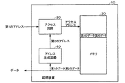
図1に、本実施形態における記憶装置の原理的な構成図を示す。記憶装置10は、メモリ20、アクセス回路30、アドレス生成回路40を含む。メモリ20は、第1のデータを記憶すると共に、該第1のデータに関連付けて第2のデータを記憶する。より具体的には、メモリ20は、第1のデータを記憶すると共に、該第1のデータの記憶領域に関連付けられた記憶領域に第2のデータを記憶する。例えば第1のデータがアクセスアドレスによって指定されるページに記憶される場合、第2のデータは該ページの冗長部に記憶される。メモリ20は、アクセスアドレスに対応して第1及び第2のデータを出力する。アクセス回路30は、外部の図示しないホストから指示された第1のアドレス、又はアドレス生成回路40によって生成された第2のアドレスのいずれかをアクセスアドレスとしてメモリ20に出力し、メモリ20に対するアクセスを実行する。アドレス生成回路40は、アクセス回路30によって出力されたアクセスアドレスに対応してメモリ20から出力されたデータの少なくとも一部に基づいて第2のアドレスを生成する。より具体的には、アドレス生成回路40は、メモリ20から出力された第2のデータに基づいて第2のアドレスを生成する。
【0032】
このような構成の記憶装置10において、第1のアクセスモード(通常アクセスモード)では、アクセス回路30は、ホストから指示された第1のアドレス(第1のデータにアクセスするための第1のアドレス)をアクセスアドレスとして出力し、メモリ20にアクセスする。第1のアドレスに対応してメモリ20から出力された第1及び第2のデータは、ホストに対して供給される。一方、第2のアクセスモード(連続アクセスモード)では、記憶装置10は、ホストから指示されたアドレスに対してアクセスを実行し、アクセスされた結果出力されたデータの一部を抽出して関連するアドレスを生成し、該アドレスを用いて再アクセスを実行することができる。
【0033】
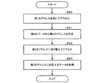
図2に、第2のアクセスモードにおける動作フローの一例を示す。まず、アクセス回路30は、ホストから指示された第1のアドレスを用いてメモリ20にアクセスする(ステップS50)。次に、アドレス生成回路40は、第1のアドレスに対応してメモリ20から出力された第1及び第2のデータのうち、第2のデータに基づいて(より具体的には、第2のデータの少なくとも一部を抽出して)、第2のアドレスを生成する(ステップS51)。このとき、第1又は第2のデータが、予め決められた条件を満足したとき(或いは満足しないとき)のみ第2のアドレスを生成することが望ましい。
【0034】
アドレス生成回路40によって第2のアドレスが生成されると、アクセス回路30は、第1のアドレスから第2のアドレスに切り替えてアクセスアドレスとして出力する(ステップS52)。すなわち、アクセス回路30は、第1のアドレスから第2のアドレスに切り替えて、第2のアドレスを用いてメモリ20を再アクセスする。そして、第2のアドレスに対応してメモリ20から出力された第1又は第2のデータをホスト側に供給する(ステップS53)。ここで、第2のアドレスに対応してメモリ20から出力された第1又は第2のデータが、上述の条件を満足しなくなるまで(或いは満足するまで)、再び該第2のデータに基づいて生成したアドレスを用いて再アクセスを行うようにしてもよい。
【0035】
このような記憶装置10によれば、ホスト側から第1のアドレスを用いた1回のアクセスを実行するのみで、メモリ20に対して複数回のアクセスが可能となる。そのため、ホストに処理負荷をかけることなく、アクセス速度の低下を抑えることができる。メモリ20は、揮発性又は不揮発性に限定されるものではないが、アクセス速度が遅いものである方がより顕著な効果を得ることができる。そのため、アクセス速度が遅い不揮発性のフラッシュメモリに適用することが望ましい。
【0036】
なお、記憶装置10において、メモリ20に対して第1のアドレスを用いた初回のアクセスで第1のデータを出力しないようにすることも可能である。また、アクセス回路30により第2のアドレスが出力される場合、該第2のアドレスは、第1のアドレスの一部のみを変更したものであってもよい。
【0037】
以下では、本実施形態における記憶装置10を、不揮発性のフラッシュメモリ装置(広義には半導体記憶装置)に適用した場合について説明する。
【0038】
図3に、フラッシュメモリ装置のハードウェア構成例を示す。フラッシュメモリ装置(半導体記憶装置)100は、メモリ110、コマンドシーケンサ120、アドレスセレクタ130、アドレス生成回路140を含む。メモリ110は、データレジスタ112を含む。アドレス生成回路140は、データ判定回路142、アドレス抽出回路144を含む。
【0039】
図1におけるメモリ20の機能は、メモリ110により実現される。図1におけるアクセス回路30の機能は、コマンドシーケンサ120及びアドレスセレクタ130により実現される。図1におけるアドレス生成回路40の機能は、アドレス生成回路140により実現される。
【0040】
メモリ110は、フラッシュEEPROMを用いて構成され、ページ単位でデータが記憶されている。各ページのデータ(ページデータ)は、データ部と冗長部とを含む。データ部には、例えば512バイト(B)分の主データ(第1のデータ)が記憶される。冗長部には、主データに対応した例えば16バイト分の関連データ(第2のデータ)が記憶される。アドレスセレクタ130から出力された内部アドレス(アクセスアドレス)iAdrに対応してメモリ110から出力されるページデータは、データレジスタ112に記憶される。アドレス生成回路140には、データレジスタ112に記憶されたページデータの少なくとも一部が供給される。また、ホストに対して、例えばデータバス幅単位でデータレジスタ112に記憶されたページデータが分割して出力される。
【0041】
コマンドシーケンサ120は、フラッシュメモリ装置100の各部の制御を司る。コマンドシーケンサ120には、外部(例えばホスト)から各種制御信号が入力される。制御信号には、チップセレクトxCS、コマンドラッチイネーブルCLE、アドレスラッチイネーブルALE、リードイネーブルxRD、ライトイネーブルxWR、ビジーxBUSYがある。チップセレクトxCSは、ホストからフラッシュメモリ装置100にアクセスするためのイネーブル信号である。コマンドラッチイネーブルCLEは、ホストから指定されるコマンドをフラッシュメモリ装置100内の内部レジスタに取り込むための信号である。アドレスラッチイネーブルALEは、ホストから指示されたアドレスをフラッシュメモリ装置100内に取り込むための信号である。リードイネーブルxRDは、メモリ110から出力されたデータをデータバス幅単位でシリアル出力させるための信号である。ライトイネーブルxWRは、ホストからの書き込みデータをフラッシュメモリ装置100内に取り込むための信号である。ビジーxBUSYは、フラッシュメモリ装置100の内部動作状態を示す信号である。
【0042】
コマンドシーケンサ120は、これら制御信号と内部動作状態により、メモリ110に対して書き込み又は読み出しのタイミング制御を行う。
【0043】
アドレスセレクタ130は、アドレスAdr(第1のアドレス)及びアドレスsAdr(第2のアドレス)のうちいずれか一方を内部アドレスiAdrとして出力する。アドレスAdrは、図示しないホストから指示されるアドレスである。アドレスsAdrは、アドレス生成回路140によって生成されるアドレス(又はその一部)である。
【0044】
アドレス生成回路140では、データ判定回路142において、データレジスタ112から供給されるページデータの少なくとも一部に基づいて、所与の条件を満たすか否かが判定される。その結果、所与の条件を満たしたときには、アドレス抽出回路144において、データレジスタ112から供給されるページデータの少なくとも一部からアドレスsAdrが抽出される。
【0045】
このようなフラッシュメモリ装置100は、ホストから指示されたアドレス(第1のアドレス)を用いてアクセスされた主データ(第1のデータ)に対応した関連データ(第2のデータ)に基づいて、再アクセス用のアドレス(第2のアドレス)を生成する。そのため、アクセスに先立って、メモリ110には、各ページの冗長部に、次のページデータのアドレスを決定するための関連データが書き込まれている。また、再アクセス用のアドレスを用いて得られたデータを用いて、再度アドレスを生成して再々アクセスを行うこともできる。
【0046】
図4に、フラッシュメモリ装置の動作タイミングの一例を示す。チップセレクトxCSにより選択状態になったフラッシュメモリ装置100では、ホストから指示されたアドレスAdr(第1のアドレス)を用いてメモリ110にアクセスが行われる。アドレスAdrによりメモリ110の第1のページデータがアクセスされたものとすると、データレジスタ112には第1のページデータが記憶される。その後、データ判定回路142では、第1のページデータの少なくとも一部に基づいて、予め決められた条件を満足したか否かが判定される。その結果、条件を満足したと判定されたとき、アドレス抽出回路144では、第1のページデータから抽出してアドレスsAdr(第2のアドレス)を生成する。アドレスセレクタ130は、アドレスAdrからアドレスsAdrに切り替えて内部アドレスiAdrとして出力する。そして、該内部アドレスiAdrを用いて再アクセスされた結果、アドレスsAdrに対応してメモリ110から出力された第2のページデータがデータレジスタ112に記憶される。データレジスタ112に記憶された第2のページデータは、例えばホスト側に供給される。
【0047】
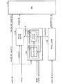
図5に、フラッシュメモリ装置の要部の詳細な構成例を示す。ここで、内部アドレスiAdr(アクセスアドレス)は、ホストから指示されるアドレスAdr(第1のアドレス)、又はアドレスAdrの中位ビットのみがデータレジスタ112から抽出されたアドレスデータに置換されたアドレス(第2のアドレス)である。そのため、アドレスセレクタ130は、アドレスAdrの中位ビットであるAdr[21:9]を、アドレス生成回路140から出力される内部アドレスレジスタデータi_AdrsReg[12:0]に切り替えることができる。
【0048】
アドレス生成回路140のデータ判定回路142は、コンパレータ143を含む。アドレス生成回路140のアドレス抽出回路144は、アドレスレジスタ145を含む。コンパレータ143は、データレジスタ112に含まれるページデータ(i_Data[15:0])の一部と、予め決められた判定条件に対応したデータとを比較する。その比較結果は、アドレスレジスタ145に入力される。アドレスレジスタ145は、コンパレータ143の比較結果に基づきデータレジスタ112に含まれるページデータの少なくとも一部(例えばi_Data[12:0])をラッチする。アドレスレジスタ145は、内部アドレスレジスタデータi_AdrsReg[12:0]をアドレスセレクタ130に出力する。
【0049】
タイミング信号i_xNextは、コマンドシーケンサ120から供給されるタイミング信号である。このタイミング信号i_xNextは、ホストからのコマンド設定により第2のアクセスモードのときアクティブとなる。タイミング信号i_xNextにより、アドレスセレクタ130の切り替え制御や、アドレス生成回路140の動作制御が行われる。
【0050】
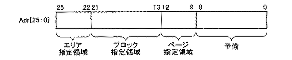
図6に、ホストから出力されるアドレスAdrについて説明するための図を示す。アドレスAdr[25:22]はエリア指定領域、アドレスAdr[21:13]はブロック指定領域、アドレスAdr[12:9]はページ指定領域である。したがって、アドレスセレクタ130によりアドレスAdr[21:9]を切り替えることにより、指定するブロック又はページを切り替えることが可能となる。
【0051】
次にフラッシュメモリ装置100の構成による効果を述べるために、まず比較例について説明する。
【0052】
図7に、比較例における半導体記憶装置の構成例を示す。比較例における半導体記憶装置(狭義にはフラッシュメモリ装置)200は、フラッシュEEPROMにより構成されるメモリ210を含む。半導体記憶装置200は、ホスト220から指定されたアドレスに対するアクセスのみを実行する。半導体記憶装置200は、該アドレスに対応してメモリ210から出力されたデータをホスト220に対して出力する。
【0053】
図8に、比較例における半導体記憶装置のタイミング図の一例を示す。ここでは、ファイルのデータのように、複数のページに分散されたデータを読み出す場合を示している。まずホスト220は、ファイル管理情報を参照して、読み出したいファイルの記憶位置のページの先頭アドレス(第1のリードアドレス)を特定する。そして、ホスト220は、半導体記憶装置200に対し、コマンドによりリードアクセスを指示する(T1)。その後、ホスト220は、半導体記憶装置200に対して3バイト(B)分の第1のリードアドレスを与える(T2)。半導体記憶装置200は、第1のリードアドレスに対応するページデータ(F_Data)を読み出してデータレジスタに記憶し、1バイトずつホスト220に対して出力する(T3)。ホスト220は、ファイル管理情報から次のページデータを読み出すべきか否かを判別し、次のアドレスを準備する(T4)。
【0054】
ホスト220は、再び半導体記憶装置200に対し、コマンドによりリードアクセスを指示する(T5)。その後、ホスト220は、半導体記憶装置200に対して3バイト(B)分の第1のリードアドレスに対応するページデータの次のページの先頭の第2のリードアドレスを与える(T6)。半導体記憶装置200は、第2のリードアドレスに対応するページデータ(S_Data)を読み出してデータレジスタに記憶し、1バイトずつホスト220に対して出力する(T7)。
【0055】
図9に、図3に示すフラッシュメモリ装置100のタイミング図の一例を示す。ここでも、図8と同様に、ファイルのデータのように複数のページに分散されたデータを読み出す場合を示している。まずホストは、ファイル管理情報を参照して、読み出したいファイルの記憶位置に対応するページの先頭アドレスを特定する。そして、ホストは、フラッシュメモリ装置100に対し、コマンドによりリードアクセスを指示する(T10)。その後、ホストは、フラッシュメモリ装置100に対して3バイト分のリードアドレスを与え、ビジーxBUSYでアドレスセレクタ130を初期化する(T11)。フラッシュメモリ装置100では、リードアドレスに対応するページデータがデータレジスタ112に記憶される。アドレス生成回路140は、読み出したデータの冗長部を用いて判定処理を行い、次のリードアドレスを保持する(T12)。アドレスセレクタ130は、保持した次のリードアドレスを出力する。これにより、メモリ110からは、次のページのページデータが出力される(T13)。
【0056】
このように、比較例における半導体記憶装置200では、図8に示すように期間T4におけるホストの判定処理後に次のアクセスが開始されるのに対し、フラッシュメモリ装置100では、図9に示すように期間T12で判定処理を内部で行い、直ちに次のアクセスを連続して行うことができる。すなわち、フラッシュメモリ装置100では、ホストからの1回のアクセス要求により、その出力データをホスト側に出力することなく、かつ装置内部で判別して繰り返しアクセスすることができる。その結果、アクセス速度の低下を抑えることができる。
【0057】
次に、このようなフラッシュメモリ装置100の使用法について具体的に説明する。
(第1の例)
第1の例では、フラッシュメモリ装置100は、正常データの追跡読み出しを実行することができる。フラッシュメモリ装置100のメモリ110では、ページ単位に正常又は不良であるかが管理される。したがって、不良ページから読み出されたデータは、信頼性にかける。そこで、不良ページの場合に代替先となるアドレスを用意しておく。そして、アクセスされたページが不良と判定されたときに、代替先のアドレスにアクセスすることで、正常データのみを連続して読み出すことができる。そのため、メモリ110では、ページデータの冗長部に1ビットの良否判定ビットと代替先アドレスが保持される。こうすることで、不良ページから読み出されたデータの使用と不良ページへのアクセスを回避し、信頼性を向上させることができる。更に冗長部の良否判定ビット等のフラグ情報を複数個記録しておくことで、フラグ情報の信頼性を向上させることができ、更に装置全体の信頼性を向上させることができる。
【0058】
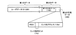
図10に、フラッシュメモリ装置100で正常データの追跡読み出しを行うためのページ構成例を示す。ページデータは、528バイトである。ページデータは、データ部と冗長部とを含む。冗長部のデータは、データ部の記憶領域に関連付けられた記憶領域に記憶される。データ部には、512バイトのユーザデータ(第1のデータ)が記憶される。冗長部には、計16バイトの第1及び第2の冗長データが記憶される。そのうち、2バイトの第2の冗長データは、1ビット(b)の良否判定ビットと、13ビットの代替先アドレスとを含む。良否判定ビットが「1」のとき当該ページが正常ページであることを示し、良否判定ビットが「0」のとき当該ページが不良ページであることを示す。代替先アドレスは、当該ページが不良ページであるときに再アクセスを行うためのアドレスである。
【0059】
図11に、正常データの追跡読み出しを行うアクセスフローの一例を示す。まず、フラッシュメモリ装置100では、ホストから指示されたアドレスを用いてメモリ110にアクセスされる(ステップS300)。すなわち、アドレスセレクタ130は、ホストから指示されたアドレス(第1のアドレス)をメモリ110に出力する。メモリ110では、ホストから指示されたアドレスのページに記憶された第1及び第2のデータが出力され、第1及び第2のデータはデータレジスタ112に保持される。次にデータ判定回路142のコンパレータ143において、冗長部の良否判定ビットが「1」であるか否かが判定される(ステップS301)。
【0060】
コンパレータ143において良否判定ビットが「0」と判定されたとき(ステップS302:N)、すなわち当該ページが正常ページではないと判定されたとき、冗長部の代替先アドレスがアドレスレジスタ145にラッチされる(ステップS303)。アドレスレジスタ145にラッチされた代替先アドレスは、内部アドレスレジスタデータi_AdrsReg[12:0]としてアドレスセレクタ130に対して出力される。アドレスセレクタ130は、アドレスAdr[21:9]を内部アドレスレジスタデータi_AdrsReg[12:0]に置換したアクセスアドレス(第2のアドレス)によりメモリ110にアクセスする(ステップS304)。
【0061】
そしてステップS301に戻り、メモリ110から第2のアドレスに対応して出力されたページデータが正常ページであるか否かが、再び判定される。
【0062】
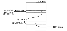
一方、ステップS302で、コンパレータ143において良否判定ビットが「1」と判定されたとき(ステップS302:Y)、すなわち当該ページが正常ページであると判定されたとき、データレジスタ112に記憶されたページデータをホストに対して1バイトずつ出力し(ステップS305)、一連のアクセスが終了する(エンド)。
【0063】
図12に、正常データの追跡読み出しの動作を模式的に示す。初回アクセスでは、ホストからの指示アドレス(第1のアドレス)を用いてメモリ110がアクセスされる。その結果、第1のアドレスに対応するページデータが不良ページである場合、当該ページの冗長部に設定される代替先アドレスを用いて第2のアドレスが生成される。その後、第2のアドレスを用いてメモリ110に再アクセスが行われる。そして、再アクセスした第2のアドレスに対応するページデータが再び不良ページである場合、当該ページの冗長部に設定される代替先アドレスを用いて再び再々アクセス用のアドレス(広義には第2のアドレス)が生成され、メモリ110に対し再々アクセスが行われる。そして、再々アクセスが行われたページが正常ページであるときには、ページデータのユーザデータ(第1のデータ)が出力される。
【0064】
このように、読み出したページデータが不良ページのデータであった場合に、代替先アドレスのページにアクセスされる。そして、このようにアクセスされるページが正常ページとなるまで代替先アドレスのページデータが繰り返し読み出される。
【0065】
これにより、ホストによるメモリへのアクセスと判定の繰り返し処理を省略することができると共に、ページ単位に正常ページ又は不良ページを管理するアドレス変換テーブルの作成が不要となる。したがって、ホストからフラッシュメモリ装置100に対しては、単純なアクセスのみで処理することができ、処理負荷の軽減し、アクセス速度の低下を抑えることができる。
(第2の例)
第2の例では、フラッシュメモリ装置100は、関連する副データへのアクセスを実行することができる。フラッシュメモリ装置100のメモリ110では、ページ単位に副データの有無が管理される。これにより、ホストで処理されるアプリケーションで主データと副データとを関連付ける必要がなく、より下位層でデータ間の関連付けを行うことができるので、ホスト側の処理負荷を軽減することができる。
【0066】
図13に、フラッシュメモリ装置100で、関連する副データへのアクセスを行うためのページ構成例を示す。ページデータのデータ部には、512バイトのユーザデータ(第1のデータ)が記憶される。冗長部には、計16バイトの第1及び第2の冗長データが記憶される。そのうち、2バイトの第2の冗長データは、1ビットのデータ種別指示ビットと、13ビットの副データの先頭アドレスとを含む。データ種別指示ビットが「1」のとき副データがあることを示し、データ種別指示ビットが「0」のとき副データがないことを示す。副データの先頭アドレスは、データ種別指示ビットにより副データがあると指定されたときに再アクセスを行うためのアドレスである。なお、主データとしては例えば画像ファイル、副データとしては例えば音声ファイルがある。
【0067】
図14に、副データへのアクセスフローの一例を示す。ここでは、ホストからのコマンドによって、副データにアクセスするモードに設定されているものとする。まず、フラッシュメモリ装置100では、ホストから指示されたアドレスを用いてメモリ110にアクセスされる(ステップS310)。すなわち、アドレスセレクタ130は、ホストから指示されたアドレス(第1のアドレス)をメモリ110に出力する。メモリ110では、ホストから指示されたアドレスのページの第1及び第2のデータが出力され、第1及び第2のデータはデータレジスタ112に保持される。次にデータ判定回路142のコンパレータ143において、冗長部のデータ種別指示ビットが「1」であるか否かが判定される(ステップS311)。
【0068】
コンパレータ143においてデータ種別指示ビットが「1」と判定されたとき(ステップS312:N)、すなわち副データがあると判定されたとき、冗長部の副データの先頭アドレスがアドレスレジスタ145にラッチされる(ステップS313)。アドレスレジスタ145にラッチされた副データの先頭アドレスは、内部アドレスレジスタデータi_AdrsReg[12:0]としてアドレスセレクタ130に対して出力される。アドレスセレクタ130は、アドレスAdr[21:9]を内部アドレスレジスタデータi_AdrsReg[12:0]に置換したアクセスアドレス(第2のアドレス)によりメモリ110にアクセスする(ステップS314)。
【0069】
そして、メモリ110から第2のアドレスに対応して出力されたページのユーザデータを副データ(例えば音声ファイル)としてデータレジスタ112に記憶して副データを出力する(ステップS315)。その後、一連のアクセスが終了する(エンド)。
【0070】
一方、ステップS312で、コンパレータ143においてデータ種別判定ビットが「0」と判定されたとき(ステップS312:N)、すなわち副データがないと判定されたとき、一連のアクセスが終了する(エンド)。
【0071】
図15に、副データへのアクセス動作を模式的に示す。初回アクセスでは、ホストからの指示アドレス(第1のアドレス)を用いてメモリ110がアクセスされる。その結果、第1のアドレスに対応するページの冗長部を参照して副データがあると判定された場合、当該ページの冗長部に設定される副データの先頭アドレスを用いて第2のアドレスが生成される。その後、第2のアドレスを用いて再アクセスが行われる。そして、再アクセスした第2のアドレスに対応するページデータのデータ部が副データとして出力される。
【0072】
なお、ホストからのコマンドによって通常アクセスモードに設定されている場合には、初回アクセスによって副データへのアクセスを実行しない。
【0073】
このように、ページデータの冗長部において副データの有無を指示し、冗長部に設定された副データのアドレスにより再アクセスが可能になるように構成した。これにより、主データの最初のアドレスから副データにアクセスすることができるようになる。したがって、ホスト側で処理されるアプリケーションで主データと副データとを関連付けて処理する必要がなくなる。すなわち、より下位層で関連付けを行うことができ、ホスト側の処理負荷を軽減することができる。
(第3の例)
第3の例では、フラッシュメモリ装置100は、ファイルに対応した連続アクセスを実行することができる。そのため、フラッシュメモリ装置100のメモリ110では、ページ単位にリンク先の有無が管理される。これにより、分散されて記憶されたファイルのデータを、ホストから例えば1ページ単位に指示されることなく読み出すことができ、処理負荷を軽減することができる。
【0074】
図16に、フラッシュメモリ装置100で、ファイルに対応した連続アクセスを行うためのページ構成例を示す。ページデータのデータ部には、512バイトのユーザデータ(第1のデータ)が記憶される。冗長部には、計16バイトの第1及び第2の冗長データが記憶される。そのうち、2バイトの第2の冗長データは、1ビットのリンク指示ビットと、13ビットのリンク先アドレスとを含む。リンク指示ビットが「1」のときリンク先があることを示し、リンク指示ビットが「0」のときリンク先がないことを示す。リンク先アドレスは、リンク指示ビットによりリンク先があると指定されたときに再アクセスを行うためのアドレスである。
【0075】
図17に、連続アクセスのアクセスフローの一例を示す。まず、フラッシュメモリ装置100では、ホストから指示されたアドレスを用いてメモリ110にアクセスされる(ステップS320)。すなわち、アドレスセレクタ130は、ホストから指示されたアドレス(第1のアドレス)をメモリ110に出力する。メモリ110では、ホストから指示されたアドレスのページの第1及び第2のデータが出力され、第1及び第2のデータがデータレジスタ112に保持される。データレジスタ112に保持されたデータは、1バイト単位で順次ホスト側に出力される(ステップS321)。次にデータ判定回路142のコンパレータ143において、冗長部のリンク指示ビットが「1」であるか否かが判定される(ステップS322)。
【0076】
コンパレータ143においてリンク指示ビットが「1」と判定されたとき(ステップS323:Y)、すなわちリンク先があると判定されたとき、冗長部のリンク先アドレスがアドレスレジスタ145にラッチされる(ステップS324)。アドレスレジスタ145にラッチされたリンク先アドレスは、内部アドレスレジスタデータi_AdrsReg[12:0]としてアドレスセレクタ130に対して出力される。アドレスセレクタ130は、アドレスAdr[21:9]を内部アドレスレジスタデータi_AdrsReg[12:0]に置換したアクセスアドレス(第2のアドレス)によりメモリ110にアクセスする(ステップS325)。
【0077】
そして、再びメモリ110から第2のアドレスに対応して出力されたページのユーザデータをデータレジスタ112に記憶し、ホスト側に順次出力するため、ステップS321に戻る。
【0078】
一方、ステップS323で、コンパレータ143においてリンク指示ビットが「0」と判定されたとき(ステップS323:N)、すなわちリンク先がないと判定されたとき、一連のアクセスが終了する(エンド)。
【0079】
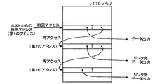
図18に、連続アクセス動作を模式的に示す。初回アクセスでは、ホストからの指示アドレス(第1のアドレス)を用いてメモリ110がアクセスされる。そして、まずメモリ110から第1のアドレスに対応して出力されたページデータのデータ部がホストに対し出力される。続いて、第1のアドレスに対応するページの冗長部を参照してリンク先があると判定された場合、当該ページの冗長部に設定されるリンク先アドレスを用いて第2のアドレスが生成される。その後、第2のアドレスを用いて再アクセスが行われる。そして、再アクセスした第2のアドレスに対応するページデータのデータ部が出力される。
【0080】
このように、最初のページにアクセスした後は、フラッシュメモリ装置100のページデータの冗長部に含まれる次のリンク先アドレスを保持し、データ出力後に該リンク先アドレスを用いて連続アクセスを行う。こうすることで、ファイルエンドとなるまでアクセスを繰り返すことができ、ホストから1ページ単位でコマンドを用いた指示を受ける必要がなくなる。その結果、ホストから指示する必要がなくなり、ホスト上のメモリ等の資源を有効活用でき、かつホストの処理負荷を軽減することができるようになる。
(第4の例)
上述の第1〜第3の例に示したようなページデータの冗長部の各種ビットを2以上組み合わせて構成することも可能である。データ種別指示ビット及びリンク指示ビットのうち少なくとも一方を、良否判定ビットと組み合わせて構成する場合、良否判定ビットの判定結果を最も優先度を高くしてアクセスすることが望ましい。
【0081】
図19に、フラッシュメモリ装置100におけるページ構成の他の例を示す。ページデータのデータ部には、512バイトのユーザデータ(第1のデータ)が記憶される。冗長部には、計16バイトの第1及び第2の冗長データが記憶される。そのうち、2バイトの第2の冗長データは、1ビットの良否判定ビットと、1ビットのデータ種別指示ビットと、1ビットのリンク指示ビットと、13ビットのアドレスとを含む。良否判定ビット、データ種別ビット及びリンク指示ビットについては、上述したものと同様であるため説明を省略する。13ビットのアドレスは、良否判定ビット、データ種別ビット及びリンク指示ビットのいずれかの判定結果に応じて、代替先アドレス、副データの先頭アドレス又はリンク先アドレスとなる。
【0082】
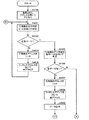
図20及び図21に、冗長部に良否判定ビット、データ種別ビット及びリンク指示ビットが組み合わされた場合のフラッシュメモリ装置のアクセスフローの一例を示す。まず、フラッシュメモリ装置100では、ホストから指示されたアドレスを用いてメモリ110にアクセスされる(ステップS400)。すなわち、アドレスセレクタ130は、ホストから指示されたアドレス(第1のアドレス)をメモリ110に出力する。メモリ110では、ホストから指示されたアドレスのページの第1及び第2のデータが出力され、第1及び第2のデータがデータレジスタ112に保持される。次にデータ判定回路142のコンパレータ143において、冗長部の良否判定ビットが「1」であるか否かが判定される(ステップS401)。
【0083】
コンパレータ143において良否判定ビットが「0」と判定されたとき(ステップS402:N)、すなわち当該ページが正常ページではないと判定されたとき、冗長部の代替先アドレスがアドレスレジスタ145にラッチされる(ステップS403)。アドレスレジスタ145にラッチされた代替先アドレスは、内部アドレスレジスタデータi_AdrsReg[12:0]としてアドレスセレクタ130に対して出力される。アドレスセレクタ130は、アドレスAdr[21:9]を内部アドレスレジスタデータi_AdrsReg[12:0]に置換したアクセスアドレス(第2のアドレス)によりメモリ110にアクセスする(ステップS404)。
【0084】
そしてステップS401に戻り、メモリ110から第2のアドレスに対応して出力されたページデータが正常ページであるか否かが、再び判定される。
【0085】
一方、ステップS402で、コンパレータ143において良否判定ビットが「1」と判定されたとき(ステップS402:Y)、すなわち当該ページが正常ページであると判定されたとき、データ判定回路142のコンパレータ143において、冗長部のデータ種別指示ビットが「1」であるか否かが判定される(ステップS405)。
【0086】
コンパレータ143においてデータ種別指示ビットが「1」と判定されたとき(ステップS406:Y)、すなわち副データがあると判定されたとき、冗長部の副データの先頭アドレスがアドレスレジスタ145にラッチされる(ステップS407)。アドレスレジスタ145にラッチされた副データの先頭アドレスは、内部アドレスレジスタデータi_AdrsReg[12:0]としてアドレスセレクタ130に対して出力される。アドレスセレクタ130は、アドレスAdr[21:9]を内部アドレスレジスタデータi_AdrsReg[12:0]に置換したアクセスアドレス(第2のアドレス)によりメモリ110にアクセスする(ステップS408)。
【0087】
そして、メモリ110から第2のアドレスに対応して出力されたページのユーザデータを、副データ(例えば音声ファイル)としてデータレジスタ112に記憶し、副データを出力する(ステップS409)。その後、一連のアクセス処理を終了することができる(エンド)が、ここではステップS409でデータ出力後、リンク先の有無を判別する処理を行う(図21のステップS411)。
【0088】
一方、ステップS406で、コンパレータ143においてデータ種別指示ビットが「0」と判定されたとき(ステップS406:N)、すなわち副データがないと判定されたとき、図21のステップS410でデータ出力後、リンク先の有無を判別する処理を行う。
【0089】
ステップS410では、アクセスされたページデータのデータ部及び冗長部がデータレジスタ112に記憶される。データレジスタ112では、1バイト単位でホストにデータ部のユーザデータが出力される。次にデータ判定回路142のコンパレータ143において、冗長部のリンク指示ビットが「1」であるか否かが判定される(ステップS411)。
【0090】
コンパレータ143においてリンク指示ビットが「1」と判定されたとき(ステップS412:Y)、すなわちリンク先があると判定されたとき、冗長部のリンク先アドレスがアドレスレジスタ145にラッチされる(ステップS413)。アドレスレジスタ145にラッチされたリンク先アドレスは、内部アドレスレジスタデータi_AdrsReg[12:0]としてアドレスセレクタ130に対して出力される。アドレスセレクタ130は、アドレスAdr[21:9]を内部アドレスレジスタデータi_AdrsReg[12:0]に置換したアクセスアドレス(第2のアドレス)によりメモリ110にアクセスする(ステップS414)。そして、再びメモリ110から第2のアドレスに対応して出力されたページのユーザデータをデータレジスタ112に記憶すると共に、図20のステップS401に戻る。
【0091】
一方、図21のステップS412で、コンパレータ143においてリンク指示ビットが「0」と判定されたとき(ステップS412:N)、すなわちリンク先がないと判定されたとき、一連のアクセスが終了する(エンド)。
【0092】
以上説明した実施形態では、半導体記憶装置として、不揮発性で、かつアクセス速度が遅いフラッシュメモリを含むものを例に説明したが、これに限定されるものではない。例えば、揮発性のメモリであるSRAMやDRAMを含む半導体記憶装置であってもよい。
【0093】
なお、第1〜第4の例では、いずれも特定のコマンドに応じた動作フロー説明したもので、本発明がこれら動作フローに限定されるものではない。
【0094】
なおまた、本発明は上述した実施の形態に限定されるものではなく、本発明の要旨の範囲内で種々の変形実施が可能である。
【0095】
また、本発明のうち従属請求項に係る発明においては、従属先の請求項の構成要件の一部を省略する構成とすることもできる。また、本発明の1の独立請求項に係る発明の要部を、他の独立請求項に従属させることもできる。
【図面の簡単な説明】
【図1】本実施形態における記憶装置の原理的な構成のブロック図。
【図2】連続アクセスモードにおける動作フローの一例を示すフロー図。
【図3】フラッシュメモリ装置のハードウェア構成例を示すブロック図。
【図4】フラッシュメモリ装置の動作例を示すタイミング図。
【図5】フラッシュメモリ装置の要部の詳細な構成例を示すブロック図。
【図6】ホストから出力されるアドレスの説明図。
【図7】比較例における半導体記憶装置の構成例を示すブロック図。
【図8】比較例における半導体記憶装置の動作例を示すタイミング図。
【図9】フラッシュメモリ装置の動作例を示すタイミング図。
【図10】正常データの追跡読み出しのためのページ構成例を示す説明図。
【図11】正常データの追跡読み出しのアクセス例を示すフロー図。
【図12】正常データの追跡読み出しの動作例を示す模式図。
【図13】副データへのアクセスのためのページ構成例を示す説明図。
【図14】副データへのアクセス例を示すフロー図。
【図15】副データへのアクセス動作例を示す模式図。
【図16】連続アクセスを行うためのページ構成例を示す説明図。
【図17】連続アクセスのアクセス例を示すフロー図。
【図18】連続アクセス動作例を示す模式図。
【図19】冗長部に良否判定ビット、データ種別ビット及びリンク指示ビットが組み合わされた場合のページ構成例を示す説明図。
【図20】冗長部に良否判定ビット、データ種別ビット及びリンク指示ビットが組み合わされた場合のアクセス例の前半部を示すフロー図。
【図21】冗長部に良否判定ビット、データ種別ビット及びリンク指示ビットが組み合わされた場合のアクセス例の後半部を示すフロー図。
【符号の説明】
10 記憶装置、20、110、210 メモリ、30 アクセス回路、40 アドレス生成回路、100 フラッシュメモリ装置(半導体記憶装置)、112データレジスタ、120 コマンドシーケンサ、130 アドレスセレクタ、140 アドレス生成回路、142 データ判定回路、143 コンパレータ、144 アドレス抽出回路、145 アドレスレジスタ、200 半導体記憶装置、220 ホスト[0001]
TECHNICAL FIELD OF THE INVENTION
The present invention relates to a storage device and a control method thereof.
[0002]
[Prior art]
As one of semiconductor storage devices (storage device in a broad sense), there is a flash memory device having a built-in flash memory such as a flash EEPROM (Electrically Erasable Programmable Read-Only Memory). This flash memory device is nonvolatile and rewritable, although the number of times of rewriting is limited. Therefore, with an increase in the capacity of a built-in memory, a flash memory device is often used as a file memory for storing file management information. For example, a flash memory device is used as an external storage device of a personal computer, a PDA (Personal Digital Assistant) or a digital camera instead of a conventional hard disk device as a memory card.
[0003]
When accessing data of a file stored in a flash memory device, an operating system (OS) executed on a host (CPU) that controls a personal computer, a PDA, or the like refers to the file management information and refers to the file management information. The access using the address corresponding to the storage position is instructed. The flash memory device outputs data stored corresponding to the address specified by the host.
[0004]
Since such file management information is frequently updated, local concentration of rewriting may occur in a predetermined area in the flash memory. Therefore, address conversion between a logical address managed by the OS and a physical address of the flash memory is controlled (for example, refer to Patent Document 1). This makes it possible to average the number of rewrites in units of memory blocks, thereby extending the life of the flash memory device.
[0005]
[Patent Document 1]
JP 2000-285001 A
[0006]
[Problems to be solved by the invention]
However, in other storage devices such as the flash memory device described above, a logical address specified by a host is converted into a physical address, and only access to the physical address is executed. Therefore, even when a plurality of data accessed and read are associated with each other, the host determines whether or not there is an association between the plurality of data and then accesses the data again as necessary. Had gone. Therefore, there is a problem that a processing load is applied to the host, and the access speed is reduced. In particular, when the reading speed is low as in a flash memory, there is a problem that the processing capability of the entire system including the host is significantly reduced.
[0007]
The present invention has been made in view of the above technical problems, and an object of the present invention is to provide a storage device capable of executing a series of accesses without imposing a processing load on a host, and a control thereof. It is to provide a method.
[0008]
[Means for Solving the Problems]
In order to solve the above problem, the present invention provides a memory for storing first data and for storing second data in a storage area associated with a storage area for the first data; An access circuit for accessing a storage area of the memory corresponding to either the first address or the second address for accessing the memory; and reading from the memory corresponding to the first address by the access circuit. An address generating circuit for generating the second address based on the output second data.
[0009]
In the storage device according to the present invention, the storage area for the first data and the storage area for the second data may exist in the same page of the memory.
[0010]
Further, in the storage device according to the present invention, the access circuit can switch from the first address to the second address to access a storage area of the memory corresponding to the second address.
[0011]
In the present invention, when accessed based on the first address, the second address is generated by the second data stored in the memory in association with the first data. Then, the access circuit can access the memory by using either the first or second address. Therefore, the memory can be accessed from the outside by using the second address in the storage device only by accessing the storage device based on the first address. In particular, by using the data read as a result of the access using the second address to generate a re-access address (in a broad sense, the second address), the access to the memory in the device can be prevented. Can be repeated. Therefore, even if a plurality of data are associated, there is no need to externally perform an association determination process. As a result, the external processing load can be reduced, and as a result, the processing capacity of the system can be improved.
[0012]
In the storage device according to the present invention, the memory holds the first and second data in page units, and the second data includes a pass / fail judgment bit indicating whether the page is defective or normal. An alternative destination address, wherein the second address is generated based on the alternative destination address on condition that the page is defective by a pass / fail determination bit included in the second data. Is also good.
[0013]
According to the present invention, it is possible to omit the repetitive processing of accessing and determining a memory outside the apparatus, and it is not necessary to create an address conversion table for managing a normal page or a defective page in page units. Therefore, externally, the storage device can be processed with only simple access, so that the processing load can be reduced and the access speed can be prevented from lowering.
[0014]
Further, in the storage device according to the present invention, the access circuit may repeatedly access the storage area of the memory using an alternative destination address of the accessed page until the pass / fail determination bit indicates that the page is normal. Can be.
[0015]
According to the present invention, the reliability of data can be further improved, and the access speed can be improved.
[0016]
Further, in the storage device according to the present invention, the second data includes a data type indication bit indicating presence / absence of sub-data and a sub-data address, and the second address is a data included in the second data. It may be generated based on the sub data address on condition that the type indication bit has sub data.
[0017]
In the present invention, the presence or absence of sub-data is indicated by the second data associated with the first data, and re-access is enabled by the set address of the sub-data. This makes it possible to access the sub data from the first address of the main data. Therefore, there is no need for an externally processed application to associate and process the main data and the sub data. That is, the association can be performed at a lower layer, and the external processing load can be reduced.
[0018]
In the storage device according to the present invention, the second data includes a link instruction bit indicating the presence or absence of a link destination and a link destination address, and the second address includes a link instruction bit included in the second data. It may be generated based on a link destination address included in the second data, provided that the bit indicates that the bit has a link destination.
[0019]
In the present invention, after the first access, the next link destination address included in the second data is held, and after data output, continuous access can be performed using the link destination address. By doing so, access can be repeated until the end of the file is reached, and it is not necessary to receive an instruction using a command in a predetermined unit from the outside.
[0020]
In the storage device according to the present invention, the memory may be a data rewritable nonvolatile memory.
[0021]
Here, the memory may be an electrically or optically erasable data in a given unit.
[0022]
According to the present invention, the second data stored in association with the first data may be set at the time of manufacture or initialization, and even if the power is frequently cut off, the access speed may be reduced. It is possible to provide a storage device capable of suppressing the decrease in the number.
[0023]
In the storage device according to the present invention, the memory may be a flash memory.
[0024]
According to the present invention, it is possible to provide a relatively large-capacity and inexpensive storage device that prevents a reduction in the processing speed of the entire system even when the power supply is frequently cut off. Also, even when the power is cut off, since the related information is retained in the redundant unit, it is highly possible that the storage contents such as the file management information will be safe without being destroyed, thereby improving reliability. Can be. For example, according to the present invention, even if the power is cut off when rewriting the file management information or the like over a plurality of pages, the link and the like are maintained, and the reliability is improved without losing the file management information and the like. Can be.
[0025]
The present invention relates to a control method of a storage device having a memory for storing first data and storing a second data in association with the first data, the method comprising: accessing the first data. Reading second data associated with the first data from the memory based on the first address, generating a second address based on the second data, and corresponding to the second address; The present invention relates to a method of controlling a storage device accessing a storage area of the memory.
[0026]
The present invention is also a control method of a storage device having a memory for storing first data in page units and storing second data in association with the first data, wherein the first data is stored in the first data. The second data including a pass / fail determination bit indicating whether the page is normal or defective and an alternative destination address is read based on the first address for accessing the page, and it is determined by the pass / fail determination bit that the page is defective. When shown, the present invention relates to a method of controlling a storage device that generates a second address based on the alternative destination address and accesses a storage area of the memory corresponding to the second address.
[0027]
The present invention is also a method for controlling a storage device having a memory for storing first data and storing second data in association with the first data, the method comprising: accessing the first data. The second data including the data type determination bit and the sub-data address is read based on the first address, and when the data type determination bit indicates that the sub-data is included, the second data is read based on the sub-data address. And a method of controlling a storage device that accesses a storage area of the memory corresponding to the second address.
[0028]
The present invention is also a method for controlling a storage device having a memory for storing first data and storing second data in association with the first data, the method comprising: accessing the first data. Reading the second data including a link indication bit indicating the presence or absence of a link destination and a link destination address based on the first address of the link destination address. When the link destination indication bit indicates that the link destination exists, the link destination address is read. And generating a second address based on the second address, and controlling a storage device that accesses a storage area of the memory corresponding to the second address.
[0029]
Further, in the storage device control method according to the present invention, the storage area for the first data and the storage area for the second data may exist in the same page of the memory.
[0030]
BEST MODE FOR CARRYING OUT THE INVENTION
Hereinafter, preferred embodiments of the present invention will be described in detail with reference to the drawings. The embodiments described below do not unduly limit the contents of the invention described in the claims. In addition, all of the configurations described below are not necessarily essential components of the invention.
[0031]
FIG. 1 shows a principle configuration diagram of a storage device according to the present embodiment. The
[0032]
In the
[0033]
FIG. 2 shows an example of an operation flow in the second access mode. First, the
[0034]
When the second address is generated by the
[0035]
According to the
[0036]
In the
[0037]
Hereinafter, a case will be described in which the
[0038]
FIG. 3 shows an example of a hardware configuration of the flash memory device. The flash memory device (semiconductor storage device) 100 includes a
[0039]
The function of the
[0040]
The
[0041]
The
[0042]
The
[0043]
The
[0044]
In the
[0045]
Such a
[0046]
FIG. 4 shows an example of the operation timing of the flash memory device. In the
[0047]
FIG. 5 shows a detailed configuration example of a main part of the flash memory device. Here, the internal address iAdr (access address) is an address Adr (first address) specified by the host, or an address in which only middle bits of the address Adr are replaced with address data extracted from the data register 112 ( Second address). Therefore, the
[0048]
The
[0049]
The timing signal i_xNext is a timing signal supplied from the
[0050]
FIG. 6 is a diagram for explaining the address Adr output from the host. Address Adr [25:22] is an area designation area, address Adr [21:13] is a block designation area, and address Adr [12: 9] is a page designation area. Therefore, by switching the address Adr [21: 9] by the
[0051]
Next, a comparative example will be described first to describe effects of the configuration of the
[0052]
FIG. 7 shows a configuration example of a semiconductor memory device in a comparative example. A semiconductor memory device (flash memory device in a narrow sense) 200 in the comparative example includes a
[0053]
FIG. 8 shows an example of a timing chart of the semiconductor memory device in the comparative example. Here, a case is shown in which data distributed over a plurality of pages, such as file data, is read. First, the
[0054]
The
[0055]
FIG. 9 shows an example of a timing chart of the
[0056]
As described above, in the
[0057]
Next, a method of using the
(First example)
In the first example, the
[0058]
FIG. 10 shows an example of a page configuration for performing normal data tracking reading in the
[0059]
FIG. 11 shows an example of an access flow for performing tracking reading of normal data. First, in the
[0060]
When the pass / fail determination bit is determined to be “0” by the comparator 143 (step S302: N), that is, when it is determined that the page is not a normal page, the replacement destination address of the redundant part is latched in the address register 145. (Step S303). The replacement destination address latched by the address register 145 is output to the
[0061]
Then, returning to step S301, it is determined again whether or not the page data output from the
[0062]
On the other hand, when the pass / fail judgment bit is determined to be “1” by the
[0063]
FIG. 12 schematically shows the operation of tracking reading of normal data. In the first access, the
[0064]
As described above, when the read page data is the data of the defective page, the page of the replacement destination address is accessed. Then, the page data of the replacement destination address is repeatedly read until the page accessed in this way becomes a normal page.
[0065]
As a result, it is possible to omit the process of repeatedly accessing and determining the memory by the host, and it is not necessary to create an address translation table for managing a normal page or a defective page in page units. Therefore, the host can process the
(Second example)
In the second example, the
[0066]
FIG. 13 shows an example of a page configuration for accessing related sub-data in the
[0067]
FIG. 14 shows an example of an access flow to the sub data. Here, it is assumed that a mode for accessing the sub data has been set by a command from the host. First, in the
[0068]
When the
[0069]
Then, the user data of the page output from the
[0070]
On the other hand, when the data type determination bit is determined to be “0” by the
[0071]
FIG. 15 schematically shows an operation of accessing the sub data. In the first access, the
[0072]
When the normal access mode is set by a command from the host, the access to the sub-data is not executed by the first access.
[0073]
As described above, the presence or absence of the sub data is indicated in the redundant part of the page data, and the re-access is enabled by the address of the sub data set in the redundant part. This makes it possible to access the sub data from the first address of the main data. Therefore, it is not necessary for the application processed on the host side to process the main data and the sub data in association with each other. That is, the association can be performed at a lower layer, and the processing load on the host side can be reduced.
(Third example)
In the third example, the
[0074]
FIG. 16 shows a page configuration example for performing continuous access corresponding to a file in the
[0075]
FIG. 17 shows an example of an access flow of continuous access. First, in the
[0076]
When the link instruction bit is determined to be "1" by the comparator 143 (step S323: Y), that is, when it is determined that there is a link destination, the link destination address of the redundant part is latched in the address register 145 (step S324). ). The link destination address latched by the address register 145 is output to the
[0077]
Then, the user data of the page output from the
[0078]
On the other hand, when the link instruction bit is determined to be “0” by the
[0079]
FIG. 18 schematically shows the continuous access operation. In the first access, the
[0080]
As described above, after the first page is accessed, the next link destination address included in the redundant part of the page data of the
(Fourth example)
It is also possible to configure by combining two or more various bits of the redundant portion of the page data as shown in the above-described first to third examples. When at least one of the data type indication bit and the link indication bit is configured in combination with the pass / fail judgment bit, it is desirable to access the result of the pass / fail judgment bit with the highest priority.
[0081]
FIG. 19 shows another example of a page configuration in the
[0082]
20 and 21 show an example of an access flow of the flash memory device when the pass / fail judgment bit, the data type bit, and the link instruction bit are combined in the redundant portion. First, in the
[0083]
When the pass / fail determination bit is determined to be “0” by the comparator 143 (step S402: N), that is, when it is determined that the page is not a normal page, the replacement destination address of the redundant part is latched in the address register 145. (Step S403). The replacement destination address latched by the address register 145 is output to the
[0084]
Then, returning to step S401, it is determined again whether or not the page data output from the
[0085]
On the other hand, when the pass / fail judgment bit is determined to be “1” by the
[0086]
When the data type indication bit is determined to be “1” by the comparator 143 (step S 406: Y), that is, when it is determined that there is sub data, the head address of the sub data of the redundant part is latched in the address register 145. (Step S407). The head address of the sub data latched in the address register 145 is output to the
[0087]
Then, the user data of the page output from the
[0088]
On the other hand, when the data type indication bit is determined to be “0” by the
[0089]
In step S410, the data part and the redundant part of the accessed page data are stored in the data register 112. The data register 112 outputs the user data of the data portion to the host in byte units. Next, the
[0090]
When the link instruction bit is determined to be "1" by the comparator 143 (step S412: Y), that is, when it is determined that there is a link destination, the link destination address of the redundant part is latched in the address register 145 (step S413). ). The link destination address latched by the address register 145 is output to the
[0091]
On the other hand, when the link instruction bit is determined to be “0” in the
[0092]
In the above-described embodiments, the semiconductor memory device includes a flash memory that is nonvolatile and has a low access speed. However, the present invention is not limited to this. For example, a semiconductor storage device including a volatile memory such as an SRAM or a DRAM may be used.
[0093]
In the first to fourth examples, the operation flow according to a specific command has been described, and the present invention is not limited to these operation flows.
[0094]
Further, the present invention is not limited to the above-described embodiment, and various modifications can be made within the scope of the present invention.
[0095]
Further, in the invention according to the dependent claims of the present invention, a configuration in which some of the constituent elements of the dependent claims are omitted may be adopted. In addition, a main part of the invention according to one independent claim of the present invention can be made dependent on another independent claim.
[Brief description of the drawings]
FIG. 1 is a block diagram showing a basic configuration of a storage device according to an embodiment.
FIG. 2 is a flowchart showing an example of an operation flow in a continuous access mode.
FIG. 3 is a block diagram illustrating an example of a hardware configuration of a flash memory device.
FIG. 4 is a timing chart showing an operation example of the flash memory device.
FIG. 5 is a block diagram showing a detailed configuration example of a main part of the flash memory device.
FIG. 6 is an explanatory diagram of an address output from a host.
FIG. 7 is a block diagram illustrating a configuration example of a semiconductor memory device in a comparative example.
FIG. 8 is a timing chart showing an operation example of a semiconductor memory device in a comparative example.
FIG. 9 is a timing chart showing an operation example of the flash memory device.
FIG. 10 is an explanatory diagram showing an example of a page configuration for tracking reading of normal data.
FIG. 11 is a flowchart showing an example of access for tracking reading of normal data.
FIG. 12 is a schematic diagram showing an operation example of tracking reading of normal data.
FIG. 13 is an explanatory diagram showing an example of a page configuration for accessing sub data.
FIG. 14 is a flowchart showing an example of accessing sub data.
FIG. 15 is a schematic diagram showing an operation example of accessing sub data.
FIG. 16 is an explanatory diagram showing an example of a page configuration for performing continuous access.
FIG. 17 is a flowchart showing an example of continuous access.
FIG. 18 is a schematic diagram showing an example of a continuous access operation.
FIG. 19 is an explanatory diagram showing an example of a page configuration when a pass / fail judgment bit, a data type bit, and a link instruction bit are combined with a redundant part.
FIG. 20 is a flowchart showing the first half of an access example when a pass / fail judgment bit, a data type bit, and a link instruction bit are combined with a redundant part.
FIG. 21 is a flowchart showing the latter half of an access example when a pass / fail judgment bit, a data type bit, and a link instruction bit are combined with a redundant part.
[Explanation of symbols]
Claims (14)
前記第1のデータにアクセスするための第1のアドレス、又は第2のアドレスのいずれかに対応する前記メモリの記憶領域にアクセスするアクセス回路と、
前記アクセス回路により前記第1のアドレスに対応して前記メモリから読み出された第2のデータに基づいて、前記第2のアドレスを生成するアドレス生成回路とを含むことを特徴とする記憶装置。A memory that stores the first data and stores the second data in a storage area associated with the storage area of the first data;
An access circuit for accessing a storage area of the memory corresponding to either a first address for accessing the first data or a second address;
A storage device, comprising: an address generation circuit configured to generate the second address based on second data read from the memory corresponding to the first address by the access circuit.
前記第1のデータの記憶領域と前記第2のデータの記憶領域とは、前記メモリの同一ページに存在することを特徴とする記憶装置。In claim 1,
The storage device according to claim 1, wherein the storage area for the first data and the storage area for the second data exist in the same page of the memory.
前記アクセス回路は、
前記第1のアドレスから前記第2のアドレスに切り替えて、前記第2のアドレスに対応する前記メモリの記憶領域にアクセスすることを特徴とする記憶装置。In claim 1 or 2,
The access circuit,
A storage device, switching from the first address to the second address and accessing a storage area of the memory corresponding to the second address.
前記メモリは、
ページ単位で前記第1及び第2のデータを保持し、
前記第2のデータは、
当該ページが不良又は正常のいずれかを示す良否判定ビットと代替先アドレスとを含み、
前記第2のアドレスは、
前記第2のデータに含まれる良否判定ビットにより当該ページが不良であることを示すことを条件に、前記代替先アドレスに基づいて生成されることを特徴とする記憶装置。In any one of claims 1 to 3,
The memory is
Holding the first and second data in page units,
The second data is
The page includes a pass / fail judgment bit indicating whether the page is defective or normal and an alternative destination address,
The second address is
A storage device, which is generated based on the replacement destination address, on condition that the page is defective by a pass / fail judgment bit included in the second data.
前記アクセス回路は、
前記良否判定ビットにより当該ページが正常であることを示すまで、アクセスするページの代替先アドレスを用いて繰り返し前記メモリの記憶領域にアクセスすることを特徴とする記憶装置。In claim 4,
The access circuit,
A storage device, wherein the storage area of the memory is repeatedly accessed using an alternate destination address of a page to be accessed until the page is determined to be normal by the pass / fail judgment bit.
前記第2のデータは、
副データの有無を示すデータ種別指示ビットと副データアドレスとを含み、
前記第2のアドレスは、
前記第2のデータに含まれるデータ種別指示ビットが副データを有することを示すことを条件に、前記副データアドレスに基づいて生成されることを特徴とする記憶装置。In any one of claims 1 to 5,
The second data is
A data type indicating bit indicating the presence or absence of sub data and a sub data address,
The second address is
A storage device, which is generated based on the sub data address, provided that a data type indication bit included in the second data indicates that the data type has sub data.
前記第2のデータは、
リンク先の有無を示すリンク指示ビットとリンク先アドレスとを含み、
前記第2のアドレスは、
前記第2のデータに含まれるリンク指示ビットがリンク先を有することを示すことを条件に、前記第2のデータに含まれるリンク先アドレスに基づいて生成されることを特徴とする記憶装置。In any one of claims 1 to 6,
The second data is
A link indication bit indicating the presence or absence of a link destination and a link destination address,
The second address is
A storage device, which is generated based on a link destination address included in the second data, on condition that the link instruction bit included in the second data indicates that the link destination has a link destination.
前記メモリは、
データの書き換え可能な不揮発性メモリであることを特徴とする記憶装置。In any one of claims 1 to 7,
The memory is
A storage device, which is a data rewritable nonvolatile memory.
前記メモリは、
フラッシュメモリであることを特徴とする記憶装置。In claim 8,
The memory is
A storage device, which is a flash memory.
前記第1のデータにアクセスするための第1のアドレスに基づき、前記第1のデータに関連付けられた第2のデータを前記メモリから読み出し、
前記第2のデータに基づいて第2のアドレスを生成し、
前記第2のアドレスに対応する前記メモリの記憶領域にアクセスすることを特徴とする記憶装置の制御方法。A method for controlling a storage device having a memory for storing first data and storing a second data in association with the first data,
Reading, from the memory, second data associated with the first data based on a first address for accessing the first data;
Generating a second address based on the second data;
A method of controlling a storage device, comprising accessing a storage area of the memory corresponding to the second address.
前記第1のデータにアクセスするための第1のアドレスに基づき、当該ページの正常又は不良を示す良否判定ビットと代替先アドレスとを含む第2のデータを読み出し、
前記良否判定ビットにより当該ページが不良であることを示すとき、前記代替先アドレスに基づいて第2のアドレスを生成し、
前記第2のアドレスに対応する前記メモリの記憶領域にアクセスすることを特徴とする記憶装置の制御方法。A method of controlling a storage device having a memory for storing first data in page units and storing second data in association with the first data,
Based on a first address for accessing the first data, read second data including a pass / fail determination bit indicating whether the page is normal or defective and an alternative destination address,
Generating a second address based on the replacement destination address when the page is defective by the pass / fail determination bit;
A method of controlling a storage device, comprising accessing a storage area of the memory corresponding to the second address.
前記第1のデータにアクセスするための第1のアドレスに基づき、データ種別判定ビットと副データアドレスとを含む第2のデータを読み出し、
前記データ種別判定ビットが副データを有することを示すとき、前記副データアドレスに基づいて第2のアドレスを生成し、
前記第2のアドレスに対応する前記メモリの記憶領域にアクセスすることを特徴とする記憶装置の制御方法。A method for controlling a storage device having a memory for storing first data and storing a second data in association with the first data,
Reading second data including a data type determination bit and a sub data address based on a first address for accessing the first data;
Generating a second address based on the sub data address when the data type determination bit indicates having sub data;
A method of controlling a storage device, comprising accessing a storage area of the memory corresponding to the second address.
前記第1のデータにアクセスするための第1のアドレスに基づき、リンク先の有無を示すリンク指示ビットとリンク先アドレスとを含む第2のデータを読み出し、
前記リンク先指示ビットがリンク先を有することを示すとき、前記リンク先アドレスに基づいて前記第2のアドレスを生成し、
前記第2のアドレスに対応する前記メモリの記憶領域にアクセスすることを特徴とする記憶装置の制御方法。A method for controlling a storage device having a memory for storing first data and storing a second data in association with the first data,
Based on a first address for accessing the first data, reading second data including a link instruction bit indicating the presence or absence of a link destination and a link destination address;
Generating the second address based on the link destination address when the link destination indication bit indicates that the link destination is provided;
A method of controlling a storage device, comprising accessing a storage area of the memory corresponding to the second address.
前記第1のデータの記憶領域と前記第2のデータの記憶領域とは、前記メモリの同一ページに存在することを特徴とする制御方法。In any one of claims 10 to 13,
The control method according to claim 1, wherein the storage area for the first data and the storage area for the second data exist in the same page of the memory.
Priority Applications (1)
| Application Number | Priority Date | Filing Date | Title |
|---|---|---|---|
| JP2002307091A JP2004145446A (en) | 2002-10-22 | 2002-10-22 | Storage device and its control method |
Applications Claiming Priority (1)
| Application Number | Priority Date | Filing Date | Title |
|---|---|---|---|
| JP2002307091A JP2004145446A (en) | 2002-10-22 | 2002-10-22 | Storage device and its control method |
Publications (1)
| Publication Number | Publication Date |
|---|---|
| JP2004145446A true JP2004145446A (en) | 2004-05-20 |
Family
ID=32453649
Family Applications (1)
| Application Number | Title | Priority Date | Filing Date |
|---|---|---|---|
| JP2002307091A Withdrawn JP2004145446A (en) | 2002-10-22 | 2002-10-22 | Storage device and its control method |
Country Status (1)
| Country | Link |
|---|---|
| JP (1) | JP2004145446A (en) |
Cited By (3)
| Publication number | Priority date | Publication date | Assignee | Title |
|---|---|---|---|---|
| JP2013200802A (en) * | 2012-03-26 | 2013-10-03 | Mega Chips Corp | Semiconductor memory |
| JP2015103093A (en) * | 2013-11-26 | 2015-06-04 | ウィンボンド エレクトロニクス コーポレーション | Flash memory, bad block management method, and management program |
| WO2016056290A1 (en) * | 2014-10-09 | 2016-04-14 | ソニー株式会社 | Memory controller, memory system, storage device, information processing system, and storage control method |
-
2002
- 2002-10-22 JP JP2002307091A patent/JP2004145446A/en not_active Withdrawn
Cited By (3)
| Publication number | Priority date | Publication date | Assignee | Title |
|---|---|---|---|---|
| JP2013200802A (en) * | 2012-03-26 | 2013-10-03 | Mega Chips Corp | Semiconductor memory |
| JP2015103093A (en) * | 2013-11-26 | 2015-06-04 | ウィンボンド エレクトロニクス コーポレーション | Flash memory, bad block management method, and management program |
| WO2016056290A1 (en) * | 2014-10-09 | 2016-04-14 | ソニー株式会社 | Memory controller, memory system, storage device, information processing system, and storage control method |
Similar Documents
| Publication | Publication Date | Title |
|---|---|---|
| US8145829B2 (en) | Flash memory device capable of preventing read disturbance | |
| JP5053552B2 (en) | Data storage device having heterogeneous non-volatile memory and driving method thereof | |
| KR100533682B1 (en) | Data managing device and method for flash memory | |
| JP2013097416A (en) | Storage device and computer | |
| JPH1185609A (en) | Semiconductor memory and data managing method therefor | |
| JP3875139B2 (en) | Nonvolatile semiconductor memory device, data write control method thereof, and program | |
| US4975872A (en) | Dual port memory device with tag bit marking | |
| JP2008243265A (en) | Information recorder and method of controlling thereof | |
| JP2004145446A (en) | Storage device and its control method | |
| JP2007233838A (en) | Control method for memory system | |
| US20020083291A1 (en) | Nonvolatile semiconductor memory | |
| EP1804166B1 (en) | Memory device and information processing apparatus | |
| JP2867965B2 (en) | Data processing device and data processing method | |
| JP2008033379A (en) | Nonvolatile storage apparatus | |
| KR20100114305A (en) | Data storage device and data storage system including of the same | |
| JP2002358233A (en) | Memory controller, flash memory system having memory controller and control method for flash memory | |
| US6029210A (en) | Memory initialization system selectively outputting a data between a normal data stored in the memory and a fixed value according to a registered access state | |
| JP2004192426A (en) | Storage device and its control method | |
| JP2009271828A (en) | Storage device, storage device control system, method for controlling storage device, and program | |
| JP2003122630A (en) | Memory controller, flash memory system having memory controller, and method for controlling flash memory | |
| JP2008129851A (en) | Processing unit | |
| CN117130556A (en) | Micro file system in optical module and operation method | |
| JP2003196087A (en) | Memory addressing system of microcontroller and page mapping device | |
| JP2003296105A (en) | Data processor | |
| JP2001209578A (en) | Management system for memory update history |
Legal Events
| Date | Code | Title | Description |
|---|---|---|---|
| A300 | Withdrawal of application because of no request for examination |
Free format text: JAPANESE INTERMEDIATE CODE: A300 Effective date: 20060110 |