JP2004140178A - Chemical mechanical polishing apparatus - Google Patents
Chemical mechanical polishing apparatus Download PDFInfo
- Publication number
- JP2004140178A JP2004140178A JP2002303346A JP2002303346A JP2004140178A JP 2004140178 A JP2004140178 A JP 2004140178A JP 2002303346 A JP2002303346 A JP 2002303346A JP 2002303346 A JP2002303346 A JP 2002303346A JP 2004140178 A JP2004140178 A JP 2004140178A
- Authority
- JP
- Japan
- Prior art keywords
- polishing
- wafer
- polishing pad
- grooves
- chemical mechanical
- Prior art date
- Legal status (The legal status is an assumption and is not a legal conclusion. Google has not performed a legal analysis and makes no representation as to the accuracy of the status listed.)
- Pending
Links
Images


Abstract
Description
【0001】
【発明の属する技術分野】
本発明は、化学的機械研磨技術、特に、パターニングされた半導体ウエハ(以下、パターン付きウエハという。)のパターニングされた側の主面を化学的機械研磨(Chmical Mechical Polishing)する技術に関する。
【0002】
【従来の技術】
最近、パターン付きウエハの表面を機械的な作用と化学的な作用との組み合わせによって研磨する化学的機械研磨装置が使用されて来ている。従来のこの種の化学的機械研磨装置は、回転されるベースプレートの上に貼着された研磨パッドと、ワークであるウエハを保持するウエハ保持ヘッドとを備えており、ウエハ保持ヘッドによって保持したウエハをスラリと称される研磨溶液が滴下される研磨パッドに擦り付けて化学的機械研磨するように構成されている。
【0003】
この研磨パッドとしては、ポリウレタンを含浸させた不織布の上に発泡ポリウレタンが積層されて構成されており、発泡ポリウレタン側がウエハを研磨する側となっている。従来のこの種の研磨パッドとしては、例えば、次のものがある。第一は、口径が1.5mmの複数個の孔を発泡ポリウレタンの表面に5mmの間隔をもって全面にわたって開設することにより、スラリを複数個の孔によって保持してウエハの表面に接触させるように構成した研磨パッドである。第二は、幅が2mmで深さが0.5〜0.8mmの溝を発泡ポリウレタンの表面に15mmの間隔をもって格子状に形成することにより、スラリを格子状の溝によって保持してウエハの表面に接触させるように構成した研磨パッドである。第三は、発泡ポリウレタンの表面に口径が約1.5mmの孔を5mm間隔をもって全面にわたって開設するとともに、幅が孔の口径よりも小さく深さが約0.3mmの複数条の溝を孔の間隔よりも大きい間隔をもって格子状に形成することにより、ウエハの研磨パッドへの吸着を防止しつつスラリの必要量を抑え、かつ、研磨パッドの経時劣化を低減させるように構成した研磨パッドである。なお、このような研磨パッドを述べてある文献としては、特開平11−235656号公報、がある。
【0004】
【発明が解決しようとする課題】
しかしながら、孔だけが開設された第一の研磨パッドにおいては、研磨が終了した後にウエハ保持ヘッドを上昇させてウエハを取り除こうとした時に、ウエハが研磨パッドに吸着してしまうという問題点がある。また、溝だけが形成された第二の研磨パッドにおいては、深い溝が高密度に形成されていることにより下層の軟質層であるポリウレタンを含浸させた不織布への局所的な圧力負荷が発生するために、均一性が劣化し易くなるという問題点がある。さらに、孔と格子状の溝とを有する第三の研磨パッドにおいては、スラリが研磨時の研磨パッドの回転による遠心力によって格子状の溝に落ちて格子状の溝を通って研磨パッドの外へ排出されてしまうために、研磨速度が低下してしまうという問題点がある。そして、従来のこの種の化学的機械研磨装置においては、パターン付きウエハの被研磨面にスクラッチ(研磨傷)が発生するのを防止することが最も重要である。
【0005】
本発明の目的は、スクラッチの発生やワークの吸着および研磨速度の低下を防止しつつ、被研磨面を高い精度をもって均一に研磨することができる化学的機械研磨装置を提供することにある。
【0006】
本発明の前記ならびにその他の目的と新規な特徴は、本明細書の記述および添付図面から明らかになるであろう。
【0007】
【課題を解決するための手段】
本願において開示される発明のうち代表的なものの概要を説明すれば、次の通りである。
【0008】
すなわち、研磨面に複数条の溝と複数個の孔とを有する研磨パッドを備えた化学的機械研磨装置であって、前記複数条の溝は同心円の環状溝に形成され、かつ、これら環状溝の隣り合うもの同士の間隔が前記孔の隣り合うもの同士の間隔以下に設定されていることを特徴とする。
【0009】
前記した手段によれば、研磨パッドの回転による遠心力に関わらず、スラリを環状溝によって保持することができるために、研磨速度の低下を防止することができる。また、環状溝は被研磨面と研磨面との間を外部に接続することができるために、被研磨面が研磨面に真空吸着する現象が発生するのを防止することができる。さらに、スクラッチの発生原因となる異物を孔によってトラップすることができるために、スクラッチの発生を防止することができる。
【0010】
【発明の実施の形態】
以下、本発明の一実施の形態を図面に即して説明する。
【0011】
図1に示されているように、本実施の形態に係る化学的機械研磨装置10は研磨ヘッド11を備えている。研磨ヘッド11はワークであるパターン付きウエハ(以下、ウエハという。)1の直径よりも充分に大きい半径を有する円盤形状に形成されたベースプレート12を備えており、ベースプレート12は水平面内において回転自在に支持されている。ベースプレート12の下面の中心には垂直方向に配された回転軸13が固定されており、ベースプレート12は回転軸13によって回転駆動されるように構成されている。ベースプレート12の上面には図2に示された研磨パッド30が全体にわたって均一に貼着されている。研磨ヘッド11の中心線上には研磨溶液であるスラリ15を滴下するスラリ供給ノズル14が垂直方向下向きに設置されている。スラリ15は用途により多くの種類がある。例えば、酸化膜を研磨する場合には、シリカ(SiO2 )粒子を10〜20%程度含み、KOHまたはNH4 OH等によりpH10〜11程度に調整されたものが使用される。
【0012】
研磨ヘッド11の上方にはウエハ保持ヘッド16が水平に設置されている。ウエハ保持ヘッド16は研磨ヘッド11が設備されたステーションとウエハ1が一枚ずつ払い出されるローディングステーション(図示せず)との間を移送装置(図示せず)によって往復移動されるようになっており、ウエハ保持ヘッド16は研磨作業に際して極僅かに下降されるようになっている。研磨ヘッド11はウエハ1の直径よりも若干大きい直径を有する円盤形状に形成されたヘッド本体17を備えており、ヘッド本体17の下面には円形で一定深さの保持穴18が同心円に配されて没設されている。保持穴18の大きさはウエハ1の大きさよりも若干大きめに形成されている。保持穴18の中心には通気孔19が開設されており、通気孔19がエアポンプおよび真空ポンプ(いずれも図示せず)に接続されることにより、保持穴18には正圧および負圧が供給されるようになっている。ちなみに、エアポンプおよび真空ポンプは切換弁によって適宜に切り換えられるようになっている。保持穴18の下面には保持穴18の内径と略等しい外径を有する円盤形状のバッキングパッド20が、同心に配されて接着材層(図示せず)によって接着されている。バッキングパッド20はポリウレタンの発泡体によって形成されており、発泡体の多孔質かつ多孔群によってウエハ1と接する面に柔軟性の高い層が全体にわたって均一に構成されている。ヘッド本体17の下面における外周辺部には円形リング形状のリテーナリング21が当接されており、リテーナリング21は複数本のボルト(図示せず)によりヘッド本体17に締結されている。リテーナリング21は外径がヘッド本体17の外径と等しく内径が保持穴18の内径と略等しい円形リング形状に形成されている。リテーナリング21はウエハ1をその被研磨面を下端から下方に露出させた状態で、研磨作業中にウエハ1が外側に飛び出すのを阻止しつつ保持するようになっている。ヘッド本体17の中心線上には回転軸22が垂直方向上向きに突設されており、回転軸22は回転駆動装置(図示せず)によって回転駆動されるようになっている。
【0013】
研磨ヘッド11の上方のウエハ保持ヘッド16と反対側には、研磨によってダメージを受けた研磨パッド30の表層部を除去して再生させるドレッサ23が水平に設置されており、ドレッサ23は研磨パッド30に接触した状態で研磨ヘッド11に対して水平移動し得るように構成されている。ドレッサ23は研磨ヘッド11の半径よりも充分に小さい直径を有する円盤形状に形成されたベースプレート24を備えており、ベースプレート24は水平面内において回転自在に支持されている。ベースプレート24の上面の中心には垂直方向に配された回転軸25が固定されており、ベースプレート24は回転軸25によって回転駆動されるように構成されている。ベースプレート24の下面には研磨パッド30の表層部を研磨するダイヤモンドパッド26が全体にわたって均一に貼着されている。
【0014】
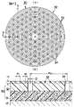
図2に示されているように、研磨パッド30はポリウレタンを含浸させた不織布31の上に発泡ポリウレタン32が積層されて構成されている。不織布(以下、軟質層部という。)31は発泡ポリウレタン32に比べて軟質に構成されており、研磨パッド30がウエハ1の形状に倣うことができるようになっている。発泡ポリウレタン(以下、硬質層部という。)32はウエハ1の表面を平坦に研磨するために硬質に構成されているが、ウエハ1から受ける荷重によってミクロンオーダーで変形することができるようになっている。研磨パッド30の研磨面である硬質層部32の表面には一定幅で一定深さの環状溝33が複数条、同心円に没設されているとともに、円柱形状の孔34が複数個一定間隔をもって格子状に配列されて開設されており、隣り合う環状溝33、33同士の間隔(ピッチ)P1 は、隣り合う孔34、34同士の間隔(ピッチ)P2 以下に設定されている。
【0015】
隣り合う環状溝33、33同士の間隔P1 は1.5〜5mmに設定することが望ましい。本実施の形態においては、隣り合う環状溝33、33同士の間隔P1 は、約1.5mmに設定されている。環状溝33の幅Wは0.25〜2mmに設定することが望ましい。本実施の形態においては、環状溝33の幅Wは約0.25mmに設定されている。環状溝33の深さHは0.15〜1.8mmに設定することが望ましい。本実施の形態においては、環状溝33の深さHは約0.4mmに設定されている。孔34の口径Dは1〜4mmに設定することが望ましい。本実施の形態においては、孔34の口径Dは約1.5mmに設定されており、隣り合う孔34、34の間隔P2 は約5.5mmに設定されている。
【0016】
次に、前記構成に係る化学的機械研磨装置の作用および効果を説明する。
【0017】
図1に示されているように、ウエハ1は被研磨面側を下向きに配された状態でウエハ保持ヘッド16のリテーナリング21内に挿入される。ウエハ1がリテーナリング21内に挿入されると、負圧が通気孔19に供給される。負圧はバッキングパッド20の多孔を通じてウエハ1の被研磨面と反対側の主面(以下、裏側面という。)に印加されるため、ウエハ1はウエハ保持ヘッド16に真空吸着される。ウエハ1を真空吸着したウエハ保持ヘッド16は移送装置によって研磨ヘッド11の真上に移送された後に下降される。ウエハ保持ヘッド16の下降によってウエハ1の被研磨面が研磨パッド30の研磨面である表面に当接すると、切換弁が切り換えられてエアが通気孔19に供給される。
【0018】
続いて、スラリ15が研磨パッド30の表面にスラリ供給ノズル14から供給されながら、研磨ヘッド11およびウエハ保持ヘッド16が回転される。ウエハ保持ヘッド16が回転されると、研磨パッド30の表面に供給されたスラリ15は同心円に没設された複数条の環状溝33群に取り込まれて保持される。この際、幅Wが約0.25mmで深さHが約0.4mmの多数条の環状溝33が約1.5mmの間隔をもって同心円に没設されているため、大量のスラリ15が研磨パッド30の研磨面である表面に保持された状態になる。
【0019】
以降、ウエハ保持ヘッド16は極僅かずつ下降される。ウエハ保持ヘッド16の下降により、ウエハ1はバッキングパッド20を介して垂直方向に付勢される。同時に、通気孔19に供給されたエアが裏側面に供給されているため、ウエハ1はエアの圧力による作用力によっても垂直方向に付勢される。したがって、ウエハ1の被研磨面は研磨パッド30の研磨面に機械的な力とエアの圧力による作用力とによって同時に付勢された状態で、研磨パッド30の研磨面に擦られる。このとき、スラリ15が環状溝33群によって保持されているために、機械的な研磨(ポリシング)に加えてそのポリシング効果を高めるメカノケミカルポリシング(mechanochemical polishing)が実施される。
【0020】
ウエハ1が研磨パッド30に機械的な力とエアの圧力による作用力とによって同時に付勢された状態で、被研磨面は研磨パッド30の多数条の環状溝33に保持された大量のスラリ15によって化学的機械研磨されるため、被研磨面の研磨パッド30による研磨量は全体にわたって均一になる。化学的機械研磨中に、ウエハ保持ヘッド16の機械的な押し力によって押されるウエハ1側から作用する不規則で複雑な歪力は、研磨ヘッド11の軟質層部31の変形および硬質層部32のミクロンオーダーの変形によって自己整合的に補正されるため、被研磨面の研磨量は全面にわたって均一になる。
【0021】
設定した研磨量の化学的機械研磨が終了した状態で、ウエハ1の被研磨面はきわめて高精度に平坦化され、かつ、絶縁膜が予め設定された層厚をもって残された状態になる。この状態のウエハ1はウエハ保持ヘッド16によって吸着保持されて研磨ヘッド11の上から移送される。この際、図1(b)に示されているように、ウエハ1に接触した環状溝33群はウエハ1の下面の外側で両端が開口した状態になっていることにより、ウエハ1が研磨パッド30の表面に吸着してしまうことはないため、ウエハ1は研磨パッド30の表面からウエハ保持ヘッド16によって確実に引き上げることができる。
【0022】
ところで、以上の化学的機械研磨においては、スラリ15に含まれる砥粒同士の凝集物、研磨中にウエハ1が破砕することによって生ずる破片や切り屑、ドレッサ23の研磨による切り屑等の異物が研磨パッド30の表面に多数存在し、これら異物はスラリ15のかけ流しでは完全に除去することができないために、研磨パッド30の表面に残留することが起きる。そして、ウエハ1の被研磨面が研磨パッド30の表面に残留した異物によって損傷されることにより、ウエハ1の被研磨面にはスクラッチが形成されてしまう。
【0023】
しかし、本実施の形態においては、研磨パッド30の硬質層部32には口径が約1.5mmの円柱形状の孔34が約5.5mmの間隔をもって全体的に開設されていることにより、研磨パッド30の表面に発生した異物を孔34群によって直ちにトラップすることができるために、ウエハ1の被研磨面が研磨パッド30の表面に残留した異物によって損傷されることによってウエハ1の被研磨面に形成されてしまうスクラッチの発生は未然に防止することができる。
【0024】
図3はスクラッチの低減効果を示すグラフである。図3において、横軸には研磨パッドの使用時間(hr)がとられており、縦軸にはスクラッチの個数がとられている。実線の折れ線Aが本実施の形態の場合を示しており、破線の折れ線Bが比較例の場合を示している。比較例は、幅が0.25mmで深さが約0.3mmの溝が発泡ポリウレタンの表面に1.5mmの間隔をもって同心円に形成されている研磨パッドを使用した場合、である。図3によれば、比較例の場合には1.5時間使用後からスクラッチの個数が指数関数的に増加し始めているのに対して、本実施の形態の場合にはスクラッチの個数の増加が見られないことが、理解される。
【0025】
図4は研磨パッドの使用時間(横軸)による研磨速度(縦軸)の推移を示すグラフである。図4において、実線の直線Cが本実施の形態の場合を示しており、破線の直線Dが比較例の場合を示している。比較例は図3の場合と同一の研磨パッドを使用した場合である。図4によれば、本実施の形態の研磨速度は比較例のそれよりも一割程度も大きいことが理解される。
【0026】
図5は別の比較例についての研磨パッドの使用時間(横軸)による研磨速度(縦軸)の推移を示すグラフであり、実線の直線Eが本実施の形態の場合を示しており、破線の直線Fが比較例の場合を示している。この比較例は発泡ポリウレタンの表面に口径が約1.5mmの孔が5mm間隔をもって全面にわたって開設されているとともに、幅が孔の口径よりも小さく深さが約0.3mmの複数条の溝が孔の間隔よりも大きい間隔をもって格子状に形成されている研磨パッドを使用した場合である。図5によれば、本実施の形態の研磨速度は比較例のそれよりも五割程度も大きいことが理解される。本実施の形態の研磨速度が比較例のそれよりも大きい理由は、次の通りであると考察される。比較例の研磨パッドにおいては、スラリが研磨時の研磨パッドの回転による遠心力によって格子状の溝に落ちて格子状の溝を通って研磨パッドの外へ排出されてしまうために、研磨速度が低下してしまう。これに対して、本実施の形態に係る研磨パッド30においては、スラリ15を保持する溝が環状溝33に形成されていることにより、スラリが研磨時の研磨パッドの回転による遠心力によって環状溝33群から外に排出されることなく保持されるために、研磨速度が低下してしまうことはない。
【0027】
図6は研磨パッドの使用時間(横軸)による研磨量の均一性(縦軸)の推移を示すグラフである。研磨量の均一性は次式によって表される特性である。
研磨量の均一性=(最大研磨量−最小研磨量)/(最大研磨量+最小研磨量)
図6において、実線の直線Gが本実施の形態の場合を示しており、破線の曲線Hが比較例の場合を示している。比較例は図3の場合と同一の研磨パッドを使用した場合である。図6で明らかな通り、比較例の場合には研磨の均一性が使用時間の経過に伴って曲線的に増加して行くのに対して、本実施の形態の場合には研磨の均一性が使用時間の経過に伴って直線的に漸増して行く。したがって、本実施の形態の場合には、研磨パッド30の寿命を長く設定することができる。
【0028】
ところで、研磨パッド30の硬質層部32の表面に形成される環状溝33および孔34の構成について究明したところ、次の結果が得られた。
【0029】
隣り合う環状溝33、33の間隔は1.5〜5mmに設定することが望ましい。隣り合う環状溝33、33の間隔が1.5mm未満であると、環状溝33が過多になり、研磨パッド30の硬質層部32の表面とウエハ1との接触面積が不足し、また、大量のスラリ15が必要になる。隣り合う環状溝33、33の間隔が5mmを超えると、環状溝33の不足によってスラリ15が不足して研磨速度が小さくなる。
【0030】
環状溝33の幅は0.25〜2mmに設定することが望ましい。環状溝33の幅が0.25mm未満であると、環状溝33の加工が困難になる。環状溝33の幅が2mmを超えると、研磨パッド30の硬質層部32の表面とウエハ1との接触面積が不足し、研磨速度が低下する。
【0031】
環状溝33の深さは0.15〜1.8mmに設定することが望ましい。環状溝の深さが0.15mm未満であると、環状溝33がないものと均等になり、研磨速度が低下する。環状溝の深さが1.8mmを超えると、研磨パッド30の硬質層部32の厚さによる制約によって環状溝を加工することが困難になる。
【0032】
孔34の口径は1〜4mmに設定することが望ましい。孔の口径が1mm未満であると、スクラッチの発生原因となる異物をトラップすることができないために、スクラッチの個数が増加してしまう。孔の口径が4mmを超えると、研磨パッド30の硬質層部32の表面とウエハ1との接触面積が不足し、研磨速度が低下する。
【0033】
なお、孔34の口径は環状溝33の幅よりも大きい方が望ましい。また、隣り合う孔34、34の間隔は5mm程度が望ましい。
【0034】
以上本発明者によってなされた発明を実施の形態に基づき具体的に説明したが、本発明は前記実施の形態に限定されるものではなく、その要旨を逸脱しない範囲で種々変更可能であることはいうまでもない。
【0035】
例えば、孔34は碁盤の目の格子状に配列するに限らず、図7に示されているように、千鳥格子状に配列してもよい。
【0036】
ウエハ保持ヘッドは前記実施の形態のように構成するに限らず、他の構成を採用してもよい。また、ウエハ保持ヘッドを上側に、研磨ヘッドを下側に配置するに限らず、ウエハ保持ヘッドを下側に、研磨ヘッドを上側に配置してもよい。さらに、ウエハ保持ヘッド側を下降させるように構成するに限らず、研磨ヘッド側を上昇させるように構成してもよい。
【0037】
以上の説明では主として本発明者によってなされた発明をその背景となった利用分野であるパターン付きウエハのパターニング側主面の凹凸を平坦化する化学的機械研磨技術に適用した場合について説明したが、それに限定されるものではなく、ダマシン技術による銅(Cu)配線を形成するのに使用される化学的機械研磨技術等の化学的機械研磨技術全般に適用することができる。
【0038】
【発明の効果】
本願において開示される発明のうち代表的なものによって得られる効果を簡単に説明すれば、次の通りである。
【0039】
研磨パッドの研磨面に複数条の環状溝を同心円に形成し、かつ、これら環状溝の隣り合うもの同士の間隔を研磨面に開設された複数個の孔の隣り合うもの同士の間隔以下に設定することにより、研磨パッドの回転による遠心力に関わらず、スラリを環状溝によって保持することができ、かつ、スクラッチの発生原因となる異物を孔によってトラップすることができるために、スクラッチの発生やワークの吸着および研磨速度の低下を防止しつつ、被研磨面を高い精度をもって均一に研磨することができる。
【図面の簡単な説明】
【図1】本発明の一実施の形態に係る化学的機械研磨装置を示しており、(a)は一部切断正面図、(b)は平面図である。
【図2】研磨パッドを示しており、(a)は平面図、(b)は(a)のb−b線に沿う断面図である。
【図3】スクラッチの低減効果を示すグラフである。
【図4】研磨パッドの使用時間による研磨速度の推移を示すグラフである。
【図5】研磨パッドの使用時間による研磨速度の推移を示すグラフである。
【図6】研磨パッドの使用時間による研磨量の均一性の推移を示すグラフである。
【図7】本発明の第二の実施の形態に係る研磨パッドを示しており、(a)は平面図、(b)は(a)のb−b線に沿う断面図である。
【符号の説明】
1…ウエハ(半導体ウエハ)、10…化学的機械研磨装置、11…研磨ヘッド、12…ベースプレート、13…回転軸、14…スラリ供給ノズル、15…スラリ、16…ウエハ保持ヘッド、17…ヘッド本体、18…保持穴、19…通気孔、20…バッキングパッド、21…リテーナリング、22…回転軸、23…ドレッサ、24…ベースプレート、25…回転軸、26…ダイヤモンドパッド、30…研磨パッド、31…軟質層部(不織布)、32…硬質層部(発泡ポリウレタン)、33…環状溝、34…孔。[0001]
TECHNICAL FIELD OF THE INVENTION
The present invention relates to a chemical mechanical polishing technique, and more particularly, to a technique of chemically mechanical polishing a main surface on a patterned side of a patterned semiconductor wafer (hereinafter, referred to as a patterned wafer).
[0002]
[Prior art]
Recently, a chemical mechanical polishing apparatus for polishing the surface of a patterned wafer by a combination of mechanical action and chemical action has been used. A conventional chemical mechanical polishing apparatus of this type includes a polishing pad stuck on a rotated base plate, and a wafer holding head for holding a wafer as a work, and a wafer held by the wafer holding head. Is rubbed against a polishing pad on which a polishing solution called a slurry is dropped to perform chemical mechanical polishing.
[0003]
This polishing pad is formed by laminating a foamed polyurethane on a nonwoven fabric impregnated with a polyurethane, and the foamed polyurethane side is a side for polishing a wafer. Conventional polishing pads of this type include, for example, the following. First, a plurality of holes having a diameter of 1.5 mm are formed on the entire surface of the polyurethane foam at intervals of 5 mm so that the slurry is held by the plurality of holes and brought into contact with the surface of the wafer. Polishing pad. Secondly, by forming grooves having a width of 2 mm and a depth of 0.5 to 0.8 mm in a grid pattern at intervals of 15 mm on the surface of the polyurethane foam, the slurry is held by the grid-shaped grooves and the wafer is formed. This is a polishing pad configured to be brought into contact with the surface. Thirdly, holes of about 1.5 mm in diameter are opened over the entire surface at 5 mm intervals on the surface of the polyurethane foam, and a plurality of grooves having a width smaller than the diameter of the holes and a depth of about 0.3 mm are formed in the holes. A polishing pad configured to be formed in a grid shape with an interval larger than the interval, thereby preventing the wafer from being attracted to the polishing pad, suppressing the required amount of slurry, and reducing the deterioration over time of the polishing pad. . As a document describing such a polishing pad, there is JP-A-11-235656.
[0004]
[Problems to be solved by the invention]
However, in the first polishing pad in which only the holes are formed, there is a problem that the wafer is attracted to the polishing pad when the wafer holding head is lifted to remove the wafer after the polishing is completed. Further, in the second polishing pad in which only the grooves are formed, a local pressure load is applied to the nonwoven fabric impregnated with the polyurethane, which is the lower soft layer, due to the deep grooves being formed at a high density. Therefore, there is a problem that the uniformity is easily deteriorated. Further, in the third polishing pad having the holes and the lattice-shaped grooves, the slurry falls into the lattice-shaped grooves by centrifugal force due to the rotation of the polishing pad during polishing, and passes through the lattice-shaped grooves to outside the polishing pad. Therefore, there is a problem that the polishing rate is reduced due to the discharge of the polishing liquid. In this type of conventional chemical mechanical polishing apparatus, it is most important to prevent scratches (polishing scratches) from being generated on the polished surface of the patterned wafer.
[0005]
SUMMARY OF THE INVENTION An object of the present invention is to provide a chemical mechanical polishing apparatus capable of uniformly polishing a surface to be polished with high accuracy while preventing generation of scratches, adsorption of a work, and reduction of a polishing rate.
[0006]
The above and other objects and novel features of the present invention will become apparent from the description of the present specification and the accompanying drawings.
[0007]
[Means for Solving the Problems]
The outline of a typical invention disclosed in the present application will be described as follows.
[0008]
That is, a chemical mechanical polishing apparatus provided with a polishing pad having a plurality of grooves and a plurality of holes on a polishing surface, wherein the plurality of grooves are formed in concentric annular grooves, and The distance between adjacent ones of the holes is set to be equal to or less than the distance between adjacent ones of the holes.
[0009]
According to the above-described means, since the slurry can be held by the annular groove regardless of the centrifugal force due to the rotation of the polishing pad, a decrease in the polishing rate can be prevented. In addition, since the annular groove can connect the surface to be polished and the surface to be polished to the outside, it is possible to prevent the phenomenon that the surface to be polished is vacuum-adsorbed to the surface to be polished. Further, since the foreign matter causing the scratch can be trapped by the hole, the generation of the scratch can be prevented.
[0010]
BEST MODE FOR CARRYING OUT THE INVENTION
Hereinafter, an embodiment of the present invention will be described with reference to the drawings.
[0011]
As shown in FIG. 1, a chemical mechanical polishing apparatus 10 according to the present embodiment includes a polishing head 11. The polishing head 11 has a disk-
[0012]
Above the polishing head 11, a
[0013]
On the opposite side of the polishing head 11 from the
[0014]
As shown in FIG. 2, the
[0015]
Distance P 1 of adjacent
[0016]
Next, the operation and effect of the chemical mechanical polishing apparatus according to the above configuration will be described.
[0017]
As shown in FIG. 1, the
[0018]
Subsequently, the polishing head 11 and the
[0019]
Thereafter, the
[0020]
In a state where the
[0021]
After the chemical mechanical polishing of the set polishing amount is completed, the surface to be polished of the
[0022]
By the way, in the above chemical mechanical polishing, foreign substances such as agglomerates of abrasive grains contained in the slurry 15, debris and chips generated by crushing the
[0023]
However, in the present embodiment, the
[0024]
FIG. 3 is a graph showing the effect of reducing scratches. In FIG. 3, the horizontal axis represents the usage time (hr) of the polishing pad, and the vertical axis represents the number of scratches. A solid broken line A indicates the case of the present embodiment, and a broken broken line B indicates the case of the comparative example. The comparative example is a case where a polishing pad is used in which grooves having a width of 0.25 mm and a depth of about 0.3 mm are formed concentrically on the surface of the polyurethane foam at intervals of 1.5 mm. According to FIG. 3, in the case of the comparative example, the number of scratches starts to increase exponentially after 1.5 hours of use, whereas in the case of the present embodiment, the number of scratches increases. It is understood that not seen.
[0025]
FIG. 4 is a graph showing the transition of the polishing rate (vertical axis) with the use time (horizontal axis) of the polishing pad. In FIG. 4, a solid line C indicates the case of the present embodiment, and a broken line D indicates the case of the comparative example. The comparative example is a case where the same polishing pad as that of FIG. 3 is used. According to FIG. 4, it is understood that the polishing rate of the present embodiment is about 10% higher than that of the comparative example.
[0026]
FIG. 5 is a graph showing a change in the polishing rate (vertical axis) with respect to the use time (horizontal axis) of the polishing pad in another comparative example. A solid line E indicates the case of the present embodiment, and a broken line. Represents the case of the comparative example. In this comparative example, a hole having a diameter of about 1.5 mm is formed over the entire surface at an interval of 5 mm on the surface of the polyurethane foam, and a plurality of grooves having a width smaller than the hole diameter and a depth of about 0.3 mm are formed. This is a case where a polishing pad formed in a lattice shape with an interval larger than the interval between the holes is used. According to FIG. 5, it is understood that the polishing rate of the present embodiment is about 50% higher than that of the comparative example. The reason why the polishing rate of the present embodiment is higher than that of the comparative example is considered as follows. In the polishing pad of the comparative example, since the slurry falls into the lattice-shaped grooves due to centrifugal force due to the rotation of the polishing pad during polishing and is discharged out of the polishing pad through the lattice-shaped grooves, the polishing speed is reduced. Will drop. On the other hand, in the
[0027]
FIG. 6 is a graph showing the transition of the uniformity of the polishing amount (vertical axis) according to the use time (horizontal axis) of the polishing pad. The uniformity of the polishing amount is a characteristic represented by the following equation.
Uniformity of polishing amount = (maximum polishing amount-minimum polishing amount) / (maximum polishing amount + minimum polishing amount)
In FIG. 6, a solid line G indicates the case of the present embodiment, and a broken line curve H indicates the case of the comparative example. The comparative example is a case where the same polishing pad as that of FIG. 3 is used. As is clear from FIG. 6, in the case of the comparative example, the polishing uniformity increases in a curve with the elapse of use time, whereas in the case of the present embodiment, the polishing uniformity is reduced. It gradually increases linearly as the use time elapses. Therefore, in the case of the present embodiment, the life of polishing
[0028]
By the way, when the configuration of the
[0029]
It is desirable that the interval between the adjacent
[0030]
It is desirable that the width of the
[0031]
It is desirable that the depth of the
[0032]
The diameter of the
[0033]
Preferably, the diameter of the
[0034]
Although the invention made by the present inventor has been specifically described based on the embodiment, the present invention is not limited to the above embodiment, and various changes can be made without departing from the gist of the invention. Needless to say.
[0035]
For example, the
[0036]
The wafer holding head is not limited to the configuration as in the above embodiment, but may adopt another configuration. Further, the wafer holding head is not limited to being arranged on the upper side and the polishing head is arranged on the lower side. The wafer holding head may be arranged on the lower side and the polishing head may be arranged on the upper side. Further, the present invention is not limited to the configuration in which the wafer holding head side is lowered, but may be configured to raise the polishing head side.
[0037]
In the above description, the case where the invention made by the present inventor is applied to a chemical mechanical polishing technique for flattening irregularities on a patterning-side main surface of a patterned wafer, which is a field of application as a background, has been described. The present invention is not limited to this, and can be applied to all chemical mechanical polishing techniques such as a chemical mechanical polishing technique used for forming copper (Cu) wiring by a damascene technique.
[0038]
【The invention's effect】
The effect obtained by the representative one of the inventions disclosed in the present application will be briefly described as follows.
[0039]
A plurality of annular grooves are formed concentrically on the polishing surface of the polishing pad, and the distance between adjacent ones of these annular grooves is set to be equal to or less than the distance between adjacent ones of a plurality of holes formed on the polishing surface. By doing so, regardless of the centrifugal force due to the rotation of the polishing pad, the slurry can be held by the annular groove, and the foreign matter that causes the scratch can be trapped by the hole. The surface to be polished can be uniformly polished with high precision while preventing the suction of the work and the reduction of the polishing rate.
[Brief description of the drawings]
FIG. 1 shows a chemical mechanical polishing apparatus according to an embodiment of the present invention, wherein (a) is a partially cut front view and (b) is a plan view.
FIGS. 2A and 2B show a polishing pad, wherein FIG. 2A is a plan view and FIG. 2B is a cross-sectional view taken along line bb of FIG.
FIG. 3 is a graph showing the effect of reducing scratches.
FIG. 4 is a graph showing a change in a polishing rate with a use time of a polishing pad.
FIG. 5 is a graph showing a change in a polishing rate according to a use time of a polishing pad.
FIG. 6 is a graph showing the transition of the uniformity of the polishing amount with the use time of the polishing pad.
7A and 7B show a polishing pad according to a second embodiment of the present invention, wherein FIG. 7A is a plan view, and FIG. 7B is a cross-sectional view taken along line bb of FIG.
[Explanation of symbols]
DESCRIPTION OF
Claims (5)
Priority Applications (1)
| Application Number | Priority Date | Filing Date | Title |
|---|---|---|---|
| JP2002303346A JP2004140178A (en) | 2002-10-17 | 2002-10-17 | Chemical mechanical polishing apparatus |
Applications Claiming Priority (1)
| Application Number | Priority Date | Filing Date | Title |
|---|---|---|---|
| JP2002303346A JP2004140178A (en) | 2002-10-17 | 2002-10-17 | Chemical mechanical polishing apparatus |
Publications (2)
| Publication Number | Publication Date |
|---|---|
| JP2004140178A true JP2004140178A (en) | 2004-05-13 |
| JP2004140178A5 JP2004140178A5 (en) | 2005-07-14 |
Family
ID=32451163
Family Applications (1)
| Application Number | Title | Priority Date | Filing Date |
|---|---|---|---|
| JP2002303346A Pending JP2004140178A (en) | 2002-10-17 | 2002-10-17 | Chemical mechanical polishing apparatus |
Country Status (1)
| Country | Link |
|---|---|
| JP (1) | JP2004140178A (en) |
Cited By (8)
| Publication number | Priority date | Publication date | Assignee | Title |
|---|---|---|---|---|
| JP2004167605A (en) * | 2002-11-15 | 2004-06-17 | Rodel Nitta Co | Polishing pad and polishing device |
| KR100568258B1 (en) | 2004-07-01 | 2006-04-07 | 삼성전자주식회사 | Polishing pad for chemical mechanical polishing and apparatus using the same |
| JPWO2007119845A1 (en) * | 2006-04-14 | 2009-08-27 | 株式会社ロキテクノ | Polishing pad for device wafer |
| US8011999B2 (en) | 2006-07-10 | 2011-09-06 | Fujitsu Semiconductor Limited | Polishing pad, method for manufacturing the polishing pad |
| US10071461B2 (en) | 2014-04-03 | 2018-09-11 | 3M Innovative Properties Company | Polishing pads and systems and methods of making and using the same |
| JP2018167371A (en) * | 2017-03-30 | 2018-11-01 | 富士紡ホールディングス株式会社 | Polishing pad |
| CN110385632A (en) * | 2019-07-19 | 2019-10-29 | 南开大学 | Magnetic-type polishing clamp and burnishing device |
| CN113524022A (en) * | 2021-09-17 | 2021-10-22 | 湖北鼎汇微电子材料有限公司 | Polishing pad and method for manufacturing semiconductor device |
-
2002
- 2002-10-17 JP JP2002303346A patent/JP2004140178A/en active Pending
Cited By (10)
| Publication number | Priority date | Publication date | Assignee | Title |
|---|---|---|---|---|
| JP2004167605A (en) * | 2002-11-15 | 2004-06-17 | Rodel Nitta Co | Polishing pad and polishing device |
| KR100568258B1 (en) | 2004-07-01 | 2006-04-07 | 삼성전자주식회사 | Polishing pad for chemical mechanical polishing and apparatus using the same |
| JPWO2007119845A1 (en) * | 2006-04-14 | 2009-08-27 | 株式会社ロキテクノ | Polishing pad for device wafer |
| US8011999B2 (en) | 2006-07-10 | 2011-09-06 | Fujitsu Semiconductor Limited | Polishing pad, method for manufacturing the polishing pad |
| US10071461B2 (en) | 2014-04-03 | 2018-09-11 | 3M Innovative Properties Company | Polishing pads and systems and methods of making and using the same |
| US10252396B2 (en) | 2014-04-03 | 2019-04-09 | 3M Innovative Properties Company | Polishing pads and systems and methods of making and using the same |
| JP2018167371A (en) * | 2017-03-30 | 2018-11-01 | 富士紡ホールディングス株式会社 | Polishing pad |
| CN110385632A (en) * | 2019-07-19 | 2019-10-29 | 南开大学 | Magnetic-type polishing clamp and burnishing device |
| CN113524022A (en) * | 2021-09-17 | 2021-10-22 | 湖北鼎汇微电子材料有限公司 | Polishing pad and method for manufacturing semiconductor device |
| CN113524022B (en) * | 2021-09-17 | 2022-01-07 | 湖北鼎汇微电子材料有限公司 | Polishing pad and method for manufacturing semiconductor device |
Similar Documents
| Publication | Publication Date | Title |
|---|---|---|
| US6193587B1 (en) | Apparatus and method for cleansing a polishing pad | |
| US8485863B2 (en) | Polishing liquids for activating and/or conditioning fixed abrasive polishing pads, and associated systems and methods | |
| KR100566787B1 (en) | Semiconductor polishing method and apparatus | |
| US6010395A (en) | Chemical-mechanical polishing apparatus | |
| EP0874390B1 (en) | Polishing method | |
| US20040009742A1 (en) | Polishing pad conditioning disks for chemical mechanical polisher | |
| JP3770752B2 (en) | Semiconductor device manufacturing method and processing apparatus | |
| JPH11156711A (en) | Polishing device | |
| JPH11868A (en) | Dressing jig for abrasive cloth surface and its manufacture | |
| US6341997B1 (en) | Method for recycling a polishing pad conditioning disk | |
| US6386963B1 (en) | Conditioning disk for conditioning a polishing pad | |
| KR20110084877A (en) | Textured platen | |
| US6302770B1 (en) | In-situ pad conditioning for CMP polisher | |
| US6394886B1 (en) | Conformal disk holder for CMP pad conditioner | |
| JPH11235656A (en) | Grinding pad | |
| JP2004140178A (en) | Chemical mechanical polishing apparatus | |
| JP2004167605A (en) | Polishing pad and polishing device | |
| US6478977B1 (en) | Polishing method and apparatus | |
| KR19980070998A (en) | Polishing apparatus, polishing member and polishing method | |
| US20070049184A1 (en) | Retaining ring structure for enhanced removal rate during fixed abrasive chemical mechanical polishing | |
| US6300248B1 (en) | On-chip pad conditioning for chemical mechanical polishing | |
| US20020187731A1 (en) | In-situ pad and wafer cleaning during chemical mechanical polishing | |
| JP2004122291A (en) | Method for polishing substrate | |
| CN110744444B (en) | Polishing pad and polishing apparatus | |
| KR100910509B1 (en) | Chemical-mechanical polishing apparatus for manufacturing semiconductor devices |
Legal Events
| Date | Code | Title | Description |
|---|---|---|---|
| A521 | Written amendment |
Free format text: JAPANESE INTERMEDIATE CODE: A523 Effective date: 20041116 |
|
| A621 | Written request for application examination |
Free format text: JAPANESE INTERMEDIATE CODE: A621 Effective date: 20041116 |
|
| A977 | Report on retrieval |
Free format text: JAPANESE INTERMEDIATE CODE: A971007 Effective date: 20070529 |
|
| A131 | Notification of reasons for refusal |
Free format text: JAPANESE INTERMEDIATE CODE: A131 Effective date: 20070605 |
|
| A02 | Decision of refusal |
Free format text: JAPANESE INTERMEDIATE CODE: A02 Effective date: 20071009 |