JP2004137480A - Fluorescent substance thin film, method for producing the same and el panel - Google Patents
Fluorescent substance thin film, method for producing the same and el panel Download PDFInfo
- Publication number
- JP2004137480A JP2004137480A JP2003326736A JP2003326736A JP2004137480A JP 2004137480 A JP2004137480 A JP 2004137480A JP 2003326736 A JP2003326736 A JP 2003326736A JP 2003326736 A JP2003326736 A JP 2003326736A JP 2004137480 A JP2004137480 A JP 2004137480A
- Authority
- JP
- Japan
- Prior art keywords
- thin film
- phosphor thin
- panel
- phosphor
- film
- Prior art date
- Legal status (The legal status is an assumption and is not a legal conclusion. Google has not performed a legal analysis and makes no representation as to the accuracy of the status listed.)
- Pending
Links
- 239000010409 thin film Substances 0.000 title claims abstract description 169
- 239000000126 substance Substances 0.000 title claims abstract description 32
- 238000004519 manufacturing process Methods 0.000 title claims abstract description 8
- 239000000463 material Substances 0.000 claims abstract description 38
- 238000000034 method Methods 0.000 claims abstract description 28
- 239000000203 mixture Substances 0.000 claims abstract description 20
- 229910052712 strontium Inorganic materials 0.000 claims abstract description 15
- 229910052749 magnesium Inorganic materials 0.000 claims abstract description 14
- 229910052684 Cerium Inorganic materials 0.000 claims abstract description 13
- 229910052693 Europium Inorganic materials 0.000 claims abstract description 13
- 229910052791 calcium Inorganic materials 0.000 claims abstract description 13
- 229910052788 barium Inorganic materials 0.000 claims abstract description 11
- 229910052727 yttrium Inorganic materials 0.000 claims abstract description 11
- 229910052725 zinc Inorganic materials 0.000 claims abstract description 11
- UCKMPCXJQFINFW-UHFFFAOYSA-N Sulphide Chemical compound [S-2] UCKMPCXJQFINFW-UHFFFAOYSA-N 0.000 claims abstract description 10
- 238000000137 annealing Methods 0.000 claims abstract description 9
- 229910052688 Gadolinium Inorganic materials 0.000 claims abstract description 7
- 229910052746 lanthanum Inorganic materials 0.000 claims abstract description 7
- 229910052691 Erbium Inorganic materials 0.000 claims abstract description 6
- 229910052689 Holmium Inorganic materials 0.000 claims abstract description 6
- 229910052765 Lutetium Inorganic materials 0.000 claims abstract description 6
- 229910052779 Neodymium Inorganic materials 0.000 claims abstract description 6
- 229910052777 Praseodymium Inorganic materials 0.000 claims abstract description 6
- 229910052772 Samarium Inorganic materials 0.000 claims abstract description 6
- 229910052771 Terbium Inorganic materials 0.000 claims abstract description 6
- 229910052775 Thulium Inorganic materials 0.000 claims abstract description 6
- 229910052769 Ytterbium Inorganic materials 0.000 claims abstract description 6
- 229910052706 scandium Inorganic materials 0.000 claims abstract description 6
- 229910052692 Dysprosium Inorganic materials 0.000 claims abstract description 5
- OAICVXFJPJFONN-UHFFFAOYSA-N Phosphorus Chemical compound [P] OAICVXFJPJFONN-UHFFFAOYSA-N 0.000 claims description 128
- 150000001875 compounds Chemical class 0.000 claims description 22
- 238000001704 evaporation Methods 0.000 claims description 18
- 230000008020 evaporation Effects 0.000 claims description 14
- 229910052796 boron Inorganic materials 0.000 claims description 4
- 239000010408 film Substances 0.000 abstract description 47
- 229910052717 sulfur Inorganic materials 0.000 abstract description 10
- 125000004430 oxygen atom Chemical group O* 0.000 abstract description 4
- 125000004434 sulfur atom Chemical group 0.000 abstract description 3
- 239000000758 substrate Substances 0.000 description 62
- 239000011575 calcium Substances 0.000 description 27
- 239000011572 manganese Substances 0.000 description 27
- 229910052984 zinc sulfide Inorganic materials 0.000 description 22
- 239000008188 pellet Substances 0.000 description 17
- 239000011777 magnesium Substances 0.000 description 13
- 239000011701 zinc Substances 0.000 description 13
- 239000007789 gas Substances 0.000 description 12
- LTPBRCUWZOMYOC-UHFFFAOYSA-N Beryllium oxide Chemical compound O=[Be] LTPBRCUWZOMYOC-UHFFFAOYSA-N 0.000 description 8
- 229910052748 manganese Inorganic materials 0.000 description 7
- 229910052710 silicon Inorganic materials 0.000 description 7
- 239000010703 silicon Substances 0.000 description 7
- 238000007740 vapor deposition Methods 0.000 description 7
- 229910018072 Al 2 O 3 Inorganic materials 0.000 description 6
- XKRFYHLGVUSROY-UHFFFAOYSA-N Argon Chemical compound [Ar] XKRFYHLGVUSROY-UHFFFAOYSA-N 0.000 description 6
- XUIMIQQOPSSXEZ-UHFFFAOYSA-N Silicon Chemical compound [Si] XUIMIQQOPSSXEZ-UHFFFAOYSA-N 0.000 description 6
- 239000011521 glass Substances 0.000 description 6
- 238000010438 heat treatment Methods 0.000 description 6
- 229910052751 metal Inorganic materials 0.000 description 6
- 239000002184 metal Substances 0.000 description 6
- 238000000103 photoluminescence spectrum Methods 0.000 description 6
- 229910052761 rare earth metal Inorganic materials 0.000 description 6
- 238000004544 sputter deposition Methods 0.000 description 6
- 238000005566 electron beam evaporation Methods 0.000 description 5
- 238000000295 emission spectrum Methods 0.000 description 5
- 239000000843 powder Substances 0.000 description 5
- 230000004044 response Effects 0.000 description 5
- VWQVUPCCIRVNHF-UHFFFAOYSA-N yttrium atom Chemical compound [Y] VWQVUPCCIRVNHF-UHFFFAOYSA-N 0.000 description 5
- 229910052581 Si3N4 Inorganic materials 0.000 description 4
- NINIDFKCEFEMDL-UHFFFAOYSA-N Sulfur Chemical compound [S] NINIDFKCEFEMDL-UHFFFAOYSA-N 0.000 description 4
- PNEYBMLMFCGWSK-UHFFFAOYSA-N aluminium oxide Inorganic materials [O-2].[O-2].[O-2].[Al+3].[Al+3] PNEYBMLMFCGWSK-UHFFFAOYSA-N 0.000 description 4
- 229910052786 argon Inorganic materials 0.000 description 4
- BJXXCWDIBHXWOH-UHFFFAOYSA-N barium(2+);oxygen(2-);tantalum(5+) Chemical compound [O-2].[O-2].[O-2].[O-2].[O-2].[O-2].[O-2].[O-2].[O-2].[O-2].[O-2].[O-2].[O-2].[O-2].[O-2].[Ba+2].[Ba+2].[Ba+2].[Ba+2].[Ba+2].[Ta+5].[Ta+5].[Ta+5].[Ta+5] BJXXCWDIBHXWOH-UHFFFAOYSA-N 0.000 description 4
- 230000015572 biosynthetic process Effects 0.000 description 4
- 230000000052 comparative effect Effects 0.000 description 4
- 239000002131 composite material Substances 0.000 description 4
- 239000003989 dielectric material Substances 0.000 description 4
- 230000005684 electric field Effects 0.000 description 4
- 230000007246 mechanism Effects 0.000 description 4
- 229910052760 oxygen Inorganic materials 0.000 description 4
- HQVNEWCFYHHQES-UHFFFAOYSA-N silicon nitride Chemical compound N12[Si]34N5[Si]62N3[Si]51N64 HQVNEWCFYHHQES-UHFFFAOYSA-N 0.000 description 4
- 239000011593 sulfur Substances 0.000 description 4
- NKBSIBTVPNHSIK-UHFFFAOYSA-N 2,3-dichloro-6,7-dimethylquinoxaline Chemical compound ClC1=C(Cl)N=C2C=C(C)C(C)=CC2=N1 NKBSIBTVPNHSIK-UHFFFAOYSA-N 0.000 description 3
- MBXOOYPCIDHXGH-UHFFFAOYSA-N 3-butylpentane-2,4-dione Chemical compound CCCCC(C(C)=O)C(C)=O MBXOOYPCIDHXGH-UHFFFAOYSA-N 0.000 description 3
- 241001175904 Labeo bata Species 0.000 description 3
- KDLHZDBZIXYQEI-UHFFFAOYSA-N Palladium Chemical compound [Pd] KDLHZDBZIXYQEI-UHFFFAOYSA-N 0.000 description 3
- 229910004298 SiO 2 Inorganic materials 0.000 description 3
- 238000004458 analytical method Methods 0.000 description 3
- 230000004888 barrier function Effects 0.000 description 3
- 239000000919 ceramic Substances 0.000 description 3
- GWXLDORMOJMVQZ-UHFFFAOYSA-N cerium Chemical group [Ce] GWXLDORMOJMVQZ-UHFFFAOYSA-N 0.000 description 3
- 239000003086 colorant Substances 0.000 description 3
- 239000000470 constituent Substances 0.000 description 3
- 239000002019 doping agent Substances 0.000 description 3
- 239000012212 insulator Substances 0.000 description 3
- 239000011159 matrix material Substances 0.000 description 3
- 230000001590 oxidative effect Effects 0.000 description 3
- 238000007639 printing Methods 0.000 description 3
- HBMJWWWQQXIZIP-UHFFFAOYSA-N silicon carbide Chemical compound [Si+]#[C-] HBMJWWWQQXIZIP-UHFFFAOYSA-N 0.000 description 3
- 229910010271 silicon carbide Inorganic materials 0.000 description 3
- 238000003980 solgel method Methods 0.000 description 3
- IJGRMHOSHXDMSA-UHFFFAOYSA-N Atomic nitrogen Chemical compound N#N IJGRMHOSHXDMSA-UHFFFAOYSA-N 0.000 description 2
- RWSOTUBLDIXVET-UHFFFAOYSA-N Dihydrogen sulfide Chemical compound S RWSOTUBLDIXVET-UHFFFAOYSA-N 0.000 description 2
- XEEYBQQBJWHFJM-UHFFFAOYSA-N Iron Chemical compound [Fe] XEEYBQQBJWHFJM-UHFFFAOYSA-N 0.000 description 2
- PXHVJJICTQNCMI-UHFFFAOYSA-N Nickel Chemical compound [Ni] PXHVJJICTQNCMI-UHFFFAOYSA-N 0.000 description 2
- RTAQQCXQSZGOHL-UHFFFAOYSA-N Titanium Chemical compound [Ti] RTAQQCXQSZGOHL-UHFFFAOYSA-N 0.000 description 2
- MCMNRKCIXSYSNV-UHFFFAOYSA-N Zirconium dioxide Chemical compound O=[Zr]=O MCMNRKCIXSYSNV-UHFFFAOYSA-N 0.000 description 2
- 229910052782 aluminium Inorganic materials 0.000 description 2
- 229910052787 antimony Inorganic materials 0.000 description 2
- 229910052785 arsenic Inorganic materials 0.000 description 2
- QVGXLLKOCUKJST-UHFFFAOYSA-N atomic oxygen Chemical group [O] QVGXLLKOCUKJST-UHFFFAOYSA-N 0.000 description 2
- JRPBQTZRNDNNOP-UHFFFAOYSA-N barium titanate Chemical compound [Ba+2].[Ba+2].[O-][Ti]([O-])([O-])[O-] JRPBQTZRNDNNOP-UHFFFAOYSA-N 0.000 description 2
- 229910002113 barium titanate Inorganic materials 0.000 description 2
- ZCCIPPOKBCJFDN-UHFFFAOYSA-N calcium nitrate Chemical compound [Ca+2].[O-][N+]([O-])=O.[O-][N+]([O-])=O ZCCIPPOKBCJFDN-UHFFFAOYSA-N 0.000 description 2
- JGIATAMCQXIDNZ-UHFFFAOYSA-N calcium sulfide Chemical compound [Ca]=S JGIATAMCQXIDNZ-UHFFFAOYSA-N 0.000 description 2
- 238000005229 chemical vapour deposition Methods 0.000 description 2
- 239000011248 coating agent Substances 0.000 description 2
- 238000000576 coating method Methods 0.000 description 2
- 230000007423 decrease Effects 0.000 description 2
- 238000010586 diagram Methods 0.000 description 2
- NKZSPGSOXYXWQA-UHFFFAOYSA-N dioxido(oxo)titanium;lead(2+) Chemical compound [Pb+2].[O-][Ti]([O-])=O NKZSPGSOXYXWQA-UHFFFAOYSA-N 0.000 description 2
- 238000009826 distribution Methods 0.000 description 2
- 230000000694 effects Effects 0.000 description 2
- OGPBJKLSAFTDLK-UHFFFAOYSA-N europium atom Chemical compound [Eu] OGPBJKLSAFTDLK-UHFFFAOYSA-N 0.000 description 2
- 238000010304 firing Methods 0.000 description 2
- 229910000037 hydrogen sulfide Inorganic materials 0.000 description 2
- AMWRITDGCCNYAT-UHFFFAOYSA-L hydroxy(oxo)manganese;manganese Chemical compound [Mn].O[Mn]=O.O[Mn]=O AMWRITDGCCNYAT-UHFFFAOYSA-L 0.000 description 2
- 238000001755 magnetron sputter deposition Methods 0.000 description 2
- 150000002739 metals Chemical class 0.000 description 2
- 238000002156 mixing Methods 0.000 description 2
- 239000001301 oxygen Substances 0.000 description 2
- 229910052698 phosphorus Inorganic materials 0.000 description 2
- 238000005424 photoluminescence Methods 0.000 description 2
- BASFCYQUMIYNBI-UHFFFAOYSA-N platinum Chemical compound [Pt] BASFCYQUMIYNBI-UHFFFAOYSA-N 0.000 description 2
- 239000002994 raw material Substances 0.000 description 2
- 230000004043 responsiveness Effects 0.000 description 2
- VYPSYNLAJGMNEJ-UHFFFAOYSA-N silicon dioxide Inorganic materials O=[Si]=O VYPSYNLAJGMNEJ-UHFFFAOYSA-N 0.000 description 2
- 239000000243 solution Substances 0.000 description 2
- 230000006641 stabilisation Effects 0.000 description 2
- 238000011105 stabilization Methods 0.000 description 2
- 150000004763 sulfides Chemical class 0.000 description 2
- GUVRBAGPIYLISA-UHFFFAOYSA-N tantalum atom Chemical compound [Ta] GUVRBAGPIYLISA-UHFFFAOYSA-N 0.000 description 2
- 229910052719 titanium Inorganic materials 0.000 description 2
- 239000010936 titanium Substances 0.000 description 2
- 238000004841 transmission electron microscopy energy-dispersive X-ray spectroscopy Methods 0.000 description 2
- 238000004876 x-ray fluorescence Methods 0.000 description 2
- PIGFYZPCRLYGLF-UHFFFAOYSA-N Aluminum nitride Chemical compound [Al]#N PIGFYZPCRLYGLF-UHFFFAOYSA-N 0.000 description 1
- OYPRJOBELJOOCE-UHFFFAOYSA-N Calcium Chemical compound [Ca] OYPRJOBELJOOCE-UHFFFAOYSA-N 0.000 description 1
- OKTJSMMVPCPJKN-UHFFFAOYSA-N Carbon Chemical compound [C] OKTJSMMVPCPJKN-UHFFFAOYSA-N 0.000 description 1
- VYZAMTAEIAYCRO-UHFFFAOYSA-N Chromium Chemical compound [Cr] VYZAMTAEIAYCRO-UHFFFAOYSA-N 0.000 description 1
- KRHYYFGTRYWZRS-UHFFFAOYSA-M Fluoride anion Chemical compound [F-] KRHYYFGTRYWZRS-UHFFFAOYSA-M 0.000 description 1
- FYYHWMGAXLPEAU-UHFFFAOYSA-N Magnesium Chemical compound [Mg] FYYHWMGAXLPEAU-UHFFFAOYSA-N 0.000 description 1
- 229910021380 Manganese Chloride Inorganic materials 0.000 description 1
- GLFNIEUTAYBVOC-UHFFFAOYSA-L Manganese chloride Chemical compound Cl[Mn]Cl GLFNIEUTAYBVOC-UHFFFAOYSA-L 0.000 description 1
- 229910021569 Manganese fluoride Inorganic materials 0.000 description 1
- 229910052773 Promethium Inorganic materials 0.000 description 1
- KJTLSVCANCCWHF-UHFFFAOYSA-N Ruthenium Chemical compound [Ru] KJTLSVCANCCWHF-UHFFFAOYSA-N 0.000 description 1
- 229910006404 SnO 2 Inorganic materials 0.000 description 1
- 238000002441 X-ray diffraction Methods 0.000 description 1
- HCHKCACWOHOZIP-UHFFFAOYSA-N Zinc Chemical compound [Zn] HCHKCACWOHOZIP-UHFFFAOYSA-N 0.000 description 1
- 239000005083 Zinc sulfide Substances 0.000 description 1
- 229910052784 alkaline earth metal Inorganic materials 0.000 description 1
- 150000001342 alkaline earth metals Chemical class 0.000 description 1
- 229910021417 amorphous silicon Inorganic materials 0.000 description 1
- DSAJWYNOEDNPEQ-UHFFFAOYSA-N barium atom Chemical compound [Ba] DSAJWYNOEDNPEQ-UHFFFAOYSA-N 0.000 description 1
- CJDPJFRMHVXWPT-UHFFFAOYSA-N barium sulfide Chemical compound [S-2].[Ba+2] CJDPJFRMHVXWPT-UHFFFAOYSA-N 0.000 description 1
- 239000011230 binding agent Substances 0.000 description 1
- 230000005540 biological transmission Effects 0.000 description 1
- 229910052799 carbon Inorganic materials 0.000 description 1
- 230000015556 catabolic process Effects 0.000 description 1
- 229910000420 cerium oxide Inorganic materials 0.000 description 1
- VYLVYHXQOHJDJL-UHFFFAOYSA-K cerium trichloride Chemical compound Cl[Ce](Cl)Cl VYLVYHXQOHJDJL-UHFFFAOYSA-K 0.000 description 1
- QCCDYNYSHILRDG-UHFFFAOYSA-K cerium(3+);trifluoride Chemical compound [F-].[F-].[F-].[Ce+3] QCCDYNYSHILRDG-UHFFFAOYSA-K 0.000 description 1
- MMXSKTNPRXHINM-UHFFFAOYSA-N cerium(3+);trisulfide Chemical compound [S-2].[S-2].[S-2].[Ce+3].[Ce+3] MMXSKTNPRXHINM-UHFFFAOYSA-N 0.000 description 1
- 229910052804 chromium Inorganic materials 0.000 description 1
- 239000011651 chromium Substances 0.000 description 1
- PMHQVHHXPFUNSP-UHFFFAOYSA-M copper(1+);methylsulfanylmethane;bromide Chemical compound Br[Cu].CSC PMHQVHHXPFUNSP-UHFFFAOYSA-M 0.000 description 1
- 238000005520 cutting process Methods 0.000 description 1
- 238000011161 development Methods 0.000 description 1
- CTNMMTCXUUFYAP-UHFFFAOYSA-L difluoromanganese Chemical compound F[Mn]F CTNMMTCXUUFYAP-UHFFFAOYSA-L 0.000 description 1
- KZHJGOXRZJKJNY-UHFFFAOYSA-N dioxosilane;oxo(oxoalumanyloxy)alumane Chemical compound O=[Si]=O.O=[Si]=O.O=[Al]O[Al]=O.O=[Al]O[Al]=O.O=[Al]O[Al]=O KZHJGOXRZJKJNY-UHFFFAOYSA-N 0.000 description 1
- KBQHZAAAGSGFKK-UHFFFAOYSA-N dysprosium atom Chemical compound [Dy] KBQHZAAAGSGFKK-UHFFFAOYSA-N 0.000 description 1
- 238000001194 electroluminescence spectrum Methods 0.000 description 1
- 238000010894 electron beam technology Methods 0.000 description 1
- 230000007613 environmental effect Effects 0.000 description 1
- UYAHIZSMUZPPFV-UHFFFAOYSA-N erbium Chemical compound [Er] UYAHIZSMUZPPFV-UHFFFAOYSA-N 0.000 description 1
- 229910001940 europium oxide Inorganic materials 0.000 description 1
- AEBZCFFCDTZXHP-UHFFFAOYSA-N europium(3+);oxygen(2-) Chemical compound [O-2].[O-2].[O-2].[Eu+3].[Eu+3] AEBZCFFCDTZXHP-UHFFFAOYSA-N 0.000 description 1
- NNMXSTWQJRPBJZ-UHFFFAOYSA-K europium(iii) chloride Chemical compound Cl[Eu](Cl)Cl NNMXSTWQJRPBJZ-UHFFFAOYSA-K 0.000 description 1
- 238000011156 evaluation Methods 0.000 description 1
- 239000000284 extract Substances 0.000 description 1
- 229910052839 forsterite Inorganic materials 0.000 description 1
- UIWYJDYFSGRHKR-UHFFFAOYSA-N gadolinium atom Chemical compound [Gd] UIWYJDYFSGRHKR-UHFFFAOYSA-N 0.000 description 1
- KJZYNXUDTRRSPN-UHFFFAOYSA-N holmium atom Chemical compound [Ho] KJZYNXUDTRRSPN-UHFFFAOYSA-N 0.000 description 1
- 229910001026 inconel Inorganic materials 0.000 description 1
- 238000002347 injection Methods 0.000 description 1
- 239000007924 injection Substances 0.000 description 1
- 229910052741 iridium Inorganic materials 0.000 description 1
- GKOZUEZYRPOHIO-UHFFFAOYSA-N iridium atom Chemical compound [Ir] GKOZUEZYRPOHIO-UHFFFAOYSA-N 0.000 description 1
- 229910052742 iron Inorganic materials 0.000 description 1
- FZLIPJUXYLNCLC-UHFFFAOYSA-N lanthanum atom Chemical compound [La] FZLIPJUXYLNCLC-UHFFFAOYSA-N 0.000 description 1
- OHSVLFRHMCKCQY-UHFFFAOYSA-N lutetium atom Chemical compound [Lu] OHSVLFRHMCKCQY-UHFFFAOYSA-N 0.000 description 1
- HCWCAKKEBCNQJP-UHFFFAOYSA-N magnesium orthosilicate Chemical compound [Mg+2].[Mg+2].[O-][Si]([O-])([O-])[O-] HCWCAKKEBCNQJP-UHFFFAOYSA-N 0.000 description 1
- 239000011565 manganese chloride Substances 0.000 description 1
- 229940099607 manganese chloride Drugs 0.000 description 1
- 235000002867 manganese chloride Nutrition 0.000 description 1
- 238000005259 measurement Methods 0.000 description 1
- 229910044991 metal oxide Inorganic materials 0.000 description 1
- 150000004706 metal oxides Chemical class 0.000 description 1
- 229910052976 metal sulfide Inorganic materials 0.000 description 1
- 229910021421 monocrystalline silicon Inorganic materials 0.000 description 1
- 229910052863 mullite Inorganic materials 0.000 description 1
- QEFYFXOXNSNQGX-UHFFFAOYSA-N neodymium atom Chemical compound [Nd] QEFYFXOXNSNQGX-UHFFFAOYSA-N 0.000 description 1
- 229910052759 nickel Inorganic materials 0.000 description 1
- 229910052757 nitrogen Inorganic materials 0.000 description 1
- BMMGVYCKOGBVEV-UHFFFAOYSA-N oxo(oxoceriooxy)cerium Chemical compound [Ce]=O.O=[Ce]=O BMMGVYCKOGBVEV-UHFFFAOYSA-N 0.000 description 1
- SIWVEOZUMHYXCS-UHFFFAOYSA-N oxo(oxoyttriooxy)yttrium Chemical compound O=[Y]O[Y]=O SIWVEOZUMHYXCS-UHFFFAOYSA-N 0.000 description 1
- BPUBBGLMJRNUCC-UHFFFAOYSA-N oxygen(2-);tantalum(5+) Chemical compound [O-2].[O-2].[O-2].[O-2].[O-2].[Ta+5].[Ta+5] BPUBBGLMJRNUCC-UHFFFAOYSA-N 0.000 description 1
- 229910052763 palladium Inorganic materials 0.000 description 1
- 239000002245 particle Substances 0.000 description 1
- 229910052697 platinum Inorganic materials 0.000 description 1
- 229910021420 polycrystalline silicon Inorganic materials 0.000 description 1
- PUDIUYLPXJFUGB-UHFFFAOYSA-N praseodymium atom Chemical compound [Pr] PUDIUYLPXJFUGB-UHFFFAOYSA-N 0.000 description 1
- VQMWBBYLQSCNPO-UHFFFAOYSA-N promethium atom Chemical compound [Pm] VQMWBBYLQSCNPO-UHFFFAOYSA-N 0.000 description 1
- 239000010453 quartz Substances 0.000 description 1
- 150000002910 rare earth metals Chemical class 0.000 description 1
- 230000009257 reactivity Effects 0.000 description 1
- 230000009467 reduction Effects 0.000 description 1
- 230000002040 relaxant effect Effects 0.000 description 1
- 238000011160 research Methods 0.000 description 1
- 229910052702 rhenium Inorganic materials 0.000 description 1
- WUAPFZMCVAUBPE-UHFFFAOYSA-N rhenium atom Chemical compound [Re] WUAPFZMCVAUBPE-UHFFFAOYSA-N 0.000 description 1
- 229910052703 rhodium Inorganic materials 0.000 description 1
- 239000010948 rhodium Substances 0.000 description 1
- MHOVAHRLVXNVSD-UHFFFAOYSA-N rhodium atom Chemical compound [Rh] MHOVAHRLVXNVSD-UHFFFAOYSA-N 0.000 description 1
- 229910052707 ruthenium Inorganic materials 0.000 description 1
- KZUNJOHGWZRPMI-UHFFFAOYSA-N samarium atom Chemical compound [Sm] KZUNJOHGWZRPMI-UHFFFAOYSA-N 0.000 description 1
- SIXSYDAISGFNSX-UHFFFAOYSA-N scandium atom Chemical compound [Sc] SIXSYDAISGFNSX-UHFFFAOYSA-N 0.000 description 1
- 238000007650 screen-printing Methods 0.000 description 1
- 238000007789 sealing Methods 0.000 description 1
- 239000004065 semiconductor Substances 0.000 description 1
- 150000003376 silicon Chemical class 0.000 description 1
- 229910052814 silicon oxide Inorganic materials 0.000 description 1
- 238000001228 spectrum Methods 0.000 description 1
- 229910001220 stainless steel Inorganic materials 0.000 description 1
- 239000010935 stainless steel Substances 0.000 description 1
- CIOAGBVUUVVLOB-UHFFFAOYSA-N strontium atom Chemical compound [Sr] CIOAGBVUUVVLOB-UHFFFAOYSA-N 0.000 description 1
- VEALVRVVWBQVSL-UHFFFAOYSA-N strontium titanate Chemical compound [Sr+2].[O-][Ti]([O-])=O VEALVRVVWBQVSL-UHFFFAOYSA-N 0.000 description 1
- CADICXFYUNYKGD-UHFFFAOYSA-N sulfanylidenemanganese Chemical compound [Mn]=S CADICXFYUNYKGD-UHFFFAOYSA-N 0.000 description 1
- 230000002194 synthesizing effect Effects 0.000 description 1
- 229910052715 tantalum Inorganic materials 0.000 description 1
- GZCRRIHWUXGPOV-UHFFFAOYSA-N terbium atom Chemical compound [Tb] GZCRRIHWUXGPOV-UHFFFAOYSA-N 0.000 description 1
- 125000000101 thioether group Chemical group 0.000 description 1
- 229910052723 transition metal Inorganic materials 0.000 description 1
- HPNURIVGONRLQI-UHFFFAOYSA-K trifluoroeuropium Chemical compound F[Eu](F)F HPNURIVGONRLQI-UHFFFAOYSA-K 0.000 description 1
- NAWDYIZEMPQZHO-UHFFFAOYSA-N ytterbium Chemical compound [Yb] NAWDYIZEMPQZHO-UHFFFAOYSA-N 0.000 description 1
- DRDVZXDWVBGGMH-UHFFFAOYSA-N zinc;sulfide Chemical compound [S-2].[Zn+2] DRDVZXDWVBGGMH-UHFFFAOYSA-N 0.000 description 1
Images


Classifications
-
- C—CHEMISTRY; METALLURGY
- C09—DYES; PAINTS; POLISHES; NATURAL RESINS; ADHESIVES; COMPOSITIONS NOT OTHERWISE PROVIDED FOR; APPLICATIONS OF MATERIALS NOT OTHERWISE PROVIDED FOR
- C09K—MATERIALS FOR MISCELLANEOUS APPLICATIONS, NOT PROVIDED FOR ELSEWHERE
- C09K11/00—Luminescent, e.g. electroluminescent, chemiluminescent materials
- C09K11/08—Luminescent, e.g. electroluminescent, chemiluminescent materials containing inorganic luminescent materials
- C09K11/77—Luminescent, e.g. electroluminescent, chemiluminescent materials containing inorganic luminescent materials containing rare earth metals
- C09K11/7783—Luminescent, e.g. electroluminescent, chemiluminescent materials containing inorganic luminescent materials containing rare earth metals containing two or more rare earth metals one of which being europium
- C09K11/7784—Chalcogenides
- C09K11/7787—Oxides
- C09K11/7789—Oxysulfides
-
- C—CHEMISTRY; METALLURGY
- C09—DYES; PAINTS; POLISHES; NATURAL RESINS; ADHESIVES; COMPOSITIONS NOT OTHERWISE PROVIDED FOR; APPLICATIONS OF MATERIALS NOT OTHERWISE PROVIDED FOR
- C09K—MATERIALS FOR MISCELLANEOUS APPLICATIONS, NOT PROVIDED FOR ELSEWHERE
- C09K11/00—Luminescent, e.g. electroluminescent, chemiluminescent materials
- C09K11/08—Luminescent, e.g. electroluminescent, chemiluminescent materials containing inorganic luminescent materials
- C09K11/77—Luminescent, e.g. electroluminescent, chemiluminescent materials containing inorganic luminescent materials containing rare earth metals
- C09K11/7701—Chalogenides
- C09K11/7702—Chalogenides with zinc or cadmium
-
- C—CHEMISTRY; METALLURGY
- C09—DYES; PAINTS; POLISHES; NATURAL RESINS; ADHESIVES; COMPOSITIONS NOT OTHERWISE PROVIDED FOR; APPLICATIONS OF MATERIALS NOT OTHERWISE PROVIDED FOR
- C09K—MATERIALS FOR MISCELLANEOUS APPLICATIONS, NOT PROVIDED FOR ELSEWHERE
- C09K11/00—Luminescent, e.g. electroluminescent, chemiluminescent materials
- C09K11/08—Luminescent, e.g. electroluminescent, chemiluminescent materials containing inorganic luminescent materials
- C09K11/77—Luminescent, e.g. electroluminescent, chemiluminescent materials containing inorganic luminescent materials containing rare earth metals
- C09K11/7701—Chalogenides
- C09K11/7703—Chalogenides with alkaline earth metals
-
- C—CHEMISTRY; METALLURGY
- C09—DYES; PAINTS; POLISHES; NATURAL RESINS; ADHESIVES; COMPOSITIONS NOT OTHERWISE PROVIDED FOR; APPLICATIONS OF MATERIALS NOT OTHERWISE PROVIDED FOR
- C09K—MATERIALS FOR MISCELLANEOUS APPLICATIONS, NOT PROVIDED FOR ELSEWHERE
- C09K11/00—Luminescent, e.g. electroluminescent, chemiluminescent materials
- C09K11/08—Luminescent, e.g. electroluminescent, chemiluminescent materials containing inorganic luminescent materials
- C09K11/77—Luminescent, e.g. electroluminescent, chemiluminescent materials containing inorganic luminescent materials containing rare earth metals
- C09K11/7783—Luminescent, e.g. electroluminescent, chemiluminescent materials containing inorganic luminescent materials containing rare earth metals containing two or more rare earth metals one of which being europium
- C09K11/7784—Chalcogenides
- C09K11/7786—Chalcogenides with alkaline earth metals
-
- C—CHEMISTRY; METALLURGY
- C23—COATING METALLIC MATERIAL; COATING MATERIAL WITH METALLIC MATERIAL; CHEMICAL SURFACE TREATMENT; DIFFUSION TREATMENT OF METALLIC MATERIAL; COATING BY VACUUM EVAPORATION, BY SPUTTERING, BY ION IMPLANTATION OR BY CHEMICAL VAPOUR DEPOSITION, IN GENERAL; INHIBITING CORROSION OF METALLIC MATERIAL OR INCRUSTATION IN GENERAL
- C23C—COATING METALLIC MATERIAL; COATING MATERIAL WITH METALLIC MATERIAL; SURFACE TREATMENT OF METALLIC MATERIAL BY DIFFUSION INTO THE SURFACE, BY CHEMICAL CONVERSION OR SUBSTITUTION; COATING BY VACUUM EVAPORATION, BY SPUTTERING, BY ION IMPLANTATION OR BY CHEMICAL VAPOUR DEPOSITION, IN GENERAL
- C23C14/00—Coating by vacuum evaporation, by sputtering or by ion implantation of the coating forming material
- C23C14/06—Coating by vacuum evaporation, by sputtering or by ion implantation of the coating forming material characterised by the coating material
-
- Y—GENERAL TAGGING OF NEW TECHNOLOGICAL DEVELOPMENTS; GENERAL TAGGING OF CROSS-SECTIONAL TECHNOLOGIES SPANNING OVER SEVERAL SECTIONS OF THE IPC; TECHNICAL SUBJECTS COVERED BY FORMER USPC CROSS-REFERENCE ART COLLECTIONS [XRACs] AND DIGESTS
- Y10—TECHNICAL SUBJECTS COVERED BY FORMER USPC
- Y10S—TECHNICAL SUBJECTS COVERED BY FORMER USPC CROSS-REFERENCE ART COLLECTIONS [XRACs] AND DIGESTS
- Y10S428/00—Stock material or miscellaneous articles
- Y10S428/917—Electroluminescent
Abstract
Description
本発明は、蛍光体薄膜およびその製造方法ならびにELパネルに関する。 The present invention relates to a phosphor thin film, a method for producing the same, and an EL panel.
近年、小型または、大型軽量のフラットパネルディスプレイ用の発光素子として、薄膜ELパネルが盛んに研究されている。黄橙色発光のマンガン添加硫化亜鉛からなる蛍光体薄膜を有するELパネルとして、薄膜の絶縁層を用いた2重絶縁型構造のELパネルが知られており、このようなELパネルを用いたモノクロ薄膜ELディスプレイが実用化されている。 In recent years, thin-film EL panels have been actively studied as light-emitting elements for small, large, and lightweight flat panel displays. As an EL panel having a phosphor thin film made of manganese-doped zinc sulfide that emits yellow-orange light, an EL panel having a double insulating structure using a thin insulating layer is known, and a monochrome thin film using such an EL panel is known. EL displays have been put to practical use.
具体的には、このELパネルは、基板上に、所定のパターンの下部電極が形成されていて、この下部電極が形成されている基板上に第1の絶縁層が形成されている。また、この第1の絶縁層上には、蛍光体薄膜、第2の絶縁層が順次形成されるとともに、第2の絶縁層上に上記下部電極とマトリクス回路を構成するように上部電極が所定のパターンで形成されている。蛍光体薄膜の輝度向上のため、ガラス基板の歪み点以下で蛍光体薄膜のアニールを行うのが普通である。 Specifically, in this EL panel, a lower electrode of a predetermined pattern is formed on a substrate, and a first insulating layer is formed on the substrate on which the lower electrode is formed. Further, a phosphor thin film and a second insulating layer are sequentially formed on the first insulating layer, and an upper electrode is formed on the second insulating layer so as to form a matrix circuit with the lower electrode. The pattern is formed as follows. In order to improve the brightness of the phosphor thin film, it is usual to anneal the phosphor thin film below the strain point of the glass substrate.
また、最近では、基板にセラミックス基板を用い、絶縁層に厚膜誘電体層を用いた構造のELパネルが提案されている。さらに、基板に高誘電率のBaTiO3薄板を用い、基板の裏側に電極を形成し、薄板を絶縁層兼基板として用いる構造も提案されている。これらの構造では、基板として、アルミナ、BaTiO3などのセラミックスを用いているため、蛍光体薄膜の高温アニールが可能で高輝度化が可能である。また、絶縁層に厚膜または薄板誘電体層を用いているため、絶縁層に薄膜を用いたELパネルに較べて、絶縁破壊に強く、信頼性に強いことが特徴である。ここで、2重絶縁型構造のように蛍光体薄膜を絶縁層でサンドイッチにする構造は必ずしも必要ではない。絶縁層は、厚膜または薄板誘電体層の何れかが片側のみにあれば良い。 Recently, an EL panel having a structure in which a ceramic substrate is used as a substrate and a thick dielectric layer is used as an insulating layer has been proposed. Further, a structure has been proposed in which a high dielectric constant BaTiO 3 thin plate is used as a substrate, electrodes are formed on the back side of the substrate, and the thin plate is used as an insulating layer and a substrate. In these structures, since a ceramic such as alumina or BaTiO 3 is used as the substrate, the phosphor thin film can be annealed at a high temperature and the brightness can be increased. Also, since a thick or thin dielectric layer is used for the insulating layer, it is characterized by being more resistant to dielectric breakdown and more reliable than an EL panel using a thin film for the insulating layer. Here, a structure in which the phosphor thin film is sandwiched between insulating layers, such as a double insulating structure, is not necessarily required. The insulating layer only needs to have either a thick film or a thin dielectric layer on only one side.
このようなELパネルを用いたディスプレイをパソコン用、TV用、その他表示用のカラーディスプレイに対応させるためにはELパネルのカラー化が必要不可欠である。 (4) In order for a display using such an EL panel to be compatible with a color display for a personal computer, a TV, and other displays, it is indispensable to colorize the EL panel.
赤色、緑色、青色の3原色に発光するELパネル用の蛍光体薄膜として、硫化物蛍光体薄膜等が知られている。硫化物蛍光体薄膜を用いた薄膜ELパネルは、信頼性、耐環境性に優れている。硫化物蛍光体薄膜を例示すると、青色発光蛍光体としては、母材(母体材料)としてSrS、発光中心としてCeを用いたSrS:CeやZnS:Tm、赤色発光蛍光体としてはZnS:Sm、CaS:Eu、緑色発光蛍光体としてはZnS:Tb、CaS:Ceなどが知られており研究が続けられている。 硫化 Sulfide phosphor thin films and the like are known as phosphor thin films for EL panels that emit light in three primary colors of red, green and blue. A thin film EL panel using a sulfide phosphor thin film has excellent reliability and environmental resistance. As an example of a sulfide phosphor thin film, SrS: Ce or ZnS: Tm using SrS as a base material (base material) and Ce as a luminescent center as a blue light-emitting phosphor, ZnS: Sm as a red light-emitting phosphor, CaS: Eu and ZnS: Tb, CaS: Ce, and the like are known as green light-emitting phosphors, and research is being continued.
しかしながら、これら赤色、緑色、青色に発光する蛍光体薄膜は、発光輝度が十分でなく、現在、ELパネルを用いたカラーディスプレィは実用化には至っていない。 However, these phosphor thin films that emit red, green, and blue light do not have sufficient light emission luminance, and color displays using EL panels have not yet been put to practical use.
具体的には、例えば、赤色用の蛍光体薄膜として、CaS:Euを用いた蛍光体薄膜が知られており、比較的色純度の良い発光が得られている。そして、この蛍光体薄膜はさらに特開平1−206594号公報、特開平2−148688号公報などによって改良されている。しかしながら、この蛍光体薄膜は、フルカラーディスプレー用の赤色としては、輝度、効率などの発光特性が不足している。なお、特開平2−51891号公報、テレビジョン学会技術報告Vol.16、No.76、p7−11に述べられているように、この蛍光体薄膜は、応答時間として、数秒から数十秒を要するという問題もあり、駆動信号に対してリアルタイムで応答することが要求される動画表示のフルカラーディスプレー用の赤色のELパネルとしてはそのままでは、実用になりにくい。 Specifically, for example, a phosphor thin film using CaS: Eu is known as a red phosphor thin film, and light emission with relatively high color purity is obtained. The phosphor thin film has been further improved by Japanese Patent Application Laid-Open Nos. Hei 1-206594 and Hei 2-148688. However, this phosphor thin film has insufficient light emission characteristics such as luminance and efficiency as red for full color display. Incidentally, Japanese Patent Application Laid-Open No. 2-51891, Technical Report of the Institute of Television Engineers of Japan, Vol. 16, no. 76, pp. 7-11, this phosphor thin film has a problem that it requires several seconds to several tens of seconds as a response time, and a moving image that is required to respond in real time to a drive signal is required. As it is, it is hardly practical to use it as a red EL panel for full-color display of display.
一方、輝度と効率の高いオレンジ色の蛍光体薄膜であるZnS:Mn膜から発光させたELスペクトルから、カラーフィルタを用いて赤色の波長帯域を切り出して赤色光を得る方法も試みられている。しかし、フィルタを備えるELディスプレイの製造工程は複雑であり、さらに最も問題なのはフィルタによって輝度が低下してしまうことである。具体的には、フィルタを用いて赤色光を取り出すことにより、輝度が10〜20%低下してしまう。従って、輝度が不十分となり実用になりにくい。 On the other hand, a method of obtaining a red light by cutting out a red wavelength band using a color filter from an EL spectrum emitted from a ZnS: Mn film which is an orange phosphor thin film having high luminance and efficiency has been attempted. However, the manufacturing process of an EL display having a filter is complicated, and most importantly, the brightness is reduced by the filter. Specifically, extracting red light using a filter reduces the luminance by 10 to 20%. Therefore, the luminance becomes insufficient and it is difficult to be practical.
また、近年では、各色発光用の蛍光体薄膜として、希土類添加アルカリ土類チオガレート蛍光体[MGa2S4:RE〔Mはアルカリ土類元素、REはセリウム(Ce)〕]の開発(特開平5−65478号参照)や希土類添加アルカリ土類チオアルミネート蛍光体[MAl2S4:RE〔Mはアルカリ土類元素、REはセリウム(Ce)およびユーロピウム(Eu)〕]の開発(特許第2840185号)が報告されているが、実用上十分な輝度が得られていない。 In recent years, a rare earth-doped alkaline earth thiogallate phosphor [MGa 2 S 4 : RE [M is an alkaline earth element, RE is cerium (Ce)]] has been developed as a phosphor thin film for each color light emission (JP-A-Hei. Development of rare earth-added alkaline earth thioaluminate phosphors [MAl 2 S 4 : RE [M is an alkaline earth element, RE is cerium (Ce) and europium (Eu)]] (Patent No. 5-65478) No. 2,840,185), but a practically sufficient luminance has not been obtained.
本発明は上記課題に鑑みてなされたものであり、高輝度な蛍光体薄膜およびその製造方法ならびにこれを用いたELパネルを提供することを目的とする。 The present invention has been made in view of the above problems, and has as its object to provide a high-luminance phosphor thin film, a method of manufacturing the same, and an EL panel using the same.
発明者らは、鋭意研究を重ねた結果、ユーロピウム添加硫化カルシウム(CaS:Eu)にイットリウムを加えた複合化合物(例えば、チオイットレート化合物、CaY2S4:Eu)を用いた新組成の蛍光体薄膜から放射される光の輝度が、従来に比して飛躍的に高くなることを見いだし、本発明に想到するに至った。 The present inventors have conducted intensive studies and found that a new composition of fluorescence using a composite compound (for example, a thioytrate compound, CaY 2 S 4 : Eu) obtained by adding yttrium to europium-doped calcium sulfide (CaS: Eu). The inventors have found that the brightness of light emitted from the body thin film is dramatically higher than in the past, and have arrived at the present invention.
本発明に係る蛍光体薄膜は、組成式AxByOwSzで表される母材を有し、この母材に対し発光中心として機能する物質が含有されている。ここで、上記組成式中のAはMg、Ca、Sr、BaおよびZnからなる群から選ばれた少なくとも一つの元素、BはSc、Y、La、Ce、Pr、Nd、Pm、Sm、Eu、Gd、Tb、Dy、Ho、Er、Tm、Yb及びLuからなる群から選ばれた少なくとも一つの希土類元素、Oは酸素原子、Sは硫黄原子をそれぞれ意味する。また、0<x<5、0<y<4、0≦z<8、0≦w<8であり、0=z=wとなることはない。 Phosphor thin film according to the present invention has a base material represented by the composition formula A x B y O w S z , substances which function as a luminescent center to the base material is contained. Here, A in the above composition formula is at least one element selected from the group consisting of Mg, Ca, Sr, Ba and Zn, and B is Sc, Y, La, Ce, Pr, Nd, Pm, Sm, Eu. , Gd, Tb, Dy, Ho, Er, Tm, Yb and Lu, at least one rare earth element, O represents an oxygen atom, and S represents a sulfur atom. Further, 0 <x <5, 0 <y <4, 0 ≦ z <8, and 0 ≦ w <8, and 0 = z = w is not satisfied.
このような蛍光体薄膜の発光輝度は、従来に比して十分に高くなる。なお、このような蛍光体薄膜から放射される光の波長は、成分A、成分B、および発光中心として機能する物質Mの組合せに応じて様々である。 (4) The emission luminance of such a phosphor thin film is sufficiently higher than in the past. Note that the wavelength of light emitted from such a phosphor thin film varies depending on the combination of the component A, the component B, and the substance M that functions as a luminescent center.
ここで、発光中心として好適に機能する物質としては、例えば、MnまたはMn化合物、EuまたはEu化合物、CeまたはCe化合物が挙げられる。 Here, examples of the substance that preferably functions as a luminescence center include Mn or a Mn compound, Eu or a Eu compound, and a Ce or Ce compound.
また、母材は0.001<z/(z+w)<0.6を満たすことが好ましく、これにより蛍光体薄膜の寿命が延びる。 母 Further, the base material preferably satisfies 0.001 <z / (z + w) <0.6, which extends the life of the phosphor thin film.
本発明に係る蛍光体薄膜の製造方法は、蒸発源として、Mg、Ca、Sr、BaおよびZnからなる群から選ばれた少なくとも一つの元素と、Sc、Y、La、Ce、Pr、Nd、Pm、Sm、Eu、Gd、Tb、Dy、Ho、Er、Tm、Yb及びLuからなる群から選ばれた少なくとも一つの元素の硫化物または酸化物と、発光中心として機能する物質と、を含む単一蒸発源を用いて蒸着法により薄膜を形成する工程と、形成された薄膜にアニール処理を施す工程と、を有する。 In the method for manufacturing a phosphor thin film according to the present invention, at least one element selected from the group consisting of Mg, Ca, Sr, Ba and Zn, and Sc, Y, La, Ce, Pr, Nd, Including sulfide or oxide of at least one element selected from the group consisting of Pm, Sm, Eu, Gd, Tb, Dy, Ho, Er, Tm, Yb and Lu, and a substance functioning as a luminescent center A step of forming a thin film by a vapor deposition method using a single evaporation source; and a step of performing an annealing treatment on the formed thin film.
このような方法によれば、複数蒸発源を用いる際に必要な各蒸発源個々の制御をすることなく、上述の蛍光体薄膜を容易に製造できる。 According to such a method, the above-described phosphor thin film can be easily manufactured without having to individually control each of the evaporation sources required when using a plurality of evaporation sources.
また、本発明に係るELパネルは、上述の蛍光体薄膜を有する。 EL Further, an EL panel according to the present invention has the above-described phosphor thin film.
本発明によれば、高輝度に発光するELパネルを提供できるので、高性能なELカラーディスプレイを実現できる。 According to the present invention, an EL panel that emits light with high luminance can be provided, so that a high-performance EL color display can be realized.
以下、本発明の実施形態について詳細に説明する。 Hereinafter, embodiments of the present invention will be described in detail.
本実施形態の蛍光体薄膜は、組成式AxByOwSz:Mで表される蛍光体薄膜である。すなわち、この蛍光体薄膜は、組成式AxByOwSzで示される母材に、発光中心として機能する物質Mが添加されている。 Phosphor thin film of the present embodiment, the composition formula A x B y O w S z : a phosphor thin film represented by M. That is, the phosphor thin film, the base material represented by the composition formula A x B y O w S z , material M which functions as luminescent center is added.
ここで、元素Aは、アルカリ土類元素であるマグネシウム、カルシウム、ストロンチウム、バリウム、あるいは亜鉛のいずれか1種類または2種類以上の組合せである。元素Bは、スカンジウム、イットリウム、ランタン、セリウム、プラセオジム、ネオジム、プロメチウム、サマリウム、ユーロピウ、ガドリニウム、テルビウム、ジスプロシウム、ホルミウム、エルビウム、ツリウム、イッテルビウム及びルテチウムからなる希土類元素群から選択される1種類又は2種類以上の組合せである。また、Oは酸素原子を、Sは硫黄原子を示す。さらに、発光中心として機能する物質Mは、Eu、Ceなどの上述の希土類元素や、Mnなどの遷移金属元素、又は、これらの元素を含む化合物である。 Here, the element A is one or a combination of two or more of magnesium, calcium, strontium, barium, and zinc, which are alkaline earth elements. Element B is one or two selected from the group consisting of scandium, yttrium, lanthanum, cerium, praseodymium, neodymium, promethium, samarium, europium, gadolinium, terbium, dysprosium, holmium, erbium, thulium, ytterbium, and lutetium. A combination of more than one type. O represents an oxygen atom, and S represents a sulfur atom. Further, the substance M that functions as a luminescence center is the above-mentioned rare earth element such as Eu or Ce, a transition metal element such as Mn, or a compound containing these elements.
母材の各構成元素のモル比を表すx、y、z、wは、0<x<5、0<y<4、0≦z<8、0≦w<8であり、zとwとが同時に0になることはない。 X, y, z, w representing the molar ratio of each constituent element of the base material are 0 <x <5, 0 <y <4, 0 ≦ z <8, 0 ≦ w <8, and z and w are Do not become 0 at the same time.
発光中心として機能する物質Mとしては、例えば、MnやMn化合物、EuやEu化合物、CeやCe化合物が挙げられる。 物質 Examples of the substance M that functions as a luminescence center include Mn and Mn compounds, Eu and Eu compounds, and Ce and Ce compounds.
Mn化合物としては、硫化マンガン、酸化マンガン、塩化マンガン、フッ化マンガン等が挙げられる。 Mn compounds include manganese sulfide, manganese oxide, manganese chloride, manganese fluoride and the like.
Eu化合物としては、硫化ユーロピウム、酸化ユーロピウム、塩化ユーロピウム、フッ化ユーロピウム等が挙げられる。 Eu compounds include europium sulfide, europium oxide, europium chloride, europium fluoride and the like.
Ce化合物としては、硫化セリウム、酸化セリウム、塩化セリウム、フッ化セリウム等が挙げられる。 Ce compounds include cerium sulfide, cerium oxide, cerium chloride, cerium fluoride and the like.
このような構成の蛍光体薄膜は、電界が与えられると従来に比して高輝度に発光する。 (4) The phosphor thin film having such a structure emits light with higher luminance than the conventional one when an electric field is applied.
母材の各構成元素のモル比を表すx、y、z、wのより好適な範囲は、各々、0.5≦x≦1.5、1.5≦y≦2.5、1.5≦z≦4.5、0≦w≦4.5である。 More preferable ranges of x, y, z, w representing the molar ratio of each constituent element of the base material are 0.5 ≦ x ≦ 1.5, 1.5 ≦ y ≦ 2.5, 1.5, respectively. ≦ z ≦ 4.5 and 0 ≦ w ≦ 4.5.
また、上記母材において、OまたはSのいずれかが存在していればよいが、母材はSを有する硫化物であることが好ましく、さらに、その場合Sの一部がOに置換されている、すなわち、S及びOを両方含む事がより好ましい。O(酸素原子)は、蛍光体薄膜の寿命を向上させる。母材中のOの量は、0.001<z/(z+w)<0.6の範囲が良く、これにより、寿命を長くできる効果が著しい。 In addition, in the base material, it is sufficient that either O or S is present, but the base material is preferably a sulfide having S, and in that case, a part of S is replaced with O. More specifically, it is more preferable to include both S and O. O (oxygen atom) improves the life of the phosphor thin film. The amount of O in the base material is preferably in the range of 0.001 <z / (z + w) <0.6, and the effect of extending the life is remarkable.
蛍光体薄膜の組成は、蛍光X線分析(XRF)、X線光電子分析(XPS)、TEM−EDS(Transmission Electron Microscopy - Energy Dispersive X-ray Spectroscopy)等により確認することができる。 組成 The composition of the phosphor thin film can be confirmed by X-ray fluorescence analysis (XRF), X-ray photoelectron analysis (XPS), TEM-EDS (Transmission Electron Microscopy-Energy Dispersive X-ray Spectroscopy), or the like.
母材の元素Aとして、好ましいのものは、Sr,Caである。 好 ま し い Sr and Ca are preferable as the element A of the base material.
また、母材の元素Bとして、好ましいものは、Y、La、Gd等である。 好 ま し い Further, as the element B of the base material, preferred are Y, La, Gd and the like.
本発明において、赤色に発光する蛍光体薄膜を得るには、元素AをMg、CaあるいはSrから1種類以上選択し、発光中心として機能する物質MとしてEuやEu化合物あるいはMnやMn化合物を用いることが好ましい。また、元素Aとして、Mg、CaあるいはSrから1種類以上選択し、さらに、BaやZnを加えてもよい。また、物質Mの上記元素Aに対する含有量は0.1〜10原子%になるようにすることが好ましい。 In the present invention, in order to obtain a phosphor thin film that emits red light, one or more elements A are selected from Mg, Ca or Sr, and Eu or Eu compound or Mn or Mn compound is used as the substance M that functions as an emission center. Is preferred. Further, as the element A, one or more types may be selected from Mg, Ca or Sr, and Ba or Zn may be added. Further, the content of the substance M with respect to the element A is preferably set to be 0.1 to 10 atomic%.
特に、元素AとしてCaを含むと、輝度が高くなる事に加えて、好適な赤の色純度の発光となり、さらに、応答速度が高くなる。元素AとしてCaを含む蛍光体薄膜としては、CaxYyOwSz:Euが特に好ましい。中でも、CaY2S4:Euがきわめて好ましく、極めて良好な赤色の発光が得られる。 In particular, when Ca is contained as the element A, in addition to the increase in luminance, light emission with suitable red color purity is obtained, and the response speed is further increased. As the phosphor thin film containing Ca as the element A, Ca x Y y O w S z : Eu is particularly preferable. Above all, CaY 2 S 4 : Eu is very preferable, and very good red light emission can be obtained.
また、元素AとしてSrを含む蛍光体薄膜としては、SrxYyOwSz:Eu、SrxYyOwSz:Mnが好ましく、例えば、SrY2S4:Eu、SrY2S4:Mnが挙げられる。中でも、SrxYyOwSz:Eu、特にSrY2S4:Euは、極めて良好な赤色の発光が得られる。 Further, as the phosphor thin film containing Sr as the element A, Sr x Y y O w S z: Eu, Sr x Y y O w S z: Mn are preferred, for example, SrY 2 S 4: Eu, SrY 2 S 4 : Mn. Among them, Sr x Y y O w S z: Eu, particularly SrY 2 S 4: Eu is very good emit red light.
また、元素AとしてMgを含む蛍光体薄膜としては、MgxYyOwSz:Mnが好ましく、例えば、MgY2S4:Mnが挙げられる。 Further, as the phosphor thin film containing Mg as the element A, Mg x Y y O w S z: Mn are preferred, for example, MgY 2 S 4: Mn can be cited.
緑色に発光する蛍光体を得るには、元素AをZnとし、発光中心として機能する物質MとしてMnやMn化合物を用いることが好ましい。元素Aとして、Znに対して、さらにMg、Ca、SrあるいはBaから選択された1種類以上の元素を加えたものを用いてもよい。また、物質Mの上記Aに対する含有量は0.1〜10原子%になるようにすることが好ましい。元素AとしてZnを含む蛍光体薄膜としては、ZnxYyOwSz:Euが好ましく、中でもZnY2S4:Euが輝度及び緑の色純度が特に好ましい。このような蛍光体薄膜は、極めて良好な緑色の発光が得られる。 In order to obtain a phosphor that emits green light, it is preferable to use Zn as the element A and Mn or a Mn compound as the substance M that functions as a luminescent center. As the element A, an element obtained by adding one or more elements selected from Mg, Ca, Sr, and Ba to Zn may be used. Further, it is preferable that the content of the substance M with respect to the above A is 0.1 to 10 atomic%. The phosphor thin film containing Zn as the element A, Zn x Y y O w S z: Eu is preferred, ZnY 2 S 4: Eu is particularly preferable brightness and green color purity. Such a phosphor thin film can obtain extremely good green light emission.
青色に発光する蛍光体を得るには、元素AをBaとし、発光中心として機能する物質MとしてMnやMn化合物を用いることが好ましい。元素Aとして、Baに対して、さらに、Mg、Ca、SrあるいはZnから選択された1種類以上の元素を加えてもよい。また、物質Mの上記Aに対する含有量は0.1〜10原子%になるようにすることが好ましい。元素AとしてBaを含む蛍光体薄膜としては、BaxYyOwSz:Mnが好ましく、中でも、BaY2S4:Mnは、輝度及び青の色純度が特に好ましい。上記蛍光体薄膜は、極めて良好な青色の発光を得ることが可能である。 In order to obtain a phosphor that emits blue light, it is preferable to use Ba as the element A and use Mn or a Mn compound as the substance M that functions as a luminescence center. As the element A, one or more elements selected from Mg, Ca, Sr or Zn may be further added to Ba. Further, it is preferable that the content of the substance M with respect to the above A is 0.1 to 10 atomic%. The phosphor thin film containing Ba as the element A, Ba x Y y O w S z: preferably Mn, among others, BaY 2 S 4: Mn, the color purity of the luminance and blue are particularly preferred. The phosphor thin film can obtain extremely good blue light emission.
このような材料を用いた蛍光体薄膜の膜厚としては、50nm〜700nmが好ましく、100nm〜300nmがより好ましい。蛍光体薄膜が厚すぎると駆動電圧が上昇し、薄すぎると逆に発光効率が低下する。特にこの範囲にすることにより輝度、発光効率共に優れた蛍光体薄膜、特にELパネルが得られる。 膜厚 The thickness of the phosphor thin film using such a material is preferably from 50 nm to 700 nm, more preferably from 100 nm to 300 nm. If the phosphor thin film is too thick, the driving voltage increases, while if it is too thin, the luminous efficiency decreases. Particularly in this range, a phosphor thin film excellent in both luminance and luminous efficiency, in particular, an EL panel can be obtained.
本発明の蛍光体薄膜は通常結晶状態で存在するが、非晶質状態であってもよい。 蛍 光 The phosphor thin film of the present invention usually exists in a crystalline state, but may be in an amorphous state.
このような蛍光体薄膜を得るには、例えば、スパッタ法や蒸着法等の方法を適応でき、特に以下の蒸着法によることが好ましい。ここでは、Ca1Y2S4:Euの組成の蛍光体薄膜を例に説明する。 In order to obtain such a phosphor thin film, for example, a method such as a sputtering method or an evaporation method can be applied, and particularly, the following evaporation method is preferable. Here, a phosphor thin film having a composition of Ca 1 Y 2 S 4 : Eu will be described as an example.
まず、硫化カルシウム粉末、硫化イットリウム粉末および硫化ユーロピウム粉末を混合したものを加圧成型した後、アルゴンガスあるいは硫化水素を含むアルゴンガス中で焼き固めて単一のペレット(蒸発源)を得る。そして、電子ビーム蒸発法、すなわち、このペレットに電子ビームを照射してペレットを蒸発させることにより基板上に蛍光体薄膜を形成する。また、硫化イットリウムと硫化ユーロピウムの代わりに、ブラウン管用などで広く用いられているY2O3:Eu蛍光体粉末やY2O2S:Eu蛍光体粉末を用いてペレットを形成すると硫黄の一部を酸素に置き換えたCa1Y2OpS4−p:Euの蛍光体薄膜を容易に得ることができる。 First, a mixture of calcium sulfide powder, yttrium sulfide powder, and europium sulfide powder is molded under pressure, and then baked in argon gas or argon gas containing hydrogen sulfide to obtain a single pellet (evaporation source). Then, an electron beam evaporation method, that is, the pellet is irradiated with an electron beam to evaporate the pellet, thereby forming a phosphor thin film on the substrate. In addition, instead of yttrium sulfide and europium sulfide, when a pellet is formed using Y 2 O 3 : Eu phosphor powder or Y 2 O 2 S: Eu phosphor powder widely used for cathode ray tubes, etc., sulfur is reduced. A phosphor thin film of Ca 1 Y 2 Op S 4-p : Eu in which a part is replaced with oxygen can be easily obtained.
電子ビーム蒸着装置の真空槽には、H2Sガスを導入することが好ましい。ここでH2Sガスは、作製される蛍光体薄膜のイオウ不足を避けるためや、イオウを蒸発物質と反応させるために用いている。 It is preferable to introduce H 2 S gas into the vacuum chamber of the electron beam evaporation apparatus. Here, the H 2 S gas is used for avoiding sulfur shortage of the phosphor thin film to be produced and for reacting sulfur with an evaporating substance.
このようにして、Ca1Y2S4:Euの蛍光体薄膜を得た後、窒素中、Ar中、真空中などの還元雰囲気、酸素中または空気中などの酸化雰囲気で、蛍光体薄膜のアニール処理を行うことが好ましい。アニールの条件としては、好ましくは500℃〜1000℃、特に600℃〜800℃の範囲の温度で行うとよい。酸化雰囲気中でのアニールは、前述のSをOで置換した蛍光体薄膜の組成を合成するときに有効である。これにより、蛍光体薄膜中のSの一部がOに置換される。 Thus, after obtaining a phosphor thin film of Ca 1 Y 2 S 4 : Eu, the phosphor thin film is formed in a reducing atmosphere such as nitrogen, Ar, or vacuum, or an oxidizing atmosphere such as oxygen or air. Preferably, an annealing treatment is performed. The annealing is preferably performed at a temperature in the range of 500 ° C. to 1000 ° C., particularly 600 ° C. to 800 ° C. Annealing in an oxidizing atmosphere is effective when synthesizing the composition of the phosphor thin film in which S is replaced with O as described above. Thereby, a part of S in the phosphor thin film is replaced with O.
発光中心として機能させるべく母材に添加するEuは、硫化物ではなく、金属、フッ化物または酸化物の形でペレット中に添加してもよい。添加量は、ペレット中の原料や形成される蛍光体薄膜の組成により異なるので、適当な添加量となるように原料の組成を調整する。 EEu added to the base material to function as a luminescent center may be added to the pellet in the form of metal, fluoride or oxide instead of sulfide. Since the amount of addition varies depending on the raw material in the pellets and the composition of the phosphor thin film to be formed, the composition of the raw material is adjusted to be an appropriate addition amount.
蒸着中の基板温度は、室温〜600℃、好ましくは、150℃〜500℃とすればよい。基板温度が高すぎると、蛍光体薄膜の表面の凹凸が激しくなり、蛍光体薄膜中にピンホールが発生し、ELパネルに電流リークの問題が発生してくる。また、蛍光体薄膜が褐色に色づいたりもする。このため、上述の温度範囲が好ましい。 (4) The temperature of the substrate during vapor deposition may be room temperature to 600 ° C, preferably 150 ° C to 500 ° C. If the substrate temperature is too high, unevenness of the surface of the phosphor thin film becomes severe, pinholes are generated in the phosphor thin film, and a problem of current leakage occurs in the EL panel. Also, the phosphor thin film may be colored brown. For this reason, the above-mentioned temperature range is preferable.
蒸着時の圧力は好ましくは1.33×10⁻⁴〜1.33×10⁻¹Pa(1×10⁻⁶〜1×10⁻³Torr)である。またH2Sなどのガスを導入する際、圧力を調整して6.65×10⁻³〜6.65×10⁻²Pa(5×10⁻⁵〜5×10⁻⁴Torr)とするとよい。圧力がこれより高くなると、Eガンの動作が不安定となり、組成制御が極めて困難になってくる。ガスの導入量としては、真空系の能力にもよるが5〜200SCCM、特に10〜30SCCMが好ましい。 The pressure at the time of vapor deposition is preferably 1.33 × 10 −4 to 1.33 × 10 −1 Pa (1 × 10 −6 to 1 × 10 −3 Torr). When introducing a gas such as H 2 S, the pressure may be adjusted to 6.65 × 10 −3 to 6.65 × 10 −2 Pa (5 × 10 −5 to 5 × 10 −4 Torr). . If the pressure is higher than this, the operation of the E gun becomes unstable, and the composition control becomes extremely difficult. The gas introduction amount depends on the capacity of the vacuum system, but is preferably 5 to 200 SCCM, particularly preferably 10 to 30 SCCM.
また、必要により蒸着時に基板を移動、または回転させてもよい。基板を移動、回転させることにより、蛍光体薄膜の組成が均一となり、膜厚分布のバラツキが少なくなる。 The substrate may be moved or rotated at the time of vapor deposition, if necessary. By moving and rotating the substrate, the composition of the phosphor thin film becomes uniform, and variations in the film thickness distribution are reduced.
基板を回転させる場合、基板の回転数としては、好ましくは10回/min以上、より好ましくは10〜50回/min、特に好ましいのが10〜30回/min程度である。基板の回転数が速すぎると、真空チャンバーのシール性が低下する傾向がある。また、基板の回転数が遅すぎると蛍光体薄膜の膜厚方向に組成ムラが生じたり膜厚が不均一となったりして、作製した蛍光体薄膜の特性が低下してくる。基板を回転させる回転手段としては、モータ、油圧回転機構等の動力源と、ギア、ベルト、プーリー等を組み合わせた動力伝達機構・減速機構等を用いた公知の回転機構により構成することができる。 When rotating the substrate, the number of rotations of the substrate is preferably 10 times / min or more, more preferably 10 to 50 times / min, and particularly preferably about 10 to 30 times / min. If the rotation speed of the substrate is too high, the sealing property of the vacuum chamber tends to decrease. On the other hand, if the rotation speed of the substrate is too low, the composition of the phosphor thin film becomes uneven in the film thickness direction or the film thickness becomes non-uniform, and the characteristics of the produced phosphor thin film deteriorate. The rotating means for rotating the substrate may be constituted by a power source such as a motor and a hydraulic rotating mechanism, and a known rotating mechanism using a power transmission mechanism and a reduction mechanism combining gears, belts, pulleys and the like.
ペレットや基板を加熱する加熱手段は所定の熱容量、反応性等を備えたものであればよく、例えばタンタル線ヒータ、シースヒータ、カーボンヒータ等が挙げられる。加熱手段による加熱温度は、好ましくは100〜1400℃程度、温度制御の精度は、1000℃で±1℃が好ましく、±0.5℃程度がより好ましい。 加熱 The heating means for heating the pellet or the substrate may be any one having a predetermined heat capacity, reactivity, etc., and examples thereof include a tantalum wire heater, a sheath heater, and a carbon heater. The heating temperature by the heating means is preferably about 100 to 1400 ° C, and the accuracy of temperature control is preferably ± 1 ° C at 1000 ° C, more preferably about ± 0.5 ° C.
形成されたCa1Y2S4:Eu等の蛍光体薄膜は、高結晶性の薄膜であることが好ましい。結晶性の評価は、例えばX線回折により行うことができる。結晶性をあげるためには、できるだけ蛍光体薄膜の成膜中の基板温度を高温にすることが好ましい。また、薄膜形成後に、真空中、N2中、Ar中、S蒸気中、H2S中などで蛍光体薄膜をアニールすることも結晶性をあげるためには効果的である。特に、上述の方法により、硫化物である蛍光体薄膜を得、その後酸化雰囲気中でこの蛍光体薄膜をアニール処理をすることにより、高輝度に発光しかつ寿命の長い蛍光体薄膜が得られる。 The formed phosphor thin film such as Ca 1 Y 2 S 4 : Eu is preferably a highly crystalline thin film. The evaluation of the crystallinity can be performed by, for example, X-ray diffraction. In order to increase the crystallinity, it is preferable to raise the substrate temperature during the formation of the phosphor thin film as much as possible. Annealing the phosphor thin film in a vacuum, in N 2 , in Ar, in S vapor, in H 2 S, etc. after forming the thin film is also effective for improving the crystallinity. In particular, a phosphor thin film that is a sulfide is obtained by the above-described method, and then the phosphor thin film is annealed in an oxidizing atmosphere, whereby a phosphor thin film that emits light with high luminance and has a long life can be obtained.
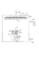
本発明の発光層としての蛍光体薄膜を形成するための装置の構成例の一つを図1に示す。ここでは、硫化バリウムと硫化イットリウムとを含み、さらに発光中心として機能する物質としてのEuが添加された混合ペレットを蒸発源とし、H2Sを導入しつつ、蛍光体薄膜を作製する方法を例にとる。図1において、真空層11内には、発光層としての蛍光体薄膜が形成される基板12と、EB蒸発源14が配置されている。
FIG. 1 shows one configuration example of an apparatus for forming a phosphor thin film as a light emitting layer of the present invention. Here, as an example, a method for producing a phosphor thin film while introducing H 2 S using a mixed pellet containing barium sulfide and yttrium sulfide and further containing Eu as a substance functioning as a luminescence center as an evaporation source is used. To take. In FIG. 1, a
EB蒸発源14は、発光中心として機能する物質が添加されたペレット14aが収納される”るつぼ”40と、電子放出用のフィラメント41aを内蔵した電子銃41とを有する。
The
なお、図示例では、説明を容易にするために蒸発源14の配置が基板に対して偏在しているようにもみえるが、実際には蒸着される蛍光体薄膜の組成および膜厚が均一となるような位置に配置される。
In the illustrated example, the arrangement of the
真空槽11は、排気ポート11aを有し、この排気ポート11aからの排気により、真空槽11内を所定の真空度にできるようになっている。また、この真空槽11は、硫化水素などのガスを導入する原料ガス導入ポート11bを有している。
The
基板12は基板ホルダー12aに固定され、この基板ホルダー12aの固定軸12bは図示しない回転軸固定手段により、真空槽11内の真空度を維持しつつ、外部から回転自在に固定されている。そして、図示しない回転手段により、必要に応じて所定の回転数で基板12を回転可能なようになっている。また、基板ホルダー12aには、ヒーター線などにより構成される加熱手段13が密着・固定されていて、基板12を所望の温度に加熱、保持できるようになっている。
The
このような装置を用い、EB蒸発源14から蒸発させた材料を基板12上に堆積結合させ、Eu添加カルシウムイットレート等の蛍光体薄膜が形成される。そのとき、必要により基板12を回転させることにより、堆積される蛍光体薄膜の組成と膜厚分布をより均一なものとすることができる。
(4) Using such an apparatus, the material evaporated from the
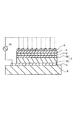
本発明の蛍光体薄膜を用いて無機ELパネルを得るには、例えば、図2に示すような構造とすればよい。 無機 To obtain an inorganic EL panel using the phosphor thin film of the present invention, for example, the structure shown in FIG. 2 may be used.
図2は、本発明の蛍光体薄膜を用いた無機ELパネルの構造の一例を示す一部断面図である。図2において、基板1上にはストライプ状パターンの下部電極5が形成されていて、この下部電極5上に誘電体である下部絶縁層2が形成されている。また、この下部絶縁層2上には、発光層としての蛍光体薄膜3、誘電体である薄膜絶縁層4が順次形成されている。薄膜絶縁層4上には、前記下部電極5とマトリクス回路を構成すべく、下部電極5と交差する方向のストライプ状パターンを有する上部電極6が形成されている。
FIG. 2 is a partial cross-sectional view showing an example of the structure of an inorganic EL panel using the phosphor thin film of the present invention. In FIG. 2, a lower electrode 5 having a stripe pattern is formed on a
下部絶縁層2は、厚膜の誘電体である厚膜絶縁層2aと、この厚膜絶縁層2aの表面を平坦化するための平坦化層として、ゾルゲル法やMOD法など溶液塗布焼成法により形成された絶縁層2bと、を備えている。なお、下部絶縁層2において絶縁層2bがなくても動作は可能である。この場合、厚膜絶縁層2aを平坦化をすべく、厚膜絶縁層2aの表面が研磨されていることが好ましい。
The lower
また、基板1、下部電極5、上部電極6、厚膜絶縁層2a、絶縁層2b、薄膜絶縁層4のそれぞれの間には、密着性を上げるための層、応力を緩和するための層、反応を防止するバリア層、などの中間層を設けてもよい。
Further, between the
ここで、特に絶縁層2bと蛍光体薄膜3の間にバリア層としてBaTiO3薄膜層を設けることが好ましい。また、場合により基板1、下部電極5、上部電極6、厚膜絶縁層2a、絶縁層2b、薄膜絶縁層4のそれぞれの間にBaTiO3薄膜層を形成しても良い。
Here, it is particularly preferable to provide a BaTiO 3 thin film layer as a barrier layer between the insulating
また、さらに、蛍光体薄膜3をZnS薄膜でサンドイッチすることが好ましく、これにより、蛍光体薄膜の電荷の注入特性、耐電圧特性が向上し、より高輝度なEL素子を得ることができる。ZnS薄膜の膜厚は、30nm〜400nmが好ましく、100〜300nmがより好ましい。 Further, it is preferable that the phosphor thin film 3 is sandwiched by a ZnS thin film, whereby the charge injection characteristics and the withstand voltage characteristics of the phosphor thin film are improved, and an EL device with higher luminance can be obtained. The thickness of the ZnS thin film is preferably from 30 nm to 400 nm, more preferably from 100 to 300 nm.
すなわち、ELパネルは、ZnS薄膜/蛍光体薄膜/ZnS薄膜の構造であることが好ましい。また、ELパネルは、ZnS薄膜/蛍光体薄膜/ZnS薄膜/・・・/蛍光体薄膜/ZnS薄膜のように、ZnS薄膜と蛍光体薄膜とを交互に積層し、かつ、最外層をZnS薄膜とするような構造であってもよい。 That is, the EL panel preferably has a structure of ZnS thin film / phosphor thin film / ZnS thin film. The EL panel has a ZnS thin film and a phosphor thin film alternately laminated as ZnS thin film / phosphor thin film / ZnS thin film /.../ phosphor thin film / ZnS thin film, and the outermost layer is a ZnS thin film. May be used.
また、無機ELパネルの構造は、厚膜絶縁層2aを有さず、蛍光体薄膜3を、例えば、タンタル酸バリウムなどの一対の薄膜誘電体で挟んだ積層構造の両端に薄膜状の電極を形成したものでもよい。
Further, the structure of the inorganic EL panel does not have the thick-
基板として用いる材料は、厚膜絶縁層2aの形成温度、絶縁層2bや薄膜絶縁層4の形成温度、および蛍光体薄膜3の形成温度、蛍光体薄膜3のアニール温度に耐えうる耐熱温度以上のものであり、所定の強度を維持できるものであれば特に限定されるものではない。厚膜絶縁層2aを用いる場合には、融点が600℃以上、好ましくは700℃以上、特に800℃以上の耐熱温度を有する基板を用いる。具体的には、ガラス基板やアルミナ(Al2O3)、フォルステライト(2MgO・SiO2)、ステアタイト(MgO・SiO2)、ムライト(3Al2O3・2SiO2)、ベリリア(BeO)、窒化アルミニウム(AlN)、窒化シリコン(SiN)、炭化シリコン(SiC+BeO)等のセラミック基板、結晶化ガラスなど耐熱性ガラス基板を挙げることができる。これらのなかでも特にアルミナ基板、結晶化ガラスが好ましく、熱伝導性が必要な場合にはベリリア、窒化アルミニウム、炭化シリコン等が好ましい。
The material used for the substrate is not less than the heat-resistant temperature that can withstand the formation temperature of the thick-
また、このほかに、石英、熱酸化シリコンウエハー等、チタン、ステンレス、インコネル、鉄系などの金属基板を用いることもできる。金属等の導電性基板を用いる場合には、基板上に内部に電極を有した厚膜を形成した構造が好ましい。 In addition, a metal substrate of titanium, stainless steel, inconel, iron, or the like, such as quartz or thermally oxidized silicon wafer, can also be used. When a conductive substrate such as a metal is used, a structure in which a thick film having an electrode inside is formed on the substrate is preferable.
厚膜絶縁層2aの材料としては、公知の厚膜誘電体材料を用いることができる。さらに比較的誘電率の大きな材料が好ましい。
公 知 A known thick film dielectric material can be used as the material of the thick
例えばチタン酸鉛系、ニオブ酸鉛系、チタン酸バリウム系等の材料を用いることができる。 For example, materials such as lead titanate, lead niobate, and barium titanate can be used.
厚膜絶縁層2aの抵抗率としては、108Ω・cm以上、特に、1010〜1018Ω・cm程度が好ましい。また比較的高い誘電率を有する物質であることが好ましく、その誘電率εとしては、好ましくはε=100〜10000程度である。厚膜絶縁層2aの膜厚としては、5〜50μmが好ましく、10〜30μmが特に好ましい。
The resistivity of the thick
厚膜絶縁層2aの形成方法は、特に限定されず、10〜50μm厚の膜が比較的容易に得られる方法が良いが、ゾルゲル法、印刷焼成法などが好ましい。
方法 The method of forming the thick-
印刷焼成法による場合には、まず、材料の粒度を適当に揃え、バインダーと混合し、適当な粘度のペーストとする。つづいて、このペーストを基板上にスクリーン印刷法により形成し、乾燥させる。その後、このグリーンシートを適当な温度で焼成し、厚膜絶縁層2aを得る。
In the case of the printing and firing method, first, the particle size of the material is appropriately adjusted, and the material is mixed with a binder to obtain a paste having an appropriate viscosity. Subsequently, this paste is formed on a substrate by a screen printing method and dried. Thereafter, the green sheet is fired at an appropriate temperature to obtain the thick
薄膜絶縁層4の構成材料としては、例えばタンタル酸バリウム(BaTa2O6)、酸化シリコン(SiO2)、窒化シリコン(SiN)、酸化タンタル(Ta2O5)、チタン酸ストロンチウム(SrTiO3)、酸化イットリウム(Y2O3)、チタン酸バリウム(BaTiO3)、チタン酸鉛(PbTiO3)、PZT、ジルコニア(ZrO2)、シリコンオキシナイトライド(SiON)、アルミナ(Al2O3)、ニオブ酸鉛、PMN−PT系材料等およびこれらの多層または混合薄膜を挙げることができ、これらの材料で薄膜絶縁層4を形成する方法としては、蒸着法、スパッタ法、CVD法、ゾルゲル法、印刷焼成法など既存の方法を用いればよい。この場合の薄膜絶縁層4の膜厚としては、好ましくは50〜1000nm、特に100〜500nm程度である。 As a constituent material of the thin film insulating layer 4, for example, barium tantalate (BaTa 2 O 6 ), silicon oxide (SiO 2 ), silicon nitride (SiN), tantalum oxide (Ta 2 O 5 ), strontium titanate (SrTiO 3 ) , Yttrium oxide (Y 2 O 3 ), barium titanate (BaTiO 3 ), lead titanate (PbTiO 3 ), PZT, zirconia (ZrO 2 ), silicon oxynitride (SiON), alumina (Al 2 O 3 ), Lead niobate, PMN-PT-based materials and the like and multilayers or mixed thin films thereof can be mentioned. Methods for forming the thin film insulating layer 4 with these materials include a vapor deposition method, a sputtering method, a CVD method, a sol-gel method, An existing method such as a printing and baking method may be used. In this case, the thickness of the thin-film insulating layer 4 is preferably 50 to 1000 nm, particularly about 100 to 500 nm.
下部電極5は、少なくとも基板1上または厚膜絶縁層2a内に形成される。厚膜絶縁層2aの形成時や、さらに蛍光体薄膜の熱処理時に高温下にさらされる下部電極5は、主成分としてパラジウム、ロジウム、イリジウム、レニウム、ルテニウム、白金、タンタル、ニッケル、クロム、チタン等の1種または2種以上の金属を含む通常用いられている金属電極を用いればよい。厚膜絶縁層2aを用いず一対の薄膜誘電体で蛍光体薄膜3を挟みこんだEL素子の場合は、下部電極5にはZnOやITOなどの透明電極を用いることができる。
The lower electrode 5 is formed at least on the
また、上部電極6としては、通常、発光を基板と反対側から取り出すため、所定の発光波長域で透光性を有する透明電極であることが好ましい。なお、基板1および厚膜絶縁層2が透光性を有するものである場合は、発光光を基板1側から取り出すべく、下部電極5を透明電極としてもよい。
In addition, the
透明電極としては、ZnO、ITOなどを用いることが特に好ましい。ITOは、通常In2O3とSnOとを化学量論組成で含有するが、O量は多少これから偏倚していてもよい。In2O3に対するSnO2の混合比は、1〜20質量%、さらには5〜12質量%が好ましい。また、IZOでのIn2O3に対するZnOの混合比は、通常、12〜32質量%程度である。 It is particularly preferable to use ZnO, ITO, or the like as the transparent electrode. ITO usually contains In 2 O 3 and SnO in a stoichiometric composition, but the amount of O may slightly deviate from this. The mixing ratio of SnO 2 to In 2 O 3 is preferably 1 to 20% by mass, more preferably 5 to 12% by mass. The mixing ratio of ZnO to In 2 O 3 in IZO is usually about 12 to 32% by mass.
また、これらの電極は、シリコンを有するものでも良い。このシリコン電極層は、多結晶シリコン(p−Si)であっても、アモルファス(a−Si)であってもよく、必要により単結晶シリコンであってもよい。 電極 These electrodes may include silicon. This silicon electrode layer may be polycrystalline silicon (p-Si) or amorphous (a-Si), and may be single crystal silicon if necessary.
シリコンを有する電極は、主成分のシリコンに加え、導電性を確保するため物質をドーピングする。物質として用いられるドーパントは、所定の導電性を確保しうるものであればよく、シリコン半導体に用いられている通常のドーパントを用いることができる。具体的には、B、P、As、Sb、Al等が挙げられ、これらのなかでも、特にB、P、As、SbおよびAlが好ましい。ドーパントの濃度としては0.001〜5原子%程度が好ましい。 電極 An electrode containing silicon is doped with a substance in order to secure conductivity in addition to silicon as a main component. The dopant used as the substance may be any as long as it can secure predetermined conductivity, and a normal dopant used for a silicon semiconductor can be used. Specific examples include B, P, As, Sb, and Al. Among them, B, P, As, Sb, and Al are particularly preferable. The concentration of the dopant is preferably about 0.001 to 5 atomic%.
これらの材料で電極層を形成する方法としては、蒸着法、スパッタ法、CVD法、ゾルゲル法、印刷焼成法など既存の方法を用いればよいが、特に、基板1上に内部に下部電極5を有した厚膜絶縁層2aを形成した構造を作製する場合、厚膜絶縁層2aの形成と同じ方法で電極層を形成することが好ましい。
As a method for forming an electrode layer using these materials, an existing method such as a vapor deposition method, a sputtering method, a CVD method, a sol-gel method, and a printing and baking method may be used. In particular, the lower electrode 5 is formed inside the
上部・下部電極層4、5の好ましい抵抗率としては、発光層3に効率よく電界を付与するため、1Ω・cm以下、特に0.003〜0.1Ω・cmが好ましい。これらの電極層の膜厚としては、形成する材料にもよるが、好ましくは50〜2000nm、特に100〜1000nm程度が好ましい。 (4) The preferable resistivity of the upper and lower electrode layers 4 and 5 is 1 Ω · cm or less, particularly 0.003 to 0.1 Ω · cm, in order to efficiently apply an electric field to the light emitting layer 3. The thickness of these electrode layers depends on the material to be formed, but is preferably from 50 to 2000 nm, particularly preferably from about 100 to 1000 nm.
以上、Ca1Y2S4:Eu蛍光体薄膜を用いたELパネルについて、説明したが、本発明において元素AはCaに限定されるものではなく、Mg、Ca、Sr、BaおよびZnのいずれか1種または2種以上であればよい。また、元素BもYに限定されるものではなく、上述の希土類元素の何れか1種または2種以上であればよい。 As described above, the EL panel using the Ca 1 Y 2 S 4 : Eu phosphor thin film has been described. However, in the present invention, the element A is not limited to Ca, and may be any of Mg, Ca, Sr, Ba, and Zn. Or at least one type. Further, the element B is not limited to Y, but may be any one or more of the above-mentioned rare earth elements.
ここで、元素Aとして、Ca以外のMg、Sr、Ba、Znの元素を用いる場合には、これらの硫化物や酸化物を含むペレットを用いればよい。また、元素Bとして、Y以外の希土類元素を用いる場合も、Y以外の希土類元素の硫化物、酸化物等を含むペレットを用いればよい。 Here, when elements other than Ca, such as Mg, Sr, Ba, and Zn, are used as the element A, pellets containing these sulfides and oxides may be used. When a rare earth element other than Y is used as the element B, a pellet containing a sulfide, an oxide, or the like of a rare earth element other than Y may be used.
さらに、発光中心として機能する物質もEuでなく、Euの化合物でもよく、Ceやその化合物、Mnやその化合物等を用いても良い。この場合も、これらの金属や、金属の酸化物、硫化物等を含むペレットを用いればよい。 物質 Furthermore, the substance functioning as the luminescence center is not Eu, but may be a compound of Eu, or Ce or its compound, Mn or its compound, or the like. Also in this case, pellets containing these metals, metal oxides, sulfides, and the like may be used.
さらに、母対材料が硫黄を含まない、すなわち、z=0の蛍光体薄膜を作製するためには、電子ビーム蒸着装置の真空層内にH2Sガスを導入せず、かつ、アニール時にもH2Sガスを導入しなければよい。この場合、例えば、CaY2O4:Euであれば、CaO、Y2O3、Eu2O3等を含むペレットによる電子ビーム蒸着や、CaO、Y2O3の混合ペレット及びEu2O3のペレットを用いた2元蒸着法を利用できる。 Furthermore, in order to produce a phosphor thin film in which the matrix material does not contain sulfur, that is, z = 0, H 2 S gas is not introduced into the vacuum layer of the electron beam evaporation apparatus, and at the time of annealing. H 2 S gas need not be introduced. In this case, for example, in the case of CaY 2 O 4 : Eu, electron beam evaporation using a pellet containing CaO, Y 2 O 3 , Eu 2 O 3, etc., a mixed pellet of CaO, Y 2 O 3 and Eu 2 O 3 A binary vapor deposition method using the above-mentioned pellets can be used.
そして、このようなELパネルの発光層3において、RGBの3色に対応する蛍光体薄膜を並設することにより、フルカラーELパネルが得られる。 {Circle around (2)} By providing phosphor thin films corresponding to the three colors of RGB in the light emitting layer 3 of such an EL panel, a full-color EL panel can be obtained.
このようなELパネルは、主にディスプレイ用のフルカラーパネル、マルチカラーパネル、部分的に3色を表示するパーシャリーカラーパネルに応用することができる。 (5) Such an EL panel can be mainly applied to a full-color panel for display, a multi-color panel, and a partially-color panel for partially displaying three colors.
以下、本発明の具体的実施例を示し、本発明をさらに詳細に説明する。 Hereinafter, specific examples of the present invention will be shown, and the present invention will be described in more detail.
〔実施例1〕
本発明の蛍光体薄膜を用いたELパネル(EL素子)を作製した。ガラス基板上にITO透明電極を100nmスパッタリング法により形成し、この上にタンタル酸バリウム薄膜誘電体をスパッタリング法により300nm形成した。この上に、EL薄膜/タンタル酸バリウム薄膜(200nm)の構造体を作製した。EL薄膜は、ZnS膜(200nm)/蛍光体薄膜(300nm)/ZnS膜(200nm)の構造とした。
[Example 1]
An EL panel (EL element) using the phosphor thin film of the present invention was produced. An ITO transparent electrode was formed on a glass substrate by 100 nm by a sputtering method, and a barium tantalate thin film dielectric was formed thereon by 300 nm by a sputtering method. An EL thin film / barium tantalate thin film (200 nm) structure was formed thereon. The EL thin film had a structure of ZnS film (200 nm) / phosphor thin film (300 nm) / ZnS film (200 nm).
蛍光体薄膜の作製にあたって、以下のような電子ビーム蒸着法を用いた。 電子 The following electron beam evaporation method was used for producing the phosphor thin film.
Euを0.5mol%添加したCa1Y2S4ペレットを入れたEB源をH2Sガスを導入した真空槽内に設け、この源より所定の蒸発速度でペレットを蒸発させ、400℃に加熱し回転させた基板上に蛍光体薄膜を成膜した。蒸発源の蒸発速度は、基板上に成膜される膜の成膜速度が1nm/secになるように調節した。このときH2Sガスを20SCCM導入し、蛍光体薄膜を得た。 An EB source containing Ca 1 Y 2 S 4 pellets containing 0.5 mol% of Eu is provided in a vacuum chamber into which H 2 S gas is introduced, and the pellets are evaporated from the source at a predetermined evaporation rate. A phosphor thin film was formed on the heated and rotated substrate. The evaporation rate of the evaporation source was adjusted so that the film formation rate of the film formed on the substrate was 1 nm / sec. At this time, 20 SCCM of H 2 S gas was introduced to obtain a phosphor thin film.
このようにして、BaTa2O6膜(200nm)/ZnS膜(200nm)/蛍光体薄膜(400nm)/ZnS膜(200nm)/BaTa2O6膜(300nm)/透明電極(100nm)/基板の構造の積層体を得た後、700℃のアルゴン中で10分間アニールした。 Thus, the BaTa 2 O 6 film (200 nm) / ZnS film (200 nm) / phosphor thin film (400 nm) / ZnS film (200 nm) / BaTa 2 O 6 film (300 nm) / transparent electrode (100 nm) / substrate After obtaining the laminate having the structure, the laminate was annealed in argon at 700 ° C. for 10 minutes.
さらに、得られた積層体上にITO酸化物ターゲットを用いRFマグネトロンスパッタリング法により、基板温度250℃で、膜厚200nmのITO透明電極を形成し、ELパネルを完成した。 {Circle around (2)} An ITO transparent electrode having a thickness of 200 nm was formed on the obtained laminate by RF magnetron sputtering using an ITO oxide target at a substrate temperature of 250 ° C. to complete an EL panel.
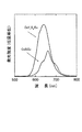
得られたELパネルの2つの電極間に1kHz、パルス幅50μSの電界を印加することにより、400cd/m2、CIE 1931色度図で(0.67,0.33)のNTSCレベルの赤色発光輝度が再現良く得られた。本ELパネルでは、電圧を印加してから発光が安定するまでの応答時間が、従来例では数秒から数十秒であったものが、20ms以下まで向上していた。図3に発光スペクトルを、図4にL−V特性を示す。従来に較べ、高輝度のELパネルが得られることがわかる。 By applying an electric field of 1 kHz and a pulse width of 50 μS between the two electrodes of the obtained EL panel, red light emission of 400 cd / m 2 and NTSC level of (0.67, 0.33) in the CIE 1931 chromaticity diagram was obtained. Brightness was obtained with good reproducibility. In the present EL panel, the response time from application of a voltage to stabilization of light emission has been improved from several seconds to several tens of seconds in the conventional example to 20 ms or less. FIG. 3 shows the emission spectrum, and FIG. 4 shows the LV characteristics. It can be seen that an EL panel having a higher luminance can be obtained as compared with the related art.
ここで、蛍光体薄膜の組成を蛍光X線分析により調べたところ、各元素のモル比は、Ca:Y:S:Eu=10.36:29.24:43.49:0.57であった。 When the composition of the phosphor thin film was examined by X-ray fluorescence analysis, the molar ratio of each element was Ca: Y: S: Eu = 10.36: 29.24: 43.49: 0.57. Was.
〔比較例1〕
蛍光体薄膜を、従来赤色EL材料として優れていると言われているCaS:Euとする以外は、実施例1と同様にしてELパネルを得た。得られたELパネルの発光輝度は、1kHz駆動で80cd/m2程度であり、かつ、電圧を印加してから発光が安定するまでの応答時間が、数秒から数十秒であり、カラーディスプレイのELパネルとするためには、より高輝度化と応答性の改善が必要であった。発光スペクトルを図3に示す。
[Comparative Example 1]
An EL panel was obtained in the same manner as in Example 1, except that the phosphor thin film was CaS: Eu, which is conventionally considered to be excellent as a red EL material. The emission luminance of the obtained EL panel is about 80 cd / m 2 when driven at 1 kHz, and the response time from application of a voltage to stabilization of light emission is several seconds to several tens of seconds. In order to obtain an EL panel, higher luminance and improved responsiveness were required. FIG. 3 shows the emission spectrum.
〔実施例2〕
実施例1において、蛍光体薄膜の材料をCa1Y2S4:Euから種々のイットレート蛍光体に変えることにより各種のELパネルを作製した。具体的には、各イットレート蛍光体をBa1Y2S4:Eu、Sr1Y2S4:Eu、Ba1Y2S4:Mn、Sr1Y2S4:Mn、Mg1Y2S4:Mn、Zn1Y2S4:Mnとした。これらのチオイットレート蛍光体を用いたELパネルの発光ピーク波長とCIE 1931色度値とを表1に示す。ここで、発光ピーク波長及び色度値についてはPL(Photo Luminescence)スペクトルから算出した。各蛍光体薄膜のPLスペクトルの測定結果を図5,6に示す。

In Example 1, various EL panels were manufactured by changing the material of the phosphor thin film from Ca 1 Y 2 S 4 : Eu to various yttrate phosphors. Specifically, each IT rate phosphors Ba 1 Y 2 S 4: Eu , Sr 1 Y 2 S 4: Eu, Ba 1 Y 2 S 4: Mn, Sr 1 Y 2 S 4: Mn, Mg 1 Y 2 S 4 : Mn and Zn 1 Y 2 S 4 : Mn. Table 1 shows emission peak wavelengths and CIE 1931 chromaticity values of EL panels using these thioytrate phosphors. Here, the emission peak wavelength and the chromaticity value were calculated from a PL (Photo Luminescence) spectrum. Measurement results of the PL spectrum of each phosphor thin film are shown in FIGS.
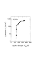
また、PLスペクトルの結果から、特にSr1Y2S4:Euからきわめて色純度の良い高輝度赤色発光が得られ、Ba1Y2S4:Mnから高輝度な青色発光が得られたのがわかる。Sr1Y2S4:Euの電圧−輝度特性を図7に示す。 Also, from the results of the PL spectrum, high luminance red light emission with extremely good color purity was obtained especially from Sr 1 Y 2 S 4 : Eu, and high luminance blue light emission was obtained from Ba 1 Y 2 S 4 : Mn. I understand. FIG. 7 shows the voltage-luminance characteristics of Sr 1 Y 2 S 4 : Eu.
さらに、ZnY2S4:Mnからはきわめて色純度の良い緑色の高輝度発光が得られた。 Further, from ZnY 2 S 4 : Mn, green high-luminance emission with extremely good color purity was obtained.
なお、実施例1で得られたCa1Y2S4:EuのELパネルについてのPLスペクトルも図5に、このPLスペルトルにより得られた実施例1のELパネルの発光ピーク波長及び色度値についても表1に各々示す。 The PL spectrum of the EL panel of Ca 1 Y 2 S 4 : Eu obtained in Example 1 is also shown in FIG. 5, and the emission peak wavelength and chromaticity value of the EL panel of Example 1 obtained by this PL spectrum are shown. Are also shown in Table 1.
これによって、Ca,Ba,Sr,Mgからなるアルカリ土類金属やZnと、イットリウムと、を含む複合硫化物に、発光中心として機能する物質を添加した蛍光体薄膜は、従来に比してきわめて高輝度に発光することが確認された。ここで、イットリウムに代えて、イットリウムと同様の性質を有する他の希土類金属を添加しても、同様の効果があるものと類推される。 As a result, a phosphor thin film in which a substance functioning as a luminescent center is added to a complex sulfide containing an alkaline earth metal or Zn made of Ca, Ba, Sr, and Mg and yttrium, as compared with the related art. It was confirmed that light was emitted with high luminance. Here, it is presumed that the same effect is obtained by adding another rare earth metal having the same properties as yttrium instead of yttrium.
〔実施例3〕
実施例1において、蛍光体薄膜の材料をCa1Y2S4:EuからCa1Y2O2S2:Eu蛍光体に代えたELパネルを作製した。
[Example 3]
In Example 1, an EL panel was manufactured in which the material of the phosphor thin film was changed from Ca 1 Y 2 S 4 : Eu to Ca 1 Y 2 O 2 S 2 : Eu phosphor.
具体的には、CaS、Y2S3、Y2O3、Eu2S3を含むターゲットを用いて蒸着法により形成した。図8に、ELパネルの発光スペクトルを示す。この蛍光体も、実施例1と同様の輝度及び応答性を示した。 Specifically, it was formed by an evaporation method using a target containing CaS, Y 2 S 3 , Y 2 O 3 , and Eu 2 S 3 . FIG. 8 shows an emission spectrum of the EL panel. This phosphor also exhibited the same luminance and responsiveness as in Example 1.
〔実施例4〕
実施例1の蛍光体薄膜を用いて厚膜絶縁層を有するELパネル(EL素子)を作製した。基板、厚膜絶縁体層とも同じ材料であるBaTiO3系の誘電体材料(誘電率ε:5000)を用い、下部電極としてPd電極を用いた。
[Example 4]
Using the phosphor thin film of Example 1, an EL panel (EL element) having a thick film insulating layer was manufactured. A BaTiO 3 -based dielectric material (dielectric constant ε: 5000), which is the same material for both the substrate and the thick insulator layer, was used, and a Pd electrode was used as the lower electrode.
まず、基板のシートを作製し、この上に下部電極、厚膜絶縁層をスクリーン印刷してグリーンシートとし、同時に焼成した。得られた複合基板の表面を研磨し、30μm厚の厚膜絶縁層付き基板を得た。さらに、この上にバリア層としてBaTiO3膜をスパッタリング法により膜厚400nmに形成し、700℃の空気中でアニールし、複合基板とした。 First, a substrate sheet was prepared, and a lower electrode and a thick film insulating layer were screen-printed thereon to form a green sheet, which was simultaneously fired. The surface of the obtained composite substrate was polished to obtain a substrate with a thick insulating layer having a thickness of 30 μm. Further, a BaTiO 3 film was formed thereon as a barrier layer to a thickness of 400 nm by a sputtering method, and annealed in air at 700 ° C. to obtain a composite substrate.
この複合基板上に、ELパネルとして安定に発光させるため、Al2O3膜(50nm)/EL薄膜/Al2O3膜(50nm)の構造体を作製した。EL薄膜は、ZnS膜(200nm)/蛍光体薄膜(300nm)/ZnS膜(200nm)の構造とした。 On this composite substrate, a structure of an Al 2 O 3 film (50 nm) / EL thin film / Al 2 O 3 film (50 nm) was manufactured to stably emit light as an EL panel. The EL thin film had a structure of ZnS film (200 nm) / phosphor thin film (300 nm) / ZnS film (200 nm).
蛍光体薄膜の作製にあたって、実施例1と同様にCa1Y2S4:Eu薄膜を作製して用いた。 In preparing the phosphor thin film, a Ca 1 Y 2 S 4 : Eu thin film was prepared and used in the same manner as in Example 1.
得られた積層薄膜は、Al2O3膜(50nm)/ZnS膜(200nm)/蛍光体薄膜(300nm)/ZnS膜(200nm)/Al2O3膜(50nm)の構造にしてから、700℃の空気中で10分間アニールした。 The obtained laminated thin film has a structure of Al 2 O 3 film (50 nm) / ZnS film (200 nm) / phosphor thin film (300 nm) / ZnS film (200 nm) / Al 2 O 3 film (50 nm) and then 700 Annealed in air at 10 ° C. for 10 minutes.
さらに、得られた積層薄膜上にITO酸化物ターゲットを用いRFマグネトロンスパッタリング法により、基板温度250℃で、膜厚200nmのITO透明電極を形成し、ELパネルを完成した。 Furthermore, an ITO transparent electrode having a thickness of 200 nm was formed on the obtained laminated thin film at a substrate temperature of 250 ° C. using an ITO oxide target by RF magnetron sputtering, thereby completing an EL panel.
得られたELパネルの2つの電極間に1kHz、パルス幅50μSの電界を印加することにより、500cd/m2、CIE 1931色度図で(0.67,0.33)の赤色発光輝度が得られた。本EL素子では、応答性が比較例1で、数秒から数十秒であったものが、20ms以下まで向上していた。従来の赤色材料であるCaS:Euを用いた比較例1のELパネルでは80cd/m2程度であったものに対して高輝度のEL素子が得られることがわかる。 By applying an electric field of 1 kHz and a pulse width of 50 μS between the two electrodes of the obtained EL panel, a red emission luminance of (0.67, 0.33) is obtained in the CIE 1931 chromaticity diagram at 500 cd / m 2 . Was done. In this EL device, the response was from several seconds to several tens of seconds in Comparative Example 1, but was improved to 20 ms or less. It can be seen that the EL panel of Comparative Example 1 using CaS: Eu, which is a conventional red material, can provide a high-brightness EL element compared to about 80 cd / m 2 .
以上の実施例から明らかなように本発明の蛍光体薄膜を有するELパネルは、高輝度に発光する。 よ う As is clear from the above examples, the EL panel having the phosphor thin film of the present invention emits light with high luminance.
このような蛍光体薄膜を用いたELパネルを利用することにより、特に、輝度の高い多色ELパネルやフルカラーELパネルを実現でき、実用的価値は大きい。 多 By using an EL panel using such a phosphor thin film, a multi-color EL panel or a full-color EL panel with high luminance can be realized, and its practical value is great.
1…基板、2…下部絶縁層、2a…厚膜絶縁体層、2b…溶液塗布焼成法により形成された絶縁層、3…蛍光体薄膜(発光層)、4…薄膜絶縁体層、5…下部電極、6…上部電極(透明電極)。
DESCRIPTION OF
Claims (7)
AxByOwSz
[但し、AはMg、Ca、Sr、BaおよびZnからなる群から選ばれた少なくとも一つの元素、BはSc、Y、La、Ce、Pr、Nd、Pm、Sm、Eu、Gd、Tb、Dy、Ho、Er、Tm、Yb及びLuからなる群から選ばれた少なくとも一つの元素を表し、0<x<5、0<y<4、0≦z<8、0≦w<8であり、0=z=wとなることはない。]
この母材に対し発光中心として機能する物質が含有されている蛍光体薄膜。 Having a base material represented by the following composition formula,
A x B y O w S z
[Where A is at least one element selected from the group consisting of Mg, Ca, Sr, Ba and Zn, B is Sc, Y, La, Ce, Pr, Nd, Pm, Sm, Eu, Gd, Tb, Represents at least one element selected from the group consisting of Dy, Ho, Er, Tm, Yb, and Lu, where 0 <x <5, 0 <y <4, 0 ≦ z <8, and 0 ≦ w <8. , 0 = z = w. ]
A phosphor thin film containing a substance functioning as a luminescent center with respect to the base material.
Priority Applications (2)
| Application Number | Priority Date | Filing Date | Title |
|---|---|---|---|
| JP2003326736A JP2004137480A (en) | 2002-09-20 | 2003-09-18 | Fluorescent substance thin film, method for producing the same and el panel |
| US10/664,923 US6939482B2 (en) | 2002-09-20 | 2003-09-22 | Phosphor thin film, manufacturing method of the same, and electroluminescent panel |
Applications Claiming Priority (2)
| Application Number | Priority Date | Filing Date | Title |
|---|---|---|---|
| JP2002274516 | 2002-09-20 | ||
| JP2003326736A JP2004137480A (en) | 2002-09-20 | 2003-09-18 | Fluorescent substance thin film, method for producing the same and el panel |
Publications (2)
| Publication Number | Publication Date |
|---|---|
| JP2004137480A true JP2004137480A (en) | 2004-05-13 |
| JP2004137480A5 JP2004137480A5 (en) | 2005-08-04 |
Family
ID=32473024
Family Applications (1)
| Application Number | Title | Priority Date | Filing Date |
|---|---|---|---|
| JP2003326736A Pending JP2004137480A (en) | 2002-09-20 | 2003-09-18 | Fluorescent substance thin film, method for producing the same and el panel |
Country Status (2)
| Country | Link |
|---|---|
| US (1) | US6939482B2 (en) |
| JP (1) | JP2004137480A (en) |
Cited By (2)
| Publication number | Priority date | Publication date | Assignee | Title |
|---|---|---|---|---|
| WO2006129593A1 (en) * | 2005-06-03 | 2006-12-07 | Kabushiki Kaisha Toshiba | Phosphor for display and field emission display |
| JP2009132932A (en) * | 2008-12-24 | 2009-06-18 | National Institute Of Advanced Industrial & Technology | Phosphor having crystallized metal oxide membrane |
Families Citing this family (23)
| Publication number | Priority date | Publication date | Assignee | Title |
|---|---|---|---|---|
| US7812522B2 (en) * | 2004-07-22 | 2010-10-12 | Ifire Ip Corporation | Aluminum oxide and aluminum oxynitride layers for use with phosphors for electroluminescent displays |
| WO2006045195A1 (en) * | 2004-10-29 | 2006-05-04 | Ifire Technology Corp. | Novel thiosilicate phosphor compositions and deposition methods using barium-silicon vacuum deposition sources for deposition of thiosilicate phosphor films |
| JP2006140083A (en) * | 2004-11-15 | 2006-06-01 | Tohoku Univ | Fluorescent lamp |
| US7484315B2 (en) * | 2004-11-29 | 2009-02-03 | Tokyo Electron Limited | Replaceable precursor tray for use in a multi-tray solid precursor delivery system |
| US7488512B2 (en) * | 2004-11-29 | 2009-02-10 | Tokyo Electron Limited | Method for preparing solid precursor tray for use in solid precursor evaporation system |
| US7638002B2 (en) * | 2004-11-29 | 2009-12-29 | Tokyo Electron Limited | Multi-tray film precursor evaporation system and thin film deposition system incorporating same |
| US7708835B2 (en) * | 2004-11-29 | 2010-05-04 | Tokyo Electron Limited | Film precursor tray for use in a film precursor evaporation system and method of using |
| KR100730122B1 (en) * | 2004-12-24 | 2007-06-19 | 삼성에스디아이 주식회사 | Yttrium based phosphors comprising a conductive material, the process for preparing the same, and the display device using the same |
| US7651570B2 (en) * | 2005-03-31 | 2010-01-26 | Tokyo Electron Limited | Solid precursor vaporization system for use in chemical vapor deposition |
| WO2007086310A1 (en) * | 2006-01-27 | 2007-08-02 | Semiconductor Energy Laboratory Co., Ltd. | Light emitting material, light emitting device, and electronic device |
| WO2007086311A1 (en) * | 2006-01-27 | 2007-08-02 | Semiconductor Energy Laboratory Co., Ltd. | Light-emitting material, light-emitting element, light-emitting device, and electronic appliance |
| WO2007091500A1 (en) * | 2006-02-10 | 2007-08-16 | Semiconductor Energy Laboratory Co., Ltd. | Light emitting element, light emitting device, and electronic device |
| US20070190235A1 (en) * | 2006-02-10 | 2007-08-16 | Semiconductor Energy Laboratory Co., Ltd. | Film forming apparatus, film forming method, and manufacturing method of light emitting element |
| US20070190675A1 (en) * | 2006-02-10 | 2007-08-16 | Semiconductor Energy Laboratory Co., Ltd. | Manufacturing method of display device |
| US20070194321A1 (en) * | 2006-02-17 | 2007-08-23 | Semiconductor Energy Laboratory Co., Ltd. | Light emitting element, light emitting device, and electronic device |
| EP1821579A3 (en) * | 2006-02-17 | 2008-04-02 | Semiconductor Energy Laboratory Co., Ltd. | Light emitting element, light emitting device, and electronic appliance |
| WO2007100020A1 (en) * | 2006-03-02 | 2007-09-07 | Semiconductor Energy Laboratory Co., Ltd. | Light-emitting element, light-emitting device, lighting device, and electronic appliance |
| WO2007108390A1 (en) | 2006-03-21 | 2007-09-27 | Semiconductor Energy Laboratory Co., Ltd. | Light-emitting element, display device, and electronic appliance |
| US20070281574A1 (en) * | 2006-06-01 | 2007-12-06 | Semiconductor Energy Laboratory Co., Ltd. | Method for manufacturing electroluminescent material |
| US20080012027A1 (en) * | 2006-07-13 | 2008-01-17 | Semiconductor Energy Laboratory Co., Ltd. | Light-emitting element, light-emitting device, and method of fabricating light-emitting element |
| US7846256B2 (en) * | 2007-02-23 | 2010-12-07 | Tokyo Electron Limited | Ampule tray for and method of precursor surface area |
| DE102010017438A1 (en) * | 2010-06-17 | 2011-12-22 | Paul Hettich Gmbh & Co. Kg | Component, in particular for a fitting, a furniture and / or a household appliance, method for producing a component, fitting, furniture and / or household appliance |
| CN103094159B (en) * | 2011-10-31 | 2016-02-24 | 细美事有限公司 | Substrate processing apparatus and substrate processing method using same |
Family Cites Families (8)
| Publication number | Priority date | Publication date | Assignee | Title |
|---|---|---|---|---|
| JPH01206594A (en) | 1987-10-14 | 1989-08-18 | Komatsu Ltd | Film type el element and its manufacture |
| JPH0251891A (en) | 1988-08-12 | 1990-02-21 | Hitachi Ltd | Thin film el element |
| JPH02148688A (en) | 1988-11-30 | 1990-06-07 | Sumitomo Metal Ind Ltd | Thin film el element |
| US5309070A (en) | 1991-03-12 | 1994-05-03 | Sun Sey Shing | AC TFEL device having blue light emitting thiogallate phosphor |
| JP2840185B2 (en) | 1993-10-21 | 1998-12-24 | 松下電器産業株式会社 | Phosphor thin film and thin film EL panel using the same |
| JP3590986B2 (en) | 1994-03-22 | 2004-11-17 | 株式会社デンソー | Electroluminescence element |
| US6042746A (en) * | 1997-01-17 | 2000-03-28 | Micron Technology, Inc. | Specialized phosphors prepared by a multi-stage grinding and firing sequence |
| US6252254B1 (en) * | 1998-02-06 | 2001-06-26 | General Electric Company | Light emitting device with phosphor composition |
-
2003
- 2003-09-18 JP JP2003326736A patent/JP2004137480A/en active Pending
- 2003-09-22 US US10/664,923 patent/US6939482B2/en not_active Expired - Fee Related
Cited By (2)
| Publication number | Priority date | Publication date | Assignee | Title |
|---|---|---|---|---|
| WO2006129593A1 (en) * | 2005-06-03 | 2006-12-07 | Kabushiki Kaisha Toshiba | Phosphor for display and field emission display |
| JP2009132932A (en) * | 2008-12-24 | 2009-06-18 | National Institute Of Advanced Industrial & Technology | Phosphor having crystallized metal oxide membrane |
Also Published As
| Publication number | Publication date |
|---|---|
| US20040206935A1 (en) | 2004-10-21 |
| US6939482B2 (en) | 2005-09-06 |
Similar Documents
| Publication | Publication Date | Title |
|---|---|---|
| JP2004137480A (en) | Fluorescent substance thin film, method for producing the same and el panel | |
| JP3704068B2 (en) | EL panel | |
| JP3704057B2 (en) | Phosphor thin film and method for manufacturing the same, and EL panel | |
| JP2003238953A (en) | Phosphor and el panel | |
| JP3479273B2 (en) | Phosphor thin film manufacturing method and EL panel | |
| US7011896B2 (en) | Phosphor thin film, preparation method, and EL panel | |
| JP4230363B2 (en) | Phosphor thin film, manufacturing method thereof, and EL panel | |
| US6627251B2 (en) | Phosphor thin film, preparation method, and EL panel | |
| EP1207722B1 (en) | EL phosphor multilayer thin film device | |
| US6761835B2 (en) | Phosphor multilayer and EL panel | |
| US20020192500A1 (en) | Phosphor thin film, preparation method, and EL panel | |
| JP4199673B2 (en) | EL phosphor laminated thin film and EL element | |
| US6821647B2 (en) | Phosphor thin film preparation method, and EL panel | |
| JP4230164B2 (en) | Phosphor thin film, manufacturing method thereof, and EL panel | |
| JP2003055651A (en) | Phosphor thin film and el panel | |
| JP4206221B2 (en) | EL phosphor laminated thin film and EL element | |
| JP3501742B2 (en) | Multilayer phosphor and EL panel | |
| JP2003332081A (en) | El fluorescent material laminated thin film and el element | |
| JP2003272848A (en) | Manufacturing method of phosphor thin film and el panel | |
| JP2002201468A (en) | Phosphor thin film, its preparation process and el panel | |
| JP2003301170A (en) | Phosphor thin film, production process therefor, and el panel | |
| JP2003003161A (en) | Phosphor thin film, method for producing the same and el panel | |
| KR20030011892A (en) | Phosphor Thin Film, Its Production Method, and EL Panel | |
| JP2003201471A (en) | Fluorescent thin film and el panel |
Legal Events
| Date | Code | Title | Description |
|---|---|---|---|
| A521 | Request for written amendment filed |
Free format text: JAPANESE INTERMEDIATE CODE: A523 Effective date: 20050225 |
|
| A621 | Written request for application examination |
Free format text: JAPANESE INTERMEDIATE CODE: A621 Effective date: 20050225 |
|
| A871 | Explanation of circumstances concerning accelerated examination |
Free format text: JAPANESE INTERMEDIATE CODE: A871 Effective date: 20050225 |
|
| A975 | Report on accelerated examination |
Free format text: JAPANESE INTERMEDIATE CODE: A971005 Effective date: 20050331 |
|
| A977 | Report on retrieval |
Free format text: JAPANESE INTERMEDIATE CODE: A971007 Effective date: 20050628 |
|
| A131 | Notification of reasons for refusal |
Free format text: JAPANESE INTERMEDIATE CODE: A131 Effective date: 20050705 |
|
| A02 | Decision of refusal |
Free format text: JAPANESE INTERMEDIATE CODE: A02 Effective date: 20060104 |