JP2004126486A - Device and method for correcting pattern size - Google Patents
Device and method for correcting pattern size Download PDFInfo
- Publication number
- JP2004126486A JP2004126486A JP2002322899A JP2002322899A JP2004126486A JP 2004126486 A JP2004126486 A JP 2004126486A JP 2002322899 A JP2002322899 A JP 2002322899A JP 2002322899 A JP2002322899 A JP 2002322899A JP 2004126486 A JP2004126486 A JP 2004126486A
- Authority
- JP
- Japan
- Prior art keywords
- pattern
- aperture ratio
- correction
- correcting
- test
- Prior art date
- Legal status (The legal status is an assumption and is not a legal conclusion. Google has not performed a legal analysis and makes no representation as to the accuracy of the status listed.)
- Pending
Links
Images
Classifications
-
- G—PHYSICS
- G03—PHOTOGRAPHY; CINEMATOGRAPHY; ANALOGOUS TECHNIQUES USING WAVES OTHER THAN OPTICAL WAVES; ELECTROGRAPHY; HOLOGRAPHY
- G03F—PHOTOMECHANICAL PRODUCTION OF TEXTURED OR PATTERNED SURFACES, e.g. FOR PRINTING, FOR PROCESSING OF SEMICONDUCTOR DEVICES; MATERIALS THEREFOR; ORIGINALS THEREFOR; APPARATUS SPECIALLY ADAPTED THEREFOR
- G03F1/00—Originals for photomechanical production of textured or patterned surfaces, e.g., masks, photo-masks, reticles; Mask blanks or pellicles therefor; Containers specially adapted therefor; Preparation thereof
- G03F1/36—Masks having proximity correction features; Preparation thereof, e.g. optical proximity correction [OPC] design processes
-
- G—PHYSICS
- G03—PHOTOGRAPHY; CINEMATOGRAPHY; ANALOGOUS TECHNIQUES USING WAVES OTHER THAN OPTICAL WAVES; ELECTROGRAPHY; HOLOGRAPHY
- G03F—PHOTOMECHANICAL PRODUCTION OF TEXTURED OR PATTERNED SURFACES, e.g. FOR PRINTING, FOR PROCESSING OF SEMICONDUCTOR DEVICES; MATERIALS THEREFOR; ORIGINALS THEREFOR; APPARATUS SPECIALLY ADAPTED THEREFOR
- G03F1/00—Originals for photomechanical production of textured or patterned surfaces, e.g., masks, photo-masks, reticles; Mask blanks or pellicles therefor; Containers specially adapted therefor; Preparation thereof
- G03F1/38—Masks having auxiliary features, e.g. special coatings or marks for alignment or testing; Preparation thereof
- G03F1/44—Testing or measuring features, e.g. grid patterns, focus monitors, sawtooth scales or notched scales
-
- G—PHYSICS
- G03—PHOTOGRAPHY; CINEMATOGRAPHY; ANALOGOUS TECHNIQUES USING WAVES OTHER THAN OPTICAL WAVES; ELECTROGRAPHY; HOLOGRAPHY
- G03F—PHOTOMECHANICAL PRODUCTION OF TEXTURED OR PATTERNED SURFACES, e.g. FOR PRINTING, FOR PROCESSING OF SEMICONDUCTOR DEVICES; MATERIALS THEREFOR; ORIGINALS THEREFOR; APPARATUS SPECIALLY ADAPTED THEREFOR
- G03F7/00—Photomechanical, e.g. photolithographic, production of textured or patterned surfaces, e.g. printing surfaces; Materials therefor, e.g. comprising photoresists; Apparatus specially adapted therefor
- G03F7/70—Microphotolithographic exposure; Apparatus therefor
- G03F7/70425—Imaging strategies, e.g. for increasing throughput or resolution, printing product fields larger than the image field or compensating lithography- or non-lithography errors, e.g. proximity correction, mix-and-match, stitching or double patterning
- G03F7/70433—Layout for increasing efficiency or for compensating imaging errors, e.g. layout of exposure fields for reducing focus errors; Use of mask features for increasing efficiency or for compensating imaging errors
- G03F7/70441—Optical proximity correction [OPC]
Abstract
Description
【0001】
【発明の属する技術分野】
本発明は、半導体装置の製造工程の一つであるリソグラフィー工程において形成するデバイスパターンの寸法を修正するパターン寸法補正装置及び補正方法に関し、例えばIC,LSI等の半導体チップ、液晶パネル等の表示素子、磁気ヘッド等の検出素子、CCD等の撮像素子などの各種デバイスの製造に適用して好適である。
【0002】
【従来の技術】
パターン形成技術において、光リソグラフィーを用いた半導体デバイス製造が行われている。光リソグラフィーは、フォトマスクであるレチクルに所望のパターンを作製し、縮小光学系を介して試料基板上にパターンを転写する手法である。試料基板には、レジストと呼ばれる感光性樹脂が形成されており、転写されたパターンの潜像を現像液による露光部と未露光部の溶解速度差を利用し、パターンを形成してエッチングすることにより、所望の材料加工を行うことができる。
【0003】
露光技術において、微細なパターンを精度良く転写するため、露光光の波長、レチクル構造を最適にする他に近接するパターンの影響を計算・算出し補正を行っている。この補正はOPC(Optical Proximity Correction)と呼ばれ、パターンの転写像を露光装置の照明条件(NA, Sigma)や露光条件(レジスト材料、 露光波長)等を鑑み、光近接効果の影響を計算もしくは実験により補正量を算出し、レチクル寸法を補正する。
【0004】
ところが、OPCでは補正できない成分、例えば、露光装置のフレアやエッチング時による疎密パターンの寸法差が存在し、形成するパターンの寸法が変動する。露光装置のフレアは、レンズの微細な凹凸や屈折率の変動、ウェハ表面で反射散乱光によって発生する。更に近時では、各パターンの周辺の状況に依存した局所的なフレアの発生が問題視されつつある。これは、いわゆるローカルフレアと呼ばれており、用いる露光光の波長(193nmに代表される短波長)等に依存したレンズ材料の特殊性により生じるものであり、転写するパターンの形状やライン幅に不測の変化を生ぜしめる主原因となる。また、エッチングにおいては、被エッチング面積が多い領域では、反応ガスの欠如もしくは反応生成物の増加が起こり、任意の領域での面積依存、寸法依存でパターンの形成精度の劣化を招いている。
【0005】
【特許文献1】
特開2001−52999号公報
【特許文献2】
特開2001−112787号公報
【特許文献3】
特開2001−153233号公報
【非特許文献1】
Tae Moon Jeong, and so on (Samsung), ’Flare in Microlithographic Exposure Tools’, Jpn. J. Appl. Phys. Vol. 41(2002) 5113.
【0006】
【発明が解決しようとする課題】
しかしながら、このような露光装置のローカルフレアやエッチングにおけるローディング効果による寸法変動を精度良く補正することは困難である。
【0007】
上述したローカルフレアは、半導体装置における所期の各パターンを良好に形成するためには、これを定量化して除去すべきものであるが、上述したように極最近になってクローズアップされつつある問題であるため、現在のところ、特にこのローカルフレアに特定してこの問題を意識的に解決するための好適な何等かの手法は案出されていない状況にある。
【0008】
また、光近接効果補正の場合、数μmの領域にあるパターンより光近接効果を計算しているが、フレアの影響のように数十μmの範囲まで計算することは、時間の制約から困難であり、また、光強度の近接効果で説明することが困難であった。また、エッチングにおけるローディング効果の影響は、当然ながら光強度計算では説明できない。
【0009】
本発明は、前記問題を解決すべくなされたものであり、リソグラフィーにおいて露光されるパターンに発生する寸法変動を定量的に見積もり、これに基づいてパターン寸法を容易且つ正確に補正し、極めて信頼性の高いデバイスを製造することを可能とするパターン寸法補正装置及び補正方法を提供することを目的とする。
【0010】
【課題を解決するための手段】
本発明者は、鋭意検討の結果、以下に示す発明の諸態様に想到した。
【0011】
本発明のパターン寸法補正装置及び補正方法は、フォトリソグラフィーにおいて形成する実デバイスパターンに、その周辺に存する光透過領域の開口率に依存して発生する寸法変動を補正するものを対象とする。
【0012】
本発明のパターン寸法補正装置は、テストパターンを有する試験用フォトマスクと、前記試験用フォトマスクを用いて、前記テストパターンにおける前記寸法変動を距離の関数として前記開口率との関係で定量化する定量化手段と、複数の前記実デバイスパターンを有する露光領域を複数の補正領域に分割し、前記補正領域ごとに前記開口率を算出する開口率算出手段と、前記開口率算出手段で算出された前記開口率を前記定量化の結果に入力して、前記実デバイスパターンの前記寸法変動を前記補正領域ごとに算出し、これに基づき前記実デバイスパターンの設計データを補正するデータ補正手段とを含む。
【0013】
本発明のパターン寸法補正装置の他の態様は、複数の実デバイスパターンを有する露光領域を複数の補正領域に分割し、前記補正領域ごとにその光透過領域の開口率を算出する開口率算出手段と、算出された前記開口率を用い、前記実デバイスパターンに発生する寸法変動を前記補正領域ごとに算出し、これに基づき前記実デバイスパターンの設計データを補正するデータ補正手段とを含む。
【0014】
本発明のパターン寸法補正方法は、テストパターンを有する試験用フォトマスクを用いて、前記テストパターンにおける前記寸法変動を距離の関数として前記開口率との関係で定量化する第1のステップと、複数の前記実デバイスパターンを有する露光領域を複数の補正領域に分割し、前記補正領域ごとに前記開口率を算出する第2のステップと、算出された前記開口率を前記定量化の結果に入力して、前記実デバイスパターンの前記寸法変動を前記補正領域ごとに算出し、これに基づき前記実デバイスパターンの設計データを補正する第3のステップとを含む。
【0015】
本発明のパターン寸法補正方法の他の態様は、複数の実デバイスパターンを有する露光領域を複数の補正領域に分割し、前記補正領域ごとにその光透過領域の開口率を算出する第1のステップと、算出された前記開口率を用い、前記実デバイスパターンに発生する寸法変動を前記補正領域ごとに算出し、これに基づき前記実デバイスパターンの設計データを補正する第2のステップとを含む。
【0016】
【発明の実施の形態】
−本発明の基本骨子−
始めに、本発明の基本骨子について説明する。
本発明者らは、パターンに寸法変動をもたらすローカルフレアやエッチングにおけるローディング効果の影響が、着目するパターンに近接するパターンの開口率やパターン間の距離に関係して発生することを見出した。
【0017】
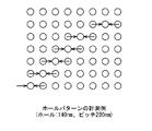
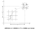
例えば、図1に示すようなホールパターンをArF露光装置で露光現像した場合、周辺から中心方向に向かって計測すると、周辺から数十μmにわたり、10nm以上徐々にホール寸法が大きく変化していく。その一方で、前記ホールパターンについて、光近接効果シミュレーションを行うと、最外周のパターンのみの寸法が2nm程度小さくなるだけである。即ち、実験による結果と光近接効果シミュレーションとの乖離が発生しおり、パターン寸法が距離や開口率により変動し、ローカルフレアによる影響が発生していることが判る。
【0018】
即ち、着目する任意の実デバイスパターン(実際にリソグラフィー工程で作製されるデバイスパターン)において、当該実デバイスパターンの周辺のパターンを探し出し、距離の関数で実デバイスパターンの開口率を算出する。前記関数は、より近接している場所の影響を強く表現できるものであることが必要であり、ガウシアン関数やダブルガウシアン関数、三角波の関数等が適当である。このとき、本発明では、処理速度の向上を考慮して、各実デバイスパターンを有する露光領域を複数の補正領域に分割し、補正領域ごとに開口率を算出する。具体的には、露光領域を一辺数μm程度のオーダーでメッシュの補正領域に区切り、そのメッシュ内で開口率は均一なものとして計算する。これは面積密度法と呼ばれており、処理速度を大幅に向上させることができる。
【0019】
実デバイスパターンの寸法変動を算出するには、光強度プロファイルをガウシアンもしくは台形の関数で近似し、パターンデータから算出した開口率と試料基板上に形成されたパターンのSEM等による実測寸法との相関を求める。これにより、任意パターンの周辺の開口率を関数で近似し、寸法変動を予測することができる。実デバイスパターンの設計データを補正することにより、光リソグラフィーにおけるローカルフレアの影響の補正されたパターンを備えたフォトマスク(レチクル)を作製することが可能となる。なお、レチクル寸法を補正する場合、光近効果があるため、前記寸法変動をレチクル寸法変化量に換算もしくは光近接効果補正処理を行い、所望のレチクル上の寸法データを作成する。
【0020】
−具体的な実施形態−
以下、上述した本発明の基本骨子を踏まえ、具体的な実施形態について説明する。
本実施形態では、リソグラフィー工程において形成するデバイスパターンの寸法を修正するパターン寸法補正装置及び補正方法を開示する。なお、本実施形態では、パターン寸法の変動が露光装置のローカルフレアによる影響とした場合を記述するが、エッチング工程におけるローディング効果による影響も同様に周辺のパターンの開口率との関係から導き出すことができる。
【0021】
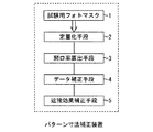
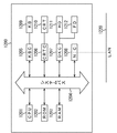
このパターン寸法補正装置は、図2に示すように、テストパターンを有する試験用フォトマスク1と、この試験用フォトマスク1を用いて、テストパターンにおける寸法変動を距離の関数として開口率との関係で定量化する定量化手段2と、複数の実デバイスパターンを有する露光領域を複数の補正領域に分割し、補正領域ごとに開口率を算出する開口率算出手段3と、開口率算出手段3で算出された開口率を試験用フォトマスク1を用いた定量化の結果に入力して、実デバイスパターンの寸法変動を補正領域ごとに算出し、これに基づき実デバイスパターンの設計データを補正するデータ補正手段4と、近接効果を補正する近接効果補正手段5とを含み構成されている。
【0022】
以下、上記構成のパターン寸法補正装置を用いた補正方法について、上述の各手段の機能と共に説明する。
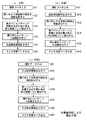
図3は、パターン寸法補正の各手順を示すフローチャートである。
図3(a)の手順1では、開口率とパターン寸法変動の関係に基づき、後述するステップS2〜5を経ることにより実デバイスパターンの寸法を各補正領域の開口率から補正を行い、その後、近接効果補正手段5を用いたステップS6による光近接効果補正を行って、作製するレチクル用の設計データを作成する。
【0023】
また、図3(b)の手順2では、ステップS12による光近接効果補正を行った後に、後述するステップS13〜16を経ることにより実デバイスパターンの寸法を各補正領域の開口率から補正を行い、作製するレチクル用の設計データを作成する。なお、前記補正値はウェーハ上の数値であるため、レチクル上の寸法補正値としては、露光条件やパターン種に応じた値をとることになる。手順1,2のように、光近接効果補正を付随的に行うのは、光近接効果補正と開口率変化に伴う寸法変動とは独立に発生するものであり、各々の補正を独立して行う必要があるためである。
【0024】
更に、図3(c)の手順3では、ステップS22による光近接効果補正を行った後に、後述するステップS23〜26を経て、再びステップS27による光近接効果補正を行って、作製するレチクル用の設計データを作成する。これは、例えば、光近接効果補正した後にパターン開口率による補正を行うと、補正された設計データ通りに試料基板上のフォトレジストにパターン形成を行うためには、再度の光近接効果補正が必要になる場合があるからである。
【0025】
以下、図3(a)を例に採り、ステップS1〜6を説明する。
始めに、設計データをパターン寸法補正装置に入力する(ステップS1)。
続いて、定量化手段2により、試験用フォトマスク1を用いて、テストパターンにおける寸法変動を距離の関数として開口率との関係で定量化する(ステップS2)。
【0026】
ここで、試験用フォトマスク1は、図4(a)に示すように、テストパターン21を有しており、各テストパターンは、例えばパターン寸法(ここではライン幅)が120μmの試験パターン11と、この試験パターン11を囲む輪帯形状の光透過領域を形成する例えば2.76μm幅のフレア発生パターン12とが組み合わされた基本構成を有して構成されている。ここでは、フレア発生パターン12の半径を変えて露光することで、計測する中心の試験パターン11に与える開口率と距離の関係を求めている。露光は、ArF露光装置でポジ型のレジストを用い、フレア発生パターン12の露光を行わない試験パターン11のみの露光を基準としている。
【0027】
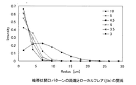
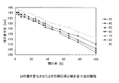
図4(b)に、フレア発生パターン12の露光の半径と試験パターン11に生じたパターン寸法変動との関係を示す。ここでは、パターン寸法変動を基準の基準の試験パターン11のみで露光した場合との差分で表している。
フレア発生パターン12の露光の半径が大きい領域では、遠くからのローカルフレアの影響を受けることになり、ある程度の距離が離れると寸法変動が発生せずに、基準の試験パターン11のみを形成した場合と同じ寸法が得られる(差分値が0に近い値となる。)。その一方で、フレア発生パターン12が近づくとローカルフレアの影響を受け、試験パターン11のパターン寸法の測定値(差分値)が大きくなることが判る。
【0028】
続いて、開口率算出手段3により、分割された補正領域ごとに開口率を算出する(ステップS3)。
ここで、任意の実デバイスパターンにおいて、ローカルフレアの影響を受ける開口率を計算するには、任意のパターン各々において、近接するパターンを距離の関数として積分することで算出できる。開口率を近似する関数としては、γを開口率の影響とした場合、式(1)に示すガウシアン関数や式(2)に示す三角波が利用可能である。
【0029】
【数1】

上述のように、任意の全てのパターンについて計算する場合、処理速度に著しい遅延を来すことになる。そこで本実施形態では、実用的な処理速度を得るため、複数の実デバイスパターンを有する露光領域を複数の補正領域に分割、ここでは任意のグリッドでメッシュ分割し、補正領域単位で開口率を求めている。このように補正領域に分割し、パターン密度を近似する方法は、電子線露光技術において、後方散乱電子の影響を計算する際、面積密度法と呼ばれている(特開2001−52999)。分割した補正領域で、パターン開口率を表現する場合、分割するグリッドの大きさは、ローカルフレア等の影響を及ぼす範囲の1/10程度以下にすることが望ましい。
【0031】
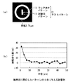
例えば、図4(a)に示したようなテストパターンを基に、(1)式で示すガウシアン関数でローカルフレアの影響(γ)を計算した結果を図5に示す。
図4(b)の実験結果と図5の計算結果とを比較すると、γ値は5μm程度であり、分布の傾向が一致することが判る。即ち、開口率の影響は5μm程度とし、0.5μm程度のグリッドで分割して補正領域を形成するのが妥当と考えられる。
【0032】
ここで、開口率を近似する関数としては、(1)式で示すガウシアン関数(シングルガウシアン関数)に替わり、2つのガウシアン関数(ダブルガウシアン関数)、或いは3つ以上のガウシアン関数を用いることも考えられる。そこで、ダブルガウシアン関数を例に採り、その適用の可否について考察する。
【0033】
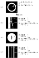
ローカルフレア発生のテストパターンとしては、図4(a)の例のみならず、例えば図6(a)〜図6(d)のような4種のものを用いることも考えられる。図6(a)は輪帯形状の光透過領域を形成する例えば2.7μm幅のフレア発生パターン31のみを有するテストパターン22、図6(b)は帯状のフレア発生パターン33及びこのフレア発生パターン33と順次離間されてなる複数のライン状の試験用パターン32を有するテストパターン23、図6(c)は円盤状にくり貫かれたフレア発生パターン35及びこのフレア発生パターン35内に配されたライン状の遮光パターン34を有するテストパターン24、図6(d)は帯状の試験用パターン36及びこれと平行に形成された帯状(幅1μm)のフレア発生パターン37を有するテストパターン25を例示している。
【0034】
任意のパターンに影響を与える開口率を任意のパターンからの距離の関数として算出する場合、図6(a)〜図6(d)のような4種類パターンで推測することも可能であり、同一の解が導き出せるはずである。
【0035】
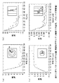
開口率の影響をシングルガウシアン関数でフィッティングした結果を図7に示す。ここで、図6(a)のテストパターンの場合が図7(a)に対応し、図6(b)が図7(b)、図6(c)が図7(c)、図6(d)が図7(d)にそれぞれ対応する。テストパターンによって、フィッティングのされ方が異なっているのが判る。傾向としては、より遠くの影響を受けている一方、任意パターン近傍で寸法が変化しているところがあることが判る。つまり、実験結果をより忠実に表現しようとした場合、複数のガウシアン関数でより精度良く合わせ込める可能性がある。
【0036】
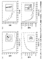
そこで、開口率の影響を2つのガウシアン関数、即ち、下記のダブルガウシアン関数(1’)式でフィッティングした結果を図8に示す。なお、βは、開口率の影響を寸法変動に取り込む際の係数である。図8でも図7と同様に、図6(a)のテストパターンの場合が図8(a)に対応し、図6(b)が図8(b)、図6(c)が図8(c)、図6(d)が図8(d)にそれぞれ対応する。
【0037】
【数2】
このように、シングルガウシアン関数よりもダブルガウシアン関数を用いた方が、4つのテストパターン全てに精度良く合わせ込めていることが判る。
【0039】
図9を参照して、面積密度法による、ローカルフレアの影響に基づいた実効的な面積密度をガウシアン近似により計算する方法を説明する。図9は、露光データを寸法がA×Aの矩形形状の補正領域に分割した状態を示す図である。ここで、(lA, mA)だけ離れた( i + l, j + m)番目の補正領域の寸法変動量は露光装置によるローカルフレア等に起因する拡がりを有するので、( i, j)番目の補正領域の寸法変動に影響を与える。この(lA, mA)だけ離れた( i + l, j + m)番目の補正領域からのローカルフレアによる寄与al,mはA×Aの領域からの影響を積分する形で以下の式(3)により表すことができる。三角波で近似する場合は、式(3)のexp部を式(2)に置き換えればよい。
【0040】
【数3】
ここで、(lA, mA)だけ離れた( i + l, j + m)番目の補正領域におけるパターンの面積密度をαi+l, j+mとすると、( i + l, j + m)番目の補正領域からのローカルフレアの寄与分は、al,m×αi+l, j+mとなる。従って平滑化処理後の( i,j)番目の補正領域の実効的な面積密度α’i, jを中心とする半径2γ程度の領域にある各補正領域からの寄与を総和として取り込めば良く、式(4)で表すことができる。
【0042】
【数4】
続いて、データ補正手段4により、算出された開口率とパターン寸法変動との関係を関数で示す(ステップS4)。
近似の手法としては、ガウシアンの関数もしくは台形波形が利用できる。例えば、ガウシアン関数で寸法変動値を近似した場合、寸法変動に関係するパラメータをαとすると式(5)で表すことができる。
【0044】
【数5】
即ち、任意のパターンにおける寸法は、開口率を取り込んだ式(4)と寸法変動を説明する式(5)を面積分した値の和に関係してくる。補正後のパターン寸法をWとすると、式(6)に示すように、上記開口率分と寸法変動分の和が、ある閾値(Threshold)となる値から算出できる。なお、βは、開口率の影響を寸法変動に取り込む際の係数である。
【0046】
【数6】
このように、ダブルガウシアンでパターン寸法の補正値を算出する場合、寸法変動量を第1項で示すガウシアンで十分説明できるかが問題となる。そこで、上記ダブルガウシアンを用い、求めた任意のパターンにおける開口率と寸法変動を推測した例を示す。(3)式及び(5)式で必用となるα、β、γのパラメータを図4(b)に示す開口率とパターン寸法との関係に近似させる際に、α値を意図的に変化させてフィッティングし、パターン寸法が140nmのパターンについてシミュレーションした結果を図10に示す。αの値が80nmより大きくなると、αが70nm以下の集団から寸法補正値が乖離し始める。これは、任意のパターンサイズにおいて、開口率をパターン寸法に表現するうえで有効なαの値が存在していることを示しており、αは対象とするパターンサイズの1/2以下にする必用があることが判る。
【0048】
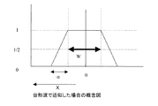
このことは、開口率とパターン寸法との関係がリニアに近く変動しており、ガウシアンでは、裾やピーク付近では、リニア関数から急激にずれることに起因していると推測される。そこで、図11に示すように、近似の関数として台形波を用いることも可能なことが判る。台形波で近似する場合には、式(6)の第1項を式(7)で表現できる。開口率が0〜100%まで最大に変化したときの寸法差をα、任意強度が1/2で寸法Wになっている。
0≦ x < w/2 − α/2 の場合 f(x) = 1
w/2 − α/2 ≦ x ≦ w/2 + α/2 の場合 f(x) = 0.5(x − w/2)/ α − 1/2x > w/2 + α/2 の場合 f(x) = 0・・・(7)
【0049】
このようにして、任意の実デバイスパターンにおける開口率を補正領域毎にガウシアンもしくは三角波で近似し、パターン寸法の変動量を開口率に関係して補正できるようにガウシアンもしくは台形波で近似し、補正量を抽出・補正する手順となる。なお参考として、電子線リソグラフィー技術では、物理的な意味をもった前方散乱および後方散乱を各々ガウシアンで近似し、補正領域毎に近接効果補正を行う手法がある(特開2001−112787、特開2001−153233)。
【0050】
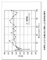
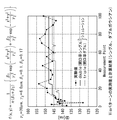
任意のパターン寸法を、開口率の影響を面積密度法に基づきガウシアン関数で近似し、寸法変化量をガウシアン関数で近似した場合の評価結果を図12に示す。
この計算において、パラメータα、β、γは、図4(b)に示す露光結果よりフィッティングした。実測値は、ArF露光装置、ポジ型レジストを使用し、SEMで実測した値である。なお、評価は図1に示すホールパターン(ピッチ280nm、Via140nmのパターンが並んでいるパターン)で行われており、パターン領域のコーナーから中心に向かって、SEMによる実測及び計算を行っている。横軸は、パターン領域のコーナーから中心に向かって計測された数であり、縦軸は実測及び計算したホール寸法である。ホール寸法は、中心に向かって寸法が大きくなっているが、本実施形態の方法により計算した値で説明できることが判る。この場合には、パターン寸法の変動量をガウシアンで近似した結果であるが、台形波でも同様な結果が得られている。即ち、本実施形態により、ローカルフレアの影響に起因する寸法変動が開口率により変化することを説明でき、この値に基づいてパターン寸法値の補正を行うことで、高精度の寸法精度が得られることが判る。
【0051】
更に、任意のパターン寸法を、開口率の影響を面積密度法に基づきダブルガウシアン関数で近似し、寸法変化量をガウシアン関数で近似した場合の評価結果を図12に加えた様子を図13に示す。
このように、開口率の影響をダブルガウシアン関数で近似した場合も、これをシングルダブルガウシアン関数で近似した場合と同様、ローカルフレアの影響に起因する寸法変動が開口率により変化することを説明でき、この値に基づいてパターン寸法値の補正を行うことで、高精度の寸法精度が得られることが判る。
【0052】
なお、本実施形態では、開口率変動に伴う寸法補正について述べたが、上述したように光リソグラフィーでは光近接効果の影響があるため、この開口率による寸法補正を行った後、光近接効果補正を加える(ステップS5)。因みに、本実施形態における試験用フォトマスク1の試験用パターン21では、光近接効果補正量は、最外周パターンのみ2nm程マスクサイズを大きくすることになる。
【0053】
そして、レチクルを作製するための実デバイスパターンの設計データを出力する(ステップS6)。
【0054】
なお、本実施形態では、露光即ちローカルフレアによる影響の補正について述べたが、開口率に関係して寸法変動するエッチングにおけるローディング効果の補正も同様に行うことが可能である。
【0055】
以上説明したように、本実施形態によれば、光リソグラフィーにおいて露光されるパターンに発生する寸法変動を定量的に見積もり、これに基づいてパターン寸法を容易且つ正確に補正し、極めて信頼性の高いデバイスを製造することが可能となる。
【0056】
上述した実施形態によるパターン寸法補正装置及び方法を構成する各手段、並びにターン寸法補正方法の各ステップ(図3(a)のステップ1〜6、図3(b)のステップ11〜16、図3(c)のステップ21〜27)は、コンピュータのRAMやROMなどに記憶されたプログラムが動作することによって実現できる。このプログラム及び当該プログラムを記録したコンピュータ読み取り可能な記憶媒体は本発明に含まれる。
【0057】
具体的に、前記プログラムは、例えばCD−ROMのような記録媒体に記録し、或いは各種伝送媒体を介し、コンピュータに提供される。前記プログラムを記録する記録媒体としては、CD−ROM以外に、フレキシブルディスク、ハードディスク、磁気テープ、光磁気ディスク、不揮発性メモリカード等を用いることができる。他方、前記プログラムの伝送媒体としては、プログラム情報を搬送波として伝搬させて供給するためのコンピュータネットワーク(LAN、インターネットの等のWAN、無線通信ネットワーク等)システムにおける通信媒体(光ファイバ等の有線回線や無線回線等)を用いることができる。
【0058】
また、コンピュータが供給されたプログラムを実行することにより上述の実施形態の機能が実現されるだけでなく、そのプログラムがコンピュータにおいて稼働しているOS(オペレーティングシステム)或いは他のアプリケーションソフト等と共同して上述の実施形態の機能が実現される場合や、供給されたプログラムの処理の全て或いは一部がコンピュータの機能拡張ボードや機能拡張ユニットにより行われて上述の実施形態の機能が実現される場合も、かかるプログラムは本発明に含まれる。
【0059】
例えば、図14は、一般的なパーソナルユーザ端末装置の内部構成を示す模式図である。この図14において、1200はコンピュータPCである。PC1200は、CPU1201を備え、ROM1202又はハードディスク(HD)1211に記憶された、或いはフレキシブルディスクドライブ(FD)1212より供給されるデバイス制御ソフトウェアを実行し、システムバス1204に接続される各デバイスを総括的に制御する。
【0060】
以下、本発明の諸態様を付記としてまとめて記載する。
【0061】
(付記1)フォトリソグラフィーにおいて形成する実デバイスパターンに、その周辺に存する光透過領域の開口率に依存して発生する寸法変動を補正するパターン寸法補正装置であって、
テストパターンを有する試験用フォトマスクと、
前記試験用フォトマスクを用いて、前記テストパターンにおける前記寸法変動を距離の関数として前記開口率との関係で定量化する定量化手段と、
複数の前記実デバイスパターンを有する露光領域を複数の補正領域に分割し、前記補正領域ごとに前記開口率を算出する開口率算出手段と、
前記開口率算出手段で算出された前記開口率を前記定量化の結果に入力して、前記実デバイスパターンの前記寸法変動を前記補正領域ごとに算出し、これに基づき前記実デバイスパターンの設計データを補正するデータ補正手段と
を含むことを特徴とするパターン寸法補正装置。
【0062】
(付記2)前記試験用フォトマスクの前記テストパターンは、前記寸法変動を見積もる対象となる測定用パターンと、前記測定用パターンに前記寸法変動を発生せしめる光透過領域であり、前記測定用パターンからの距離の異なる複数のフレア発生パターンとを有することを特徴とする付記1に記載のパターン寸法補正装置。
【0063】
(付記3)前記定量化手段は、前記各フレア発生パターンに対応した前記測定用パターンの前記寸法を、当該測定用パターンと前記各フレア発生パターンとの前記距離との関係で定量化し、これに基づき前記寸法変動を前記開口率との関係で定量化することを特徴とする付記2に記載のパターン寸法補正装置。
【0064】
(付記4)前記開口率算出手段は、前記各補正領域の面積密度を求め、ガウシアン関数を用いた近似計算により前記開口率を算出することを特徴とする付記1〜3のいずれか1項に記載のパターン寸法補正装置。
【0065】
(付記5)前記開口率算出手段は、前記各補正領域の面積密度を求め、少なくとも2つのガウシアン関数を用いた近似計算により前記開口率を算出することを特徴とする付記1〜3のいずれか1項に記載のパターン寸法補正装置。
【0066】
(付記6)前記データ補正手段は、前記開口率の変動による前記実デバイスパターンの前記寸法変動を、ガウシアン関数を用いた近似計算により算出することを特徴とする付記1〜5のいずれか1項に記載のパターン寸法補正装置。
【0067】
(付記7)前記データ補正手段による前記寸法変動の算出に用いるガウシアン関数は、ガウシアンの1/eの値が前記実デバイスパターンに含まれる最小パターン幅の1/2以下であり、且つ1/2に近い数値であることを特徴とする付記6に記載のパターン寸法補正装置。
【0068】
(付記8)前記データ補正手段は、前記開口率の変動による前記実デバイスパターンの前記寸法変動を、台形関数を用いた近似計算により算出することを特徴とする付記1〜5のいずれか1項に記載のパターン寸法補正装置。
【0069】
(付記9)光近接効果補正手段を更に含むことを特徴とする付記1〜8のいずれか1項に記載のパターン寸法補正装置。
【0070】
(付記10)複数の実デバイスパターンを有する露光領域を複数の補正領域に分割し、前記補正領域ごとにその光透過領域の開口率を算出する開口率算出手段と、
算出された前記開口率を用い、前記実デバイスパターンに発生する寸法変動を前記補正領域ごとに算出し、これに基づき前記実デバイスパターンの設計データを補正するデータ補正手段と
を含むことを特徴とするパターン寸法補正装置。
【0071】
(付記11)前記開口率算出手段は、前記各補正領域の面積密度を求め、ガウシアン関数を用いた近似計算により前記開口率を算出することを特徴とする付記10に記載のパターン寸法補正装置。
【0072】
(付記12)前記開口率算出手段は、前記各補正領域の面積密度を求め、少なくとも2つのガウシアン関数を用いた近似計算により前記開口率を算出することを特徴とする付記10に記載のパターン寸法補正装置。
【0073】
(付記13)前記データ補正手段は、前記開口率の変動による前記実デバイスパターンの前記寸法変動を、ガウシアン関数を用いた近似計算により算出することを特徴とする付記10〜12のいずれか1項に記載のパターン寸法補正装置。
【0074】
(付記14)前記データ補正手段による前記寸法変動の算出に用いるガウシアン関数は、ガウシアンの1/eの値が前記実デバイスパターンに含まれる最小パターン幅の1/2以下であり、且つ1/2に近い数値であることを特徴とする付記13に記載のパターン寸法補正装置。
【0075】
(付記15)前記データ補正手段は、前記開口率の変動による前記実デバイスパターンの前記寸法変動を、台形関数を用いた近似計算により算出することを特徴とする付記10〜12のいずれか1項に記載のパターン寸法補正装置。
【0076】
(付記16)光近接効果補正手段を更に含むことを特徴とする付記10〜15のいずれか1項に記載のパターン寸法補正装置。
【0077】
(付記17)フォトリソグラフィーにおいて形成する実デバイスパターンに、その周辺に存する光透過領域の開口率に依存して発生する寸法変動を補正するパターン寸法補正方法であって、
テストパターンを有する試験用フォトマスクを用いて、前記テストパターンにおける前記寸法変動を距離の関数として前記開口率との関係で定量化する第1のステップと、
複数の前記実デバイスパターンを有する露光領域を複数の補正領域に分割し、前記補正領域ごとに前記開口率を算出する第2のステップと、
算出された前記開口率を前記定量化の結果に入力して、前記実デバイスパターンの前記寸法変動を前記補正領域ごとに算出し、これに基づき前記実デバイスパターンの設計データを補正する第3のステップと
を含むことを特徴とするパターン寸法補正方法。
【0078】
(付記18)前記試験用フォトマスクの前記テストパターンは、前記寸法変動を見積もる対象となる測定用パターンと、前記測定用パターンに前記寸法変動を発生せしめる光透過領域であり、前記測定用パターンからの距離の異なる複数のフレア発生パターンとを有することを特徴とする付記17に記載のパターン寸法補正方法。
【0079】
(付記19)前記第1のステップは、前記各フレア発生パターンに対応した前記測定用パターンの前記寸法を、当該測定用パターンと前記各フレア発生パターンとの前記距離との関係で定量化し、これに基づき前記寸法変動を前記開口率との関係で定量化することを特徴とする付記18に記載のパターン寸法補正方法。
【0080】
(付記20)前記第2のステップは、前記各補正領域の面積密度を求め、ガウシアン関数を用いた近似計算により前記開口率を算出することを特徴とする付記17〜19のいずれか1項に記載のパターン寸法補正方法。
【0081】
(付記21)前記第2のステップは、前記各補正領域の面積密度を求め、少なくとも2つのガウシアン関数を用いた近似計算により前記開口率を算出することを特徴とする付記17〜19のいずれか1項に記載のパターン寸法補正方法。
【0082】
(付記22)前記第3のステップは、前記開口率の変動による前記実デバイスパターンの前記寸法変動を、ガウシアン関数を用いた近似計算により算出することを特徴とする付記17〜21のいずれか1項に記載のパターン寸法補正方法。
【0083】
(付記23)前記第3のステップによる前記寸法変動の算出に用いるガウシアン関数は、ガウシアンの1/eの値が前記実デバイスパターンに含まれる最小パターン幅の1/2以下であり、且つ1/2に近い数値であることを特徴とする付記22に記載のパターン寸法補正方法。
【0084】
(付記24)前記第3のステップは、前記開口率の変動による前記実デバイスパターンの前記寸法変動を、台形関数を用いた近似計算により算出することを特徴とする付記17〜21のいずれか1項に記載のパターン寸法補正方法。
【0085】
(付記25)光近接効果の補正手段を行う第4のステップを更に含むことを特徴とする付記17〜24のいずれか1項に記載のパターン寸法補正方法。
【0086】
(付記26)前記第4のステップは、前記第1のステップの前又は前記第3のステップの後、或いは前記第1のステップの前及び前記第3のステップの後の双方に実行されることを特徴とする付記25に記載のパターン寸法補正方法。
【0087】
(付記27)複数の実デバイスパターンを有する露光領域を複数の補正領域に分割し、前記補正領域ごとにその光透過領域の開口率を算出する第1のステップと、
算出された前記開口率を用い、前記実デバイスパターンに発生する寸法変動を前記補正領域ごとに算出し、これに基づき前記実デバイスパターンの設計データを補正する第2のステップと
を含むことを特徴とするパターン寸法補正方法。
【0088】
(付記28)前記第1のステップは、前記各補正領域の面積密度を求め、ガウシアン関数を用いた近似計算により前記開口率を算出することを特徴とする付記27に記載のパターン寸法補正方法。
【0089】
(付記29)前記第1のステップは、前記各補正領域の面積密度を求め、少なくとも2つのガウシアン関数を用いた近似計算により前記開口率を算出することを特徴とする付記27に記載のパターン寸法補正方法。
【0090】
(付記30)前記第2のステップは、前記開口率の変動による前記実デバイスパターンの前記寸法変動を、ガウシアン関数を用いた近似計算により算出することを特徴とする付記27〜29のいずれか1項に記載のパターン寸法補正方法。
【0091】
(付記31)前記第2のステップによる前記寸法変動の算出に用いるガウシアン関数は、ガウシアンの1/eの値が前記実デバイスパターンに含まれる最小パターン幅の1/2以下であり、且つ1/2に近い数値であることを特徴とする付記30に記載のパターン寸法補正方法。
【0092】
(付記32)前記第2のステップは、前記開口率の変動による前記実デバイスパターンの前記寸法変動を、台形関数を用いた近似計算により算出することを特徴とする付記27〜29のいずれか1項に記載のパターン寸法補正方法。
【0093】
(付記33)光近接効果の補正手段を行う第3のステップを更に含むことを特徴とする付記27〜32のいずれか1項に記載のパターン寸法補正方法。
【0094】
(付記34)前記第3のステップは、前記第1のステップの前又は前記第2のステップの後、或いは前記第1のステップの前及び前記第2のステップの後の双方に実行されることを特徴とする付記33に記載のパターン寸法補正方法。
【0095】
(付記35)フォトリソグラフィーにおいて形成する実デバイスパターンに、その周辺に存する光透過領域の開口率に依存して発生する寸法変動を補正するに際して、
テストパターンを有する試験用フォトマスクを用いて、前記テストパターンにおける前記寸法変動を距離の関数として前記開口率との関係で定量化する第1のステップと、
複数の前記実デバイスパターンを有する露光領域を複数の補正領域に分割し、前記補正領域ごとに前記開口率を算出する第2のステップと、
算出された前記開口率を前記定量化の結果に入力して、前記実デバイスパターンの前記寸法変動を前記補正領域ごとに算出し、これに基づき前記実デバイスパターンの設計データを補正する第3のステップと
をコンピュータに実行させるためのプログラム。
【0096】
(付記36)付記35に記載のプログラムを記録したことを特徴とするコンピュータ読み取り可能な記録媒体。
【0097】
(付記37)複数の実デバイスパターンを有する露光領域を複数の補正領域に分割し、前記補正領域ごとにその光透過領域の開口率を算出する第1のステップと、
算出された前記開口率を用い、前記実デバイスパターンに発生する寸法変動を前記補正領域ごとに算出し、これに基づき前記実デバイスパターンの設計データを補正する第2のステップと
をコンピュータに実行させるためのプログラム。
【0098】
(付記38)付記37に記載のプログラムを記録したことを特徴とするコンピュータ読み取り可能な記録媒体。
【0099】
【発明の効果】
本発明によれば、リソグラフィーにおいて露光されるパターンに発生する寸法変動を定量的に見積もり、これに基づいてパターン寸法を容易且つ正確に補正し、極めて信頼性の高いデバイスを製造することを可能とするパターン寸法補正装置及び補正方法を提供することができる。
【図面の簡単な説明】
【図1】ホールパターンをArF露光装置で露光現像した場合の様子を示す概略平面図である。
【図2】本実施形態のパターン寸法補正装置の概略構成を示すブロック図である。
【図3】本実施形態のパターン寸法補正の各手順を示すフローチャートである。
【図4】試験用フォトマスクの概略構成及び輪帯パターンの露光の半径と試験パターンに生じたパターン寸法変動との関係を示す模式図である。
【図5】図4に示したようなテストパターンを基に、ガウシアン関数でローカルフレアの影響を計算した結果を示す特性図である。
【図6】ローカルフレア発生のテストパターンの他の例を示す模式図である。
【図7】開口率の影響をシングルガウシアン関数でフィッティングした結果を示す特性図である。
【図8】開口率の影響をダブルガウシアン関数でフィッティングした結果を示す特性図である。
【図9】面積密度法による、ローカルフレアの影響に基づいた実効的な面積密度をガウシアン近似による計算方法を説明するための模式図である。
【図10】α、β、γのパラメータを開口率とパターン寸法との関係に近似させる際に、α値を意図的に変化させてフィッティングし、パターン寸法が140nmのパターンについてシミュレーションした結果を示す特性図である。
【図11】近似の関数として台形波を用いる場合を示す特性図である。
【図12】任意のパターン寸法を、開口率の影響を面積密度法に基づきガウシアン関数で近似し、寸法変化量をガウシアンで近似した場合の評価結果を示す特性図である。
【図13】任意のパターン寸法を、開口率の影響を面積密度法に基づきダブルガウシアン関数で近似し、寸法変化量をガウシアンで近似した場合の評価結果を図12に付加して示す特性図である。
【図14】一般的なパーソナルユーザ端末装置の内部構成を示す模式図である。
【符号の説明】
1 試験用フォトマスク
2 定量化手段
3 開口率算出手段
4 データ補正手段
5 近接効果補正手段
11,32,34,36 試験用パターン
12,31,33,35,37 フレア発生パターン
21,22,23,24,25 テストパターン[0001]
TECHNICAL FIELD OF THE INVENTION
The present invention relates to a pattern dimension correction apparatus and a correction method for correcting the dimensions of a device pattern formed in a lithography step, which is one of the manufacturing steps of a semiconductor device, for example, a semiconductor chip such as an IC or LSI, or a display element such as a liquid crystal panel. It is suitable for application to the manufacture of various devices such as a detection element such as a magnetic head and an imaging element such as a CCD.
[0002]
[Prior art]
2. Description of the Related Art In a pattern forming technique, a semiconductor device is manufactured using optical lithography. Optical lithography is a technique in which a desired pattern is formed on a reticle, which is a photomask, and the pattern is transferred onto a sample substrate via a reduction optical system. A photosensitive resin called a resist is formed on the sample substrate, and the latent image of the transferred pattern is etched by forming a pattern using the difference in the dissolution rate between the exposed and unexposed parts by the developer. Thereby, desired material processing can be performed.
[0003]
In the exposure technique, in order to transfer a fine pattern with high precision, the wavelength of exposure light, the reticle structure are optimized, and in addition, the influence of a nearby pattern is calculated and calculated for correction. This correction is called OPC (Optical Proximity Correction), and calculates the influence of the optical proximity effect on the transferred image of the pattern by taking into account the illumination conditions (NA, Sigma) and exposure conditions (resist material, exposure wavelength) of the exposure apparatus. A correction amount is calculated by an experiment to correct the reticle size.
[0004]
However, there is a component that cannot be corrected by the OPC, for example, a dimensional difference of a dense / dense pattern due to a flare of an exposure apparatus or etching, and the size of a formed pattern varies. Flare of the exposure apparatus is caused by minute unevenness of the lens, fluctuation of the refractive index, and reflected and scattered light on the wafer surface. Furthermore, recently, the occurrence of local flare depending on the situation around each pattern has been regarded as a problem. This is so-called local flare, which is caused by the specificity of the lens material depending on the wavelength of the exposure light to be used (short wavelength represented by 193 nm) and the like. It is the main cause of unexpected changes. In addition, in the etching, in a region having a large area to be etched, a lack of a reaction gas or an increase in a reaction product occurs, and the pattern formation accuracy is deteriorated due to the area dependency and the size dependency in an arbitrary region.
[0005]
[Patent Document 1]
JP 2001-52999 A
[Patent Document 2]
JP 2001-112787 A
[Patent Document 3]
JP 2001-153233 A
[Non-patent document 1]
Tae Moon Jong, and soon (Samsung), 'Flare in Microlithographic Exposure Tools', Jpn. J. Appl. Phys. Vol. 41 (2002) 5113.
[0006]
[Problems to be solved by the invention]
However, it is difficult to accurately correct a dimensional change due to a local flare of the exposure apparatus or a loading effect in etching.
[0007]
The local flare described above must be quantified and removed in order to form a desired pattern in a semiconductor device in a favorable manner. Therefore, at present, there is no suitable method for consciously solving this problem by specifically identifying this local flare.
[0008]
In the case of the optical proximity effect correction, the optical proximity effect is calculated from a pattern in a region of several μm. However, it is difficult to calculate the optical proximity effect to a range of several tens of μm due to flare due to time constraints. Yes, and it was difficult to explain by the proximity effect of light intensity. In addition, the effect of the loading effect on the etching cannot be naturally explained by the light intensity calculation.
[0009]
The present invention has been made to solve the above problem, and quantitatively estimates a dimensional variation occurring in a pattern to be exposed in lithography, and easily and accurately corrects a pattern dimension based on the quantitative variation to achieve extremely high reliability. It is an object of the present invention to provide a pattern dimension correction apparatus and a correction method that can manufacture a device having high accuracy.
[0010]
[Means for Solving the Problems]
As a result of intensive studies, the present inventor has reached various aspects of the invention described below.
[0011]
A pattern dimension correcting apparatus and a pattern correcting method according to the present invention are intended to correct a dimensional change that occurs in an actual device pattern formed in photolithography depending on an aperture ratio of a light transmitting region around the actual device pattern.
[0012]
The pattern dimension correcting apparatus of the present invention uses a test photomask having a test pattern and the test photomask to quantify the dimensional variation in the test pattern as a function of distance in relation to the aperture ratio. Quantification means, an exposure area having a plurality of the actual device patterns, divided into a plurality of correction areas, and an aperture ratio calculation means for calculating the aperture ratio for each of the correction areas; Data correction means for inputting the aperture ratio into the result of the quantification, calculating the dimensional variation of the actual device pattern for each of the correction regions, and correcting the design data of the actual device pattern based on the calculated data. .
[0013]
Another aspect of the pattern dimension correcting apparatus of the present invention is an aperture ratio calculating unit that divides an exposure region having a plurality of actual device patterns into a plurality of correction regions, and calculates an aperture ratio of a light transmission region for each of the correction regions. And a data correction means for calculating a dimensional change occurring in the real device pattern for each correction area using the calculated aperture ratio, and correcting design data of the real device pattern based on the calculated dimensional change.
[0014]
The pattern dimension correcting method according to the present invention includes a first step of quantifying the dimension variation in the test pattern as a function of a distance in relation to the aperture ratio using a test photomask having a test pattern; Dividing the exposure area having the actual device pattern into a plurality of correction areas, calculating the aperture ratio for each correction area, and inputting the calculated aperture ratio to the result of the quantification. Calculating the dimensional variation of the actual device pattern for each of the correction areas, and correcting the design data of the actual device pattern based on the third step.
[0015]
Another aspect of the pattern dimension correction method of the present invention is a first step of dividing an exposure region having a plurality of actual device patterns into a plurality of correction regions and calculating an aperture ratio of a light transmission region for each of the correction regions. And a second step of calculating a dimensional change occurring in the actual device pattern for each correction area using the calculated aperture ratio, and correcting the design data of the actual device pattern based on the calculated dimension variation.
[0016]
BEST MODE FOR CARRYING OUT THE INVENTION
-Basic gist of the present invention-
First, the basic gist of the present invention will be described.
The present inventors have found that the influence of the loading effect on local flare or etching that causes dimensional variation in a pattern occurs in relation to the aperture ratio of a pattern close to a pattern of interest and the distance between the patterns.
[0017]
For example, when a hole pattern as shown in FIG. 1 is exposed and developed by an ArF exposure apparatus, when measured from the periphery toward the center, the hole size gradually changes by 10 nm or more over several tens μm from the periphery. On the other hand, when the light proximity effect simulation is performed on the hole pattern, only the dimension of the outermost pattern is reduced by about 2 nm. That is, it is understood that a difference between the result of the experiment and the simulation of the optical proximity effect has occurred, and that the pattern dimension varies with the distance and the aperture ratio, and that the influence of local flare has occurred.
[0018]
That is, in an arbitrary actual device pattern of interest (a device pattern actually produced in a lithography process), a pattern around the actual device pattern is searched for, and the aperture ratio of the actual device pattern is calculated as a function of distance. The function needs to be able to strongly express the influence of a closer place, and a Gaussian function, a double Gaussian function, a triangular wave function, or the like is appropriate. At this time, in the present invention, the exposure area having each actual device pattern is divided into a plurality of correction areas, and the aperture ratio is calculated for each correction area in consideration of an improvement in processing speed. Specifically, the exposure area is divided into mesh correction areas on the order of several μm on each side, and the calculation is performed assuming that the aperture ratio is uniform within the mesh. This is called an area density method, and can greatly improve the processing speed.
[0019]
To calculate the dimensional variation of the actual device pattern, the light intensity profile is approximated by a Gaussian or trapezoidal function, and the correlation between the aperture ratio calculated from the pattern data and the actual dimension of the pattern formed on the sample substrate measured by SEM or the like. Ask for. Thus, the aperture ratio around the arbitrary pattern can be approximated by the function, and the dimensional change can be predicted. By correcting the design data of the actual device pattern, a photomask (reticle) having a pattern in which the influence of local flare in optical lithography has been corrected can be manufactured. When the reticle size is corrected, since there is an optical proximity effect, the dimensional change is converted into a reticle dimensional change amount or an optical proximity effect correction process is performed to create desired reticle dimension data.
[0020]
-Specific embodiment-
Hereinafter, specific embodiments will be described based on the basic gist of the present invention described above.
In the present embodiment, a pattern dimension correction apparatus and a correction method for correcting a dimension of a device pattern formed in a lithography process are disclosed. In the present embodiment, a case is described in which the variation in the pattern dimension is caused by the local flare of the exposure apparatus. However, the effect of the loading effect in the etching process can be similarly derived from the relationship with the aperture ratio of the peripheral pattern. it can.
[0021]
As shown in FIG. 2, this pattern dimension correcting apparatus uses a
[0022]
Hereinafter, a correction method using the pattern dimension correction device having the above configuration will be described together with the functions of the above-described units.
FIG. 3 is a flowchart showing each procedure of the pattern dimension correction.
In the
[0023]
In the
[0024]
Further, in the
[0025]
Hereinafter, steps S1 to S6 will be described with reference to FIG.
First, design data is input to the pattern dimension correcting device (step S1).
Subsequently, the
[0026]
Here, as shown in FIG. 4A, the
[0027]
FIG. 4B shows the relationship between the radius of exposure of the
In the region where the radius of exposure of the
[0028]
Subsequently, the aperture ratio is calculated by the aperture ratio calculation means 3 for each of the divided correction regions (step S3).
Here, in an arbitrary actual device pattern, the aperture ratio affected by local flare can be calculated by integrating an adjacent pattern as a function of distance in each arbitrary pattern. As a function for approximating the aperture ratio, when γ is the effect of the aperture ratio, a Gaussian function represented by Expression (1) or a triangular wave represented by Expression (2) can be used.
[0029]
(Equation 1)
As described above, when calculating for any arbitrary pattern, there is a significant delay in processing speed. Therefore, in the present embodiment, in order to obtain a practical processing speed, the exposure region having a plurality of actual device patterns is divided into a plurality of correction regions, here, mesh division is performed using an arbitrary grid, and the aperture ratio is obtained in units of the correction region. ing. Such a method of dividing into correction regions and approximating the pattern density is called an area density method when calculating the influence of backscattered electrons in the electron beam exposure technique (Japanese Patent Application Laid-Open No. 2001-52999). When expressing the pattern aperture ratio in the divided correction area, it is desirable that the size of the divided grid is set to be about 1/10 or less of the range where local flare or the like affects.
[0031]
For example, FIG. 5 shows the result of calculating the influence (γ) of local flare by the Gaussian function shown in the equation (1) based on the test pattern shown in FIG.
Comparing the experimental result of FIG. 4B with the calculation result of FIG. 5, it can be seen that the γ value is about 5 μm, and the tendency of the distribution coincides. That is, it is considered appropriate that the effect of the aperture ratio is about 5 μm and the correction area is formed by dividing the grid by a grid of about 0.5 μm.
[0032]
Here, as a function for approximating the aperture ratio, two Gaussian functions (double Gaussian function) or three or more Gaussian functions may be used instead of the Gaussian function (single Gaussian function) shown in equation (1). Can be Thus, taking the double Gaussian function as an example, the applicability of the function is considered.
[0033]
As the test pattern for the occurrence of local flare, not only the example of FIG. 4A but also the use of, for example, four types as shown in FIGS. 6A to 6D can be considered. FIG. 6A shows a
[0034]
When calculating the aperture ratio affecting an arbitrary pattern as a function of the distance from the arbitrary pattern, it is possible to infer with four types of patterns as shown in FIGS. The solution of can be derived.
[0035]
FIG. 7 shows the result of fitting the effect of the aperture ratio with a single Gaussian function. Here, the case of the test pattern of FIG. 6A corresponds to FIG. 7A, FIG. 6B is FIG. 7B, FIG. 6C is FIG. 7C, FIG. FIG. 7D corresponds to FIG. It can be seen that the fitting is different depending on the test pattern. It can be seen that the tendency is that the dimension is changed near an arbitrary pattern while being affected by a greater distance. In other words, when trying to express the experimental result more faithfully, there is a possibility that a plurality of Gaussian functions can be used for more accurate matching.
[0036]
FIG. 8 shows the result of fitting the effect of the aperture ratio with two Gaussian functions, that is, the following double Gaussian function (1 ′). Here, β is a coefficient when the influence of the aperture ratio is taken into dimensional variation. 8, similarly to FIG. 7, the test pattern of FIG. 6A corresponds to FIG. 8A, FIG. 6B shows FIG. 8B, and FIG. c) and FIG. 6D correspond to FIG. 8D, respectively.
[0037]
(Equation 2)
As described above, it can be seen that the use of the double Gaussian function is more accurate than the single Gaussian function for all four test patterns.
[0039]
With reference to FIG. 9, a method of calculating an effective area density based on the influence of local flare by the Gaussian approximation by the area density method will be described. FIG. 9 is a diagram showing a state in which the exposure data is divided into correction areas of a rectangular shape having a size of A × A. Here, since the dimensional variation of the (i + 1, j + m) th correction area separated by (1A, mA) has a spread due to local flare or the like due to the exposure apparatus, the (i, j) th It affects the dimensional fluctuation of the correction area. Contribution a due to local flare from the (i + 1, j + m) -th correction area separated by (1A, mA) l, m Can be expressed by the following equation (3) in a form integrating the influence from the A × A region. In the case of approximation by a triangular wave, the exp part of Expression (3) may be replaced with Expression (2).
[0040]
[Equation 3]
Here, the area density of the pattern in the (i + 1, j + m) -th correction region separated by (1A, mA) is α i + 1, j + m Then, the contribution of the local flare from the (i + 1, j + m) th correction area is a l, m × α i + 1, j + m It becomes. Therefore, the effective area density α ′ of the (i, j) th correction area after the smoothing processing i, j It is sufficient to take in the contribution from each of the correction areas in an area having a radius of about 2γ with respect to the total as a sum and can be expressed by Expression (4).
[0042]
(Equation 4)
Subsequently, the relationship between the aperture ratio calculated by the data correction means 4 and the pattern dimension variation is shown as a function (step S4).
As an approximation method, a Gaussian function or a trapezoidal waveform can be used. For example, when a dimension variation value is approximated by a Gaussian function, the parameter related to the dimension variation can be represented by Expression (5), where α is a parameter related to the dimension variation.
[0044]
(Equation 5)
That is, the dimension in an arbitrary pattern is related to the sum of the values obtained by dividing the expression (4), which takes in the aperture ratio, and the expression (5), which describes the dimensional variation, by the area. Assuming that the corrected pattern dimension is W, the sum of the aperture ratio and the dimensional variation can be calculated from a value that is a certain threshold (Threshold) as shown in Expression (6). Here, β is a coefficient when the influence of the aperture ratio is taken into dimensional variation.
[0046]
(Equation 6)
As described above, when the correction value of the pattern dimension is calculated by the double Gaussian, it is a problem whether the dimension variation can be sufficiently explained by the Gaussian shown in the first item. Therefore, an example in which the above-described double Gaussian is used to estimate the aperture ratio and dimensional variation in the obtained arbitrary pattern will be described. When approximating the parameters of α, β, and γ required in the equations (3) and (5) to the relationship between the aperture ratio and the pattern size shown in FIG. 4B, the α value is intentionally changed. FIG. 10 shows the result of simulation for a pattern having a pattern size of 140 nm. When the value of α becomes larger than 80 nm, the dimensional correction value starts to deviate from the group in which α is 70 nm or less. This indicates that, for an arbitrary pattern size, there is an effective value of α for expressing the aperture ratio in the pattern dimension, and α needs to be に す る or less of the target pattern size. It turns out that there is.
[0048]
This is presumed to be due to the fact that the relationship between the aperture ratio and the pattern size fluctuates almost linearly, and in Gaussian, the footprint and the vicinity of the peak suddenly deviate from the linear function. Thus, as shown in FIG. 11, it can be seen that a trapezoidal wave can be used as an approximate function. In the case of approximation by a trapezoidal wave, the first term of Expression (6) can be expressed by Expression (7). The dimensional difference when the aperture ratio changes to the maximum from 0 to 100% is α, the arbitrary strength is 1 /, and the dimension is W.
When 0 ≦ x <w / 2−α / 2, f (x) = 1
When w / 2−α / 2 ≦ x ≦ w / 2 + α / 2 f (x) = 0.5 (x−w / 2) / α−1 / 2x> w / 2 + α / 2 f (x) = 0 ... (7)
[0049]
In this manner, the aperture ratio in an arbitrary actual device pattern is approximated by a Gaussian or a triangular wave for each correction region, and the variation of the pattern dimension is approximated by a Gaussian or a trapezoidal wave so as to be able to be corrected in relation to the aperture ratio. The procedure is to extract and correct the amount. As a reference, in the electron beam lithography technology, there is a method of approximating forward scattering and back scattering, each of which has a physical meaning, by Gaussian, and performing proximity effect correction for each correction region. 2001-153233).
[0050]
FIG. 12 shows an evaluation result when an arbitrary pattern dimension is approximated by a Gaussian function based on an area density method and an amount of dimensional change is approximated by a Gaussian function.
In this calculation, the parameters α, β, and γ were fitted from the exposure results shown in FIG. The measured values are values measured by SEM using an ArF exposure apparatus and a positive resist. The evaluation is performed using the hole pattern shown in FIG. 1 (a pattern in which patterns having a pitch of 280 nm and a Via of 140 nm are arranged), and actual measurement and calculation are performed by the SEM from the corner to the center of the pattern region. The horizontal axis is the number measured from the corner to the center of the pattern area, and the vertical axis is the measured and calculated hole size. Although the hole size increases toward the center, it can be understood that the hole size can be explained by a value calculated by the method of the present embodiment. In this case, the variation of the pattern dimension is approximated by Gaussian, but a similar result is obtained with a trapezoidal wave. That is, according to the present embodiment, it is possible to explain that the dimensional fluctuation caused by the influence of the local flare changes according to the aperture ratio, and by correcting the pattern dimensional value based on this value, it is possible to obtain high-precision dimensional accuracy. You can see that.
[0051]
Further, FIG. 13 shows an evaluation result obtained when an arbitrary pattern dimension is approximated by a double Gaussian function based on the area density method and an amount of dimensional change is approximated by a Gaussian function based on the area density method. .
As described above, when the effect of the aperture ratio is approximated by the double Gaussian function, similarly to the case where the effect is approximated by the single double Gaussian function, it can be explained that the dimensional fluctuation due to the influence of the local flare changes with the aperture ratio. It can be seen that a high dimensional accuracy can be obtained by correcting the pattern dimensional value based on this value.
[0052]
In the present embodiment, the dimensional correction accompanying the variation in the aperture ratio has been described. However, since the optical proximity effect is exerted in the photolithography as described above, the dimensional correction based on the aperture ratio is performed, and then the optical proximity effect correction is performed. Is added (step S5). Incidentally, in the
[0053]
Then, design data of an actual device pattern for producing a reticle is output (step S6).
[0054]
In the present embodiment, the correction of the influence of the exposure, that is, the influence of the local flare has been described. However, the correction of the loading effect in the etching in which the dimension varies in relation to the aperture ratio can be similarly performed.
[0055]
As described above, according to the present embodiment, a dimensional variation occurring in a pattern exposed in optical lithography is quantitatively estimated, and the pattern dimension is easily and accurately corrected based on the quantitative variation. The device can be manufactured.
[0056]
Each unit of the pattern dimension correcting apparatus and method according to the above-described embodiment, and each step of the turn dimension correcting method (
[0057]
Specifically, the program is recorded on a recording medium such as a CD-ROM or provided to a computer via various transmission media. As a recording medium for recording the program, a flexible disk, a hard disk, a magnetic tape, a magneto-optical disk, a nonvolatile memory card, and the like can be used in addition to the CD-ROM. On the other hand, as a transmission medium of the program, a communication medium (wired line such as an optical fiber or the like) in a computer network (LAN, WAN such as the Internet, wireless communication network, etc.) system for transmitting and supplying program information as a carrier wave is provided. Wireless line, etc.).
[0058]
In addition, not only the functions of the above-described embodiments are realized by the computer executing the supplied program, but the program cooperates with an OS (operating system) or other application software running on the computer. In the case where the functions of the above-described embodiment are realized, or in the case where all or a part of the processing of the supplied program is performed by a function expansion board or a function expansion unit of a computer to realize the functions of the above-described embodiment. Such a program is also included in the present invention.
[0059]
For example, FIG. 14 is a schematic diagram illustrating an internal configuration of a general personal user terminal device. In FIG. 14,
[0060]
Hereinafter, various aspects of the present invention will be collectively described as supplementary notes.
[0061]
(Supplementary Note 1) A pattern dimension correcting apparatus for correcting a dimension variation occurring in an actual device pattern formed in photolithography depending on an aperture ratio of a light transmission region existing around the pattern,
A test photomask having a test pattern;
Using the test photomask, quantification means for quantifying the dimensional variation in the test pattern in relation to the aperture ratio as a function of distance,
An aperture ratio calculation unit that divides an exposure region having a plurality of actual device patterns into a plurality of correction regions, and calculates the aperture ratio for each of the correction regions.
The aperture ratio calculated by the aperture ratio calculation means is input to the result of the quantification, the dimensional variation of the actual device pattern is calculated for each of the correction regions, and the design data of the actual device pattern is Data correction means for correcting
A pattern dimension correcting device characterized by including:
[0062]
(Supplementary Note 2) The test pattern of the test photomask is a measurement pattern for which the dimensional variation is to be estimated, and a light transmitting region that causes the dimensional variation in the measurement pattern. And a plurality of flare generation patterns having different distances from each other.
[0063]
(Supplementary Note 3) The quantification means quantifies the dimension of the measurement pattern corresponding to each of the flare occurrence patterns in a relationship between the measurement pattern and the distance between each of the flare occurrence patterns. 3. The pattern dimension correcting apparatus according to
[0064]
(Supplementary Note 4) The liquid crystal display according to any one of
[0065]
(Supplementary note 5) The
[0066]
(Supplementary note 6) The data correction means according to any one of
[0067]
(Supplementary Note 7) In the Gaussian function used for calculating the dimensional variation by the data correction unit, a value of 1 / e of Gaussian is equal to or less than 1/2 of a minimum pattern width included in the actual device pattern, and 1/2. 7. The pattern dimension correcting device according to
[0068]
(Supplementary Note 8) The data correction unit according to any one of
[0069]
(Supplementary Note 9) The pattern dimension correcting apparatus according to any one of
[0070]
(Supplementary Note 10) An aperture ratio calculating unit that divides an exposure region having a plurality of actual device patterns into a plurality of correction regions, and calculates an aperture ratio of a light transmission region for each of the correction regions.
Using the calculated aperture ratio, calculate a dimensional change occurring in the actual device pattern for each correction region, and based on the data correction means for correcting the design data of the actual device pattern,
A pattern dimension correcting device characterized by including:
[0071]
(Supplementary Note 11) The pattern dimension correcting apparatus according to
[0072]
(Supplementary Note 12) The pattern dimension according to
[0073]
(Supplementary Note 13) The data correction unit according to any one of
[0074]
(Supplementary Note 14) In the Gaussian function used for calculating the dimensional variation by the data correction unit, a value of 1 / e of Gaussian is equal to or smaller than 1/2 of a minimum pattern width included in the actual device pattern, and 1/2. 14. The pattern dimension correcting device according to supplementary note 13, wherein the numerical value is close to.
[0075]
(Supplementary Note 15) The data correction unit according to any one of
[0076]
(Supplementary Note 16) The pattern dimension correcting apparatus according to any one of
[0077]
(Supplementary Note 17) A pattern dimension correction method for correcting a dimensional change occurring in an actual device pattern formed in photolithography depending on an aperture ratio of a light transmission region existing around the pattern,
A first step of using a test photomask having a test pattern to quantify the dimensional variation in the test pattern as a function of distance in relation to the aperture ratio;
A second step of dividing the exposure region having the plurality of actual device patterns into a plurality of correction regions, and calculating the aperture ratio for each of the correction regions;
A third step of inputting the calculated aperture ratio to the result of the quantification, calculating the dimensional variation of the actual device pattern for each correction region, and correcting the design data of the actual device pattern based on this. Steps and
A pattern dimension correcting method comprising:
[0078]
(Supplementary Note 18) The test pattern of the test photomask is a measurement pattern for which the dimensional variation is to be estimated, and a light transmitting region that causes the dimensional variation in the measurement pattern. 18. The pattern dimension correcting method according to claim 17, comprising a plurality of flare occurrence patterns having different distances.
[0079]
(Supplementary Note 19) In the first step, the dimension of the measurement pattern corresponding to each of the flare occurrence patterns is quantified by a relationship between the measurement pattern and the distance between each of the flare occurrence patterns. 18. The pattern dimension correction method according to claim 18, wherein the dimension variation is quantified based on the relationship with the aperture ratio.
[0080]
(Supplementary Note 20) The method according to any one of Supplementary Notes 17 to 19, wherein in the second step, an area density of each of the correction regions is obtained, and the aperture ratio is calculated by an approximate calculation using a Gaussian function. The described pattern dimension correction method.
[0081]
(Supplementary note 21) In the second step, the area density of each of the correction regions is obtained, and the aperture ratio is calculated by an approximate calculation using at least two Gaussian functions. 2. The pattern dimension correction method according to
[0082]
(Supplementary note 22) In the third step, the dimensional change of the actual device pattern due to the change in the aperture ratio is calculated by an approximate calculation using a Gaussian function. Pattern dimension correction method described in the paragraph.
[0083]
(Supplementary Note 23) In the Gaussian function used for calculating the dimensional variation in the third step, the value of 1 / e of Gaussian is less than or equal to 1/2 of the minimum pattern width included in the actual device pattern, and 23. The pattern dimension correcting method according to
[0084]
(Supplementary note 24) In the third step, the dimensional variation of the actual device pattern due to the variation of the aperture ratio is calculated by an approximate calculation using a trapezoidal function. Pattern dimension correction method described in the paragraph.
[0085]
(Supplementary note 25) The pattern dimension correcting method according to any one of Supplementary notes 17 to 24, further comprising a fourth step of performing a means for correcting the optical proximity effect.
[0086]
(Supplementary Note 26) The fourth step is executed before the first step, after the third step, or both before the first step and after the third step. 25. The pattern dimension correction method according to
[0087]
(Supplementary Note 27) A first step of dividing an exposure region having a plurality of actual device patterns into a plurality of correction regions, and calculating an aperture ratio of a light transmission region for each of the correction regions;
A second step of calculating a dimensional change occurring in the actual device pattern for each correction region using the calculated aperture ratio, and correcting design data of the actual device pattern based on the calculated variation;
A pattern dimension correcting method comprising:
[0088]
(Supplementary note 28) The pattern dimension correction method according to
[0089]
(Supplementary note 29) The pattern dimension according to
[0090]
(Supplementary note 30) The second step, wherein the dimensional change of the actual device pattern due to the change in the aperture ratio is calculated by an approximate calculation using a Gaussian function. Pattern dimension correction method described in the paragraph.
[0091]
(Supplementary Note 31) In the Gaussian function used for calculating the dimensional variation in the second step, the value of 1 / e of Gaussian is less than or equal to 1/2 of the minimum pattern width included in the actual device pattern, and 30. The pattern dimension correcting method according to
[0092]
(Supplementary Note 32) In the second step, the dimensional variation of the actual device pattern due to the variation of the aperture ratio is calculated by an approximate calculation using a trapezoidal function. Pattern dimension correction method described in the paragraph.
[0093]
(Supplementary note 33) The pattern dimension correcting method according to any one of
[0094]
(Supplementary Note 34) The third step is executed before the first step or after the second step, or both before the first step and after the second step. 33. The pattern dimension correction method according to attachment 33, wherein
[0095]
(Supplementary Note 35) When correcting a dimensional change occurring in an actual device pattern formed by photolithography depending on an aperture ratio of a light transmitting region existing around the device pattern,
A first step of using a test photomask having a test pattern to quantify the dimensional variation in the test pattern as a function of distance in relation to the aperture ratio;
A second step of dividing the exposure region having the plurality of actual device patterns into a plurality of correction regions, and calculating the aperture ratio for each of the correction regions;
A third step of inputting the calculated aperture ratio to the result of the quantification, calculating the dimensional variation of the actual device pattern for each correction region, and correcting the design data of the actual device pattern based on this. Steps and
A program for causing a computer to execute.
[0096]
(Supplementary note 36) A computer-readable recording medium recording the program according to
[0097]
(Supplementary Note 37) a first step of dividing an exposure region having a plurality of actual device patterns into a plurality of correction regions, and calculating an aperture ratio of a light transmission region for each of the correction regions;
A second step of calculating a dimensional change occurring in the actual device pattern for each correction region using the calculated aperture ratio, and correcting design data of the actual device pattern based on the calculated variation;
A program for causing a computer to execute.
[0098]
(Supplementary note 38) A computer-readable recording medium characterized by recording the program according to supplementary note 37.
[0099]
【The invention's effect】
According to the present invention, it is possible to quantitatively estimate a dimensional variation occurring in a pattern to be exposed in lithography, easily and accurately correct a pattern dimension based on the quantitative variation, and to manufacture an extremely reliable device. It is possible to provide an apparatus and a method for correcting a pattern dimension.
[Brief description of the drawings]
FIG. 1 is a schematic plan view showing a state when a hole pattern is exposed and developed by an ArF exposure apparatus.
FIG. 2 is a block diagram illustrating a schematic configuration of a pattern dimension correcting apparatus according to the embodiment.
FIG. 3 is a flowchart showing each procedure of pattern dimension correction of the present embodiment.
FIG. 4 is a schematic diagram illustrating a schematic configuration of a test photomask and a relationship between a radius of exposure of an annular pattern and a pattern dimension variation generated in a test pattern.
FIG. 5 is a characteristic diagram showing a result of calculating the influence of local flare using a Gaussian function based on the test pattern shown in FIG.
FIG. 6 is a schematic diagram showing another example of a test pattern for occurrence of local flare.
FIG. 7 is a characteristic diagram showing the result of fitting the effect of the aperture ratio with a single Gaussian function.
FIG. 8 is a characteristic diagram showing the result of fitting the effect of aperture ratio with a double Gaussian function.
FIG. 9 is a schematic diagram for explaining a method of calculating the effective area density based on the influence of local flare by the area density method by Gaussian approximation.
FIG. 10 shows a simulation result of a pattern having a pattern dimension of 140 nm, when parameters of α, β, and γ are approximated to the relationship between the aperture ratio and the pattern dimension, by fitting by changing the α value intentionally. It is a characteristic diagram.
FIG. 11 is a characteristic diagram showing a case where a trapezoidal wave is used as an approximate function.
FIG. 12 is a characteristic diagram showing an evaluation result when an arbitrary pattern dimension is approximated by a Gaussian function based on an area density method and an amount of dimensional change is approximated by a Gaussian.
FIG. 13 is a characteristic diagram in which an evaluation result when an arbitrary pattern dimension is approximated by a double Gaussian function based on an area density method and an amount of dimensional change is approximated by Gaussian is added to FIG. is there.
FIG. 14 is a schematic diagram showing an internal configuration of a general personal user terminal device.
[Explanation of symbols]
1 Photomask for test
2 Quantification means
3 Aperture ratio calculation means
4 Data correction means
5 Proximity effect correction means
11,32,34,36 Test pattern
12,31,33,35,37 Flare generation pattern
21, 22, 23, 24, 25 test pattern
Claims (10)
テストパターンを有する試験用フォトマスクと、
前記試験用フォトマスクを用いて、前記テストパターンにおける前記寸法変動を距離の関数として前記開口率との関係で定量化する定量化手段と、
複数の前記実デバイスパターンを有する露光領域を複数の補正領域に分割し、前記補正領域ごとに前記開口率を算出する開口率算出手段と、
前記開口率算出手段で算出された前記開口率を前記定量化の結果に入力して、前記実デバイスパターンの前記寸法変動を前記補正領域ごとに算出し、これに基づき前記実デバイスパターンの設計データを補正するデータ補正手段と
を含むことを特徴とするパターン寸法補正装置。An actual device pattern formed in photolithography, a pattern size correction device that corrects a size change that occurs depending on the aperture ratio of the light transmission region existing around the device,
A test photomask having a test pattern;
Using the test photomask, quantification means for quantifying the dimensional variation in the test pattern in relation to the aperture ratio as a function of distance,
An aperture ratio calculation unit that divides an exposure region having a plurality of actual device patterns into a plurality of correction regions, and calculates the aperture ratio for each of the correction regions.
The aperture ratio calculated by the aperture ratio calculation means is input to the result of the quantification, the dimensional variation of the actual device pattern is calculated for each of the correction regions, and the design data of the actual device pattern is And a data correcting means for correcting the pattern size.
算出された前記開口率を用い、前記実デバイスパターンに発生する寸法変動を前記補正領域ごとに算出し、これに基づき前記実デバイスパターンの設計データを補正するデータ補正手段と
を含むことを特徴とするパターン寸法補正装置。An aperture ratio calculating unit that divides an exposure region having a plurality of actual device patterns into a plurality of correction regions, and calculates an aperture ratio of the light transmission region for each of the correction regions,
Using the calculated aperture ratio, calculating a dimensional change occurring in the real device pattern for each correction region, and correcting the design data of the real device pattern based on the calculated data. Pattern size correction device.
テストパターンを有する試験用フォトマスクを用いて、前記テストパターンにおける前記寸法変動を距離の関数として前記開口率との関係で定量化する第1のステップと、
複数の前記実デバイスパターンを有する露光領域を複数の補正領域に分割し、前記補正領域ごとに前記開口率を算出する第2のステップと、
算出された前記開口率を前記定量化の結果に入力して、前記実デバイスパターンの前記寸法変動を前記補正領域ごとに算出し、これに基づき前記実デバイスパターンの設計データを補正する第3のステップと
を含むことを特徴とするパターン寸法補正方法。A pattern size correction method for correcting a size change occurring in an actual device pattern formed in photolithography depending on an aperture ratio of a light transmission region existing around the pattern,
A first step of using a test photomask having a test pattern to quantify the dimensional variation in the test pattern as a function of distance in relation to the aperture ratio;
A second step of dividing the exposure region having the plurality of actual device patterns into a plurality of correction regions, and calculating the aperture ratio for each of the correction regions;
A third step of inputting the calculated aperture ratio to the result of the quantification, calculating the dimensional variation of the actual device pattern for each correction region, and correcting the design data of the actual device pattern based on this. And a step of correcting a pattern dimension.
算出された前記開口率を用い、前記実デバイスパターンに発生する寸法変動を前記補正領域ごとに算出し、これに基づき前記実デバイスパターンの設計データを補正する第2のステップと
を含むことを特徴とするパターン寸法補正方法。A first step of dividing an exposure region having a plurality of actual device patterns into a plurality of correction regions, and calculating an aperture ratio of a light transmission region for each of the correction regions;
Using the calculated aperture ratio to calculate a dimensional change occurring in the real device pattern for each correction region, and correcting the design data of the real device pattern based on the calculated size change. Pattern dimension correction method.
Priority Applications (7)
| Application Number | Priority Date | Filing Date | Title |
|---|---|---|---|
| JP2002322899A JP2004126486A (en) | 2002-07-31 | 2002-11-06 | Device and method for correcting pattern size |
| KR1020057000749A KR100650475B1 (en) | 2002-07-31 | 2003-04-11 | Pattern size correcting device and pattern size correcting method |
| EP03766611A EP1553446A4 (en) | 2002-07-31 | 2003-04-11 | Pattern size correcting device and pattern size correcting method |
| PCT/JP2003/004616 WO2004013696A1 (en) | 2002-07-31 | 2003-04-11 | Pattern size correcting device and pattern size correcting method |
| CNB038170418A CN100543582C (en) | 2002-07-31 | 2003-04-11 | Picture dimension correcting unit and dimension of picture bearing calibration |
| TW092108938A TWI236698B (en) | 2002-07-31 | 2003-04-17 | Pattern size correction apparatus and pattern size correction method |
| US11/041,216 US7240307B2 (en) | 2002-07-31 | 2005-01-25 | Pattern size correcting device and pattern size correcting method |
Applications Claiming Priority (2)
| Application Number | Priority Date | Filing Date | Title |
|---|---|---|---|
| JP2002224036 | 2002-07-31 | ||
| JP2002322899A JP2004126486A (en) | 2002-07-31 | 2002-11-06 | Device and method for correcting pattern size |
Publications (1)
| Publication Number | Publication Date |
|---|---|
| JP2004126486A true JP2004126486A (en) | 2004-04-22 |
Family
ID=31497608
Family Applications (1)
| Application Number | Title | Priority Date | Filing Date |
|---|---|---|---|
| JP2002322899A Pending JP2004126486A (en) | 2002-07-31 | 2002-11-06 | Device and method for correcting pattern size |
Country Status (7)
| Country | Link |
|---|---|
| US (1) | US7240307B2 (en) |
| EP (1) | EP1553446A4 (en) |
| JP (1) | JP2004126486A (en) |
| KR (1) | KR100650475B1 (en) |
| CN (1) | CN100543582C (en) |
| TW (1) | TWI236698B (en) |
| WO (1) | WO2004013696A1 (en) |
Cited By (9)
| Publication number | Priority date | Publication date | Assignee | Title |
|---|---|---|---|---|
| KR100662961B1 (en) | 2005-12-17 | 2006-12-28 | 동부일렉트로닉스 주식회사 | Test pattern drawing method for extracting opc model |
| JP2007249167A (en) * | 2006-02-14 | 2007-09-27 | Nuflare Technology Inc | Pattern generation method and charged particle beam-drawing apparatus |
| JP2008165103A (en) * | 2007-01-04 | 2008-07-17 | Fujitsu Ltd | Pattern measurement method and inspection method of photomask |
| JP2009170839A (en) * | 2008-01-21 | 2009-07-30 | Renesas Technology Corp | Method for forming mask pattern data and method for manufacturing semiconductor apparatus |
| US7732107B2 (en) | 2004-07-23 | 2010-06-08 | Fujitsu Semiconductor Limited | Mask pattern correction device, method of correcting mask pattern, light exposure correction device, and method of correcting light exposure |
| JP2011023549A (en) * | 2009-07-16 | 2011-02-03 | Fujitsu Semiconductor Ltd | Evaluation method for mask pattern, mask pattern correction method and mask pattern generator |
| US8108824B2 (en) | 2008-04-10 | 2012-01-31 | Kabushiki Kaisha Toshiba | Pattern verification method, method of manufacturing semiconductor device, and recording media |
| JP2012049340A (en) * | 2010-08-27 | 2012-03-08 | Fujitsu Semiconductor Ltd | Mask pattern correction method and mask pattern correction apparatus |
| JP2012182506A (en) * | 2006-02-14 | 2012-09-20 | Nuflare Technology Inc | Pattern generation method and charged particle beam-drawing apparatus |
Families Citing this family (15)
| Publication number | Priority date | Publication date | Assignee | Title |
|---|---|---|---|---|
| KR100801737B1 (en) * | 2006-06-28 | 2008-02-11 | 주식회사 하이닉스반도체 | Method for processing a optical proximity correction of semiconductor device's pattern |
| JP2008218577A (en) * | 2007-03-01 | 2008-09-18 | Canon Inc | Measurement apparatus, exposure apparatus, and device fabrication method |
| JP4790649B2 (en) * | 2007-03-16 | 2011-10-12 | ルネサスエレクトロニクス株式会社 | Manufacturing method of semiconductor device |
| US8566755B2 (en) | 2007-11-26 | 2013-10-22 | Macronix International Co., Ltd. | Method of correcting photomask patterns |
| RU2470336C2 (en) * | 2010-12-02 | 2012-12-20 | Открытое акционерное общество "Научно-исследовательский институт "Элпа" с опытным производством" (ОАО "НИИ "Элпа") | Method of producing contact photomask with submicron and nanometric design rules |
| JP2013125906A (en) * | 2011-12-15 | 2013-06-24 | Toshiba Corp | Flare map calculation method, flare map calculation program, and method of manufacturing semiconductor device |
| CN103631085B (en) * | 2012-08-29 | 2016-08-31 | 中芯国际集成电路制造(上海)有限公司 | The bearing calibration of optical proximity correction model |
| US10545020B2 (en) * | 2013-03-14 | 2020-01-28 | Applied Materials Israel, Ltd. | System, a method and a computer program product for size estimation |
| US10290092B2 (en) * | 2014-05-15 | 2019-05-14 | Applied Materials Israel, Ltd | System, a method and a computer program product for fitting based defect detection |
| KR102195588B1 (en) | 2014-09-05 | 2020-12-28 | 삼성전자주식회사 | Method of calculating a shift value of a cell contact |
| CN105824187B (en) * | 2015-01-06 | 2020-03-24 | 中芯国际集成电路制造(上海)有限公司 | Optical proximity correction method |
| CN105044941B (en) * | 2015-08-03 | 2018-01-12 | 深圳市华星光电技术有限公司 | The size detecting method of litho pattern |
| CN110033485A (en) * | 2019-04-11 | 2019-07-19 | 电子科技大学中山学院 | Python-based electronic paper aperture opening ratio calculation method and device |
| CN112305857A (en) * | 2019-07-31 | 2021-02-02 | 京东方科技集团股份有限公司 | Mask plate and preparation method thereof |
| KR20210120168A (en) * | 2020-03-25 | 2021-10-07 | 삼성디스플레이 주식회사 | Photo mask, display device and manufacturing mathod thereof |
Family Cites Families (16)
| Publication number | Priority date | Publication date | Assignee | Title |
|---|---|---|---|---|
| US5403088A (en) * | 1993-06-18 | 1995-04-04 | The Dow Chemical Company | Apparatus and method for the dispersion of minute bubbles in liquid materials for the production of polymer foams |
| JP3680425B2 (en) * | 1996-06-19 | 2005-08-10 | ソニー株式会社 | Photomask manufacturing method and method for determining electron beam irradiation correction amount for resist material |
| US6226034B1 (en) * | 1997-05-06 | 2001-05-01 | Roper Scientificomasd, Inc. | Spatial non-uniformity correction of a color sensor |
| JP4131880B2 (en) * | 1997-07-31 | 2008-08-13 | 株式会社東芝 | Mask data creation method and mask data creation apparatus |
| JP3177599B2 (en) * | 1998-06-12 | 2001-06-18 | 松下電子工業株式会社 | Pattern formation method |
| JP2000075467A (en) * | 1998-08-31 | 2000-03-14 | Matsushita Electronics Industry Corp | Photomask, its production and production of semiconductor device using same |
| JP2000323377A (en) * | 1999-05-07 | 2000-11-24 | Nikon Corp | Proximity effect correcting method |
| US6610989B1 (en) * | 1999-05-31 | 2003-08-26 | Fujitsu Limited | Proximity effect correction method for charged particle beam exposure |
| JP3813050B2 (en) * | 1999-05-31 | 2006-08-23 | 富士通株式会社 | Charged particle beam exposure method |
| US6436607B1 (en) * | 2000-03-02 | 2002-08-20 | Applied Materials, Inc. | Border modification for proximity effect correction in lithography |
| US6627356B2 (en) * | 2000-03-24 | 2003-09-30 | Kabushiki Kaisha Toshiba | Photomask used in manufacturing of semiconductor device, photomask blank, and method of applying light exposure to semiconductor wafer by using said photomask |
| JP2002075830A (en) * | 2000-08-29 | 2002-03-15 | Nikon Corp | Charged-particle beam exposure method, reticle and manufacturing method of device |
| JP2002313693A (en) * | 2001-04-11 | 2002-10-25 | Fujitsu Ltd | Forming method for mask pattern |
| EP1249734B1 (en) * | 2001-04-11 | 2012-04-18 | Fujitsu Semiconductor Limited | Rectangle/lattice data conversion method for charged particle beam exposure mask pattern and charged particle beam exposure method |
| US7382447B2 (en) * | 2001-06-26 | 2008-06-03 | Kla-Tencor Technologies Corporation | Method for determining lithographic focus and exposure |
| US6835507B2 (en) * | 2001-08-08 | 2004-12-28 | Samsung Electronics Co., Ltd. | Mask for use in measuring flare, method of manufacturing the mask, method of identifying flare-affected region on wafer, and method of designing new mask to correct for flare |
-
2002
- 2002-11-06 JP JP2002322899A patent/JP2004126486A/en active Pending
-
2003
- 2003-04-11 EP EP03766611A patent/EP1553446A4/en not_active Withdrawn
- 2003-04-11 KR KR1020057000749A patent/KR100650475B1/en active IP Right Grant
- 2003-04-11 CN CNB038170418A patent/CN100543582C/en not_active Expired - Fee Related
- 2003-04-11 WO PCT/JP2003/004616 patent/WO2004013696A1/en active Application Filing
- 2003-04-17 TW TW092108938A patent/TWI236698B/en not_active IP Right Cessation
-
2005
- 2005-01-25 US US11/041,216 patent/US7240307B2/en not_active Expired - Lifetime
Cited By (11)
| Publication number | Priority date | Publication date | Assignee | Title |
|---|---|---|---|---|
| US7732107B2 (en) | 2004-07-23 | 2010-06-08 | Fujitsu Semiconductor Limited | Mask pattern correction device, method of correcting mask pattern, light exposure correction device, and method of correcting light exposure |
| US8227153B2 (en) | 2004-07-23 | 2012-07-24 | Fujitsu Semiconductor Limited | Mask pattern correction device, method of correcting mask pattern, light exposure correction device, and method of correcting light exposure |
| US8553198B2 (en) | 2004-07-23 | 2013-10-08 | Fujitsu Semiconductor Limited | Mask pattern correction device, method of correcting mask pattern, light exposure correction device, and method of correcting light exposure |
| KR100662961B1 (en) | 2005-12-17 | 2006-12-28 | 동부일렉트로닉스 주식회사 | Test pattern drawing method for extracting opc model |
| JP2007249167A (en) * | 2006-02-14 | 2007-09-27 | Nuflare Technology Inc | Pattern generation method and charged particle beam-drawing apparatus |
| JP2012182506A (en) * | 2006-02-14 | 2012-09-20 | Nuflare Technology Inc | Pattern generation method and charged particle beam-drawing apparatus |
| JP2008165103A (en) * | 2007-01-04 | 2008-07-17 | Fujitsu Ltd | Pattern measurement method and inspection method of photomask |
| JP2009170839A (en) * | 2008-01-21 | 2009-07-30 | Renesas Technology Corp | Method for forming mask pattern data and method for manufacturing semiconductor apparatus |
| US8108824B2 (en) | 2008-04-10 | 2012-01-31 | Kabushiki Kaisha Toshiba | Pattern verification method, method of manufacturing semiconductor device, and recording media |
| JP2011023549A (en) * | 2009-07-16 | 2011-02-03 | Fujitsu Semiconductor Ltd | Evaluation method for mask pattern, mask pattern correction method and mask pattern generator |
| JP2012049340A (en) * | 2010-08-27 | 2012-03-08 | Fujitsu Semiconductor Ltd | Mask pattern correction method and mask pattern correction apparatus |
Also Published As
| Publication number | Publication date |
|---|---|
| WO2004013696A1 (en) | 2004-02-12 |
| KR20050033066A (en) | 2005-04-08 |
| CN100543582C (en) | 2009-09-23 |
| EP1553446A4 (en) | 2012-06-06 |
| US7240307B2 (en) | 2007-07-03 |
| US20050121628A1 (en) | 2005-06-09 |
| EP1553446A1 (en) | 2005-07-13 |
| CN1668979A (en) | 2005-09-14 |
| TWI236698B (en) | 2005-07-21 |
| TW200402082A (en) | 2004-02-01 |
| KR100650475B1 (en) | 2006-11-30 |
Similar Documents
| Publication | Publication Date | Title |
|---|---|---|
| JP2004126486A (en) | Device and method for correcting pattern size | |
| US7473495B2 (en) | Method of creating predictive model, method of managing process steps, method of manufacturing semiconductor device, method of manufacturing photo mask, and computer program product | |
| JP5334956B2 (en) | System and method for performing mask verification using an individual mask error model | |
| JP4351928B2 (en) | Mask data correction method, photomask manufacturing method, and mask data correction program | |
| US8372565B2 (en) | Method for optimizing source and mask to control line width roughness and image log slope | |
| US6986973B2 (en) | Test photomask, flare evaluation method, and flare compensation method | |
| US7642022B2 (en) | Parameter determination method, exposure method, device fabrication method, and storage medium | |
| JP4202214B2 (en) | Simulation method and apparatus | |
| TW584789B (en) | Pattern size correction apparatus, pattern size correction method and photomask | |
| KR100374635B1 (en) | Exposure method for Correction of dimension variation during etching of photo mask and recording medium in which the exposure method is recorded | |
| US8756536B2 (en) | Generation method, storage medium, and information processing apparatus | |
| JP2004163670A (en) | Method for correcting exposure mask and method for controlling exposure | |
| JP2005055563A (en) | Mask correction program, mask correction method and method for manufacturing mask | |
| KR100864934B1 (en) | Method for mask layout correction, and apparatus for implementing the same | |
| JP4317186B2 (en) | Local flare correction | |
| JP2012209519A (en) | Device, method and program for correction of front scattering and back scattering | |
| US8701053B2 (en) | Decision method, storage medium and information processing apparatus | |
| JP2008091721A (en) | Resist pattern prediction system, method for predicting resist pattern, and method for correcting mask pattern | |
| JP2006303175A (en) | Method for defining illumination brightness distribution | |
| JP2007187998A (en) | System and method for determining whether projection exposure mask is accepted | |
| KR20100107983A (en) | Method for processing optical proximity correction | |
| JP2007317921A (en) | Lithography simulation method and program | |
| JP2006300832A (en) | Film thickness measuring method, film thickness measuring program, and manufacturing method for semiconductor device | |
| JP4818281B2 (en) | Process management method, semiconductor device manufacturing method, photomask manufacturing method, and program | |
| JP2000305246A (en) | Method for predicting pattern line width and method for correcting mask pattern using the method |
Legal Events
| Date | Code | Title | Description |
|---|---|---|---|
| A621 | Written request for application examination |
Free format text: JAPANESE INTERMEDIATE CODE: A621 Effective date: 20051026 |
|
| A711 | Notification of change in applicant |
Free format text: JAPANESE INTERMEDIATE CODE: A712 Effective date: 20080731 |
|
| A131 | Notification of reasons for refusal |
Free format text: JAPANESE INTERMEDIATE CODE: A131 Effective date: 20081209 |
|
| A521 | Request for written amendment filed |
Free format text: JAPANESE INTERMEDIATE CODE: A523 Effective date: 20090209 |
|
| A131 | Notification of reasons for refusal |
Free format text: JAPANESE INTERMEDIATE CODE: A131 Effective date: 20090331 |
|
| A521 | Request for written amendment filed |
Free format text: JAPANESE INTERMEDIATE CODE: A523 Effective date: 20090601 |
|
| A02 | Decision of refusal |
Free format text: JAPANESE INTERMEDIATE CODE: A02 Effective date: 20090728 |