JP2004119897A - Semiconductor memory - Google Patents
Semiconductor memory Download PDFInfo
- Publication number
- JP2004119897A JP2004119897A JP2002284447A JP2002284447A JP2004119897A JP 2004119897 A JP2004119897 A JP 2004119897A JP 2002284447 A JP2002284447 A JP 2002284447A JP 2002284447 A JP2002284447 A JP 2002284447A JP 2004119897 A JP2004119897 A JP 2004119897A
- Authority
- JP
- Japan
- Prior art keywords
- power supply
- memory cell
- lines
- line
- supply line
- Prior art date
- Legal status (The legal status is an assumption and is not a legal conclusion. Google has not performed a legal analysis and makes no representation as to the accuracy of the status listed.)
- Pending
Links
Images


Abstract
Description
【0001】
【発明の属する技術分野】
本発明は、記憶データ読み出し時に、メモリセルを介して電流が電源線に流入する構成を有する半導体記憶装置に関する。
【0002】
【従来の技術】
近年、DRAMやEEPROMなどと置き換え可能なメモリデバイスとして、不揮発性、高速動作、高集積性、高信頼性を兼ね備える磁気抵抗素子を用いて構成されるMRAMが期待され、その開発が進められている(例えば非特許文献1、非特許文献2参照)。
【0003】
【非特許文献1】
ISSCC予稿集TA7.2、pp128−129
【0004】
【非特許文献2】
ISSCC予稿集TA7.3、pp130−131
磁気抵抗素子としては、磁性体/絶縁体の積層構造におけるスピン偏極トンネル効果による磁気抵抗変化を利用したGMR(Giant Magneto Resistive)素子や、MTJ(Magnetic Tunnel Junction)素子などがあり、中でもMTJ素子を用いたMRAMが有力視されている。
【0005】
MTJ素子は2枚の強磁性体膜で1枚の絶縁膜を挟んだ構造を持ち、各々の強磁性体膜のスピンの方向が平行になった場合と反平行になった場合とでトンネル電流の大きさが変わるという特性を持つ。スピンの方向が平行になった場合はトンネル電流が大きくなるためにMTJ素子の抵抗値は低くなり、スピンの方向が反平行になった場合はトンネル電流が小さくなるためにMTJ素子の抵抗値は高くなる。MRAMではこのMTJ素子の抵抗値が低い場合を“0”データ、抵抗値が高い場合を“1”データとして情報を記録する。
【0006】
このMTJ素子を用いた、MRAMの代表的な1Tr−1MTJ型メモリセル1個の等価回路を図16に、そのメモリセルアレイの等価回路を図17に示す。図中の記号はそれぞれ、MBはセルアレイブロック、MCはメモリセル、MTRはメモリセルトランジスタ、GNDは接地電極線、即ち電源線、BLはビット線、WWLは書き込み用ワード線、RWLは読み出し用ワード線を表す。また、<nm>(nmは整数)はそれぞれメモリセルにおける<row column>を示している。
【0007】
さらに、図18は図17のレイアウト例、図19は従来技術に係わる1Tr−1MTJ型メモリセルの断面構造図である。図中の記号の意味は、Goxがゲート絶縁膜、DLが拡散膜、RWLが読み出し用ワード線、MOが第一配線層、GNDが電源線、M1が第二配線層、WWLが書き込み用ワード線、CDがM0からDLへのコンタクト、V1がM1からM0へのコンタクト、MTJが強磁性トンネル接合素子、MXがMTJ接続用配線層、CXがMXからM1へのコンタクトである。
【0008】
また、図20には図17の等価回路の隣接row間のGNDを共有した回路図を示す。さらに、図21は図20のレイアウト例である。
【0009】
これら図17、図18、図19、図20、図21のようにBLとWWLは直交方向に配線され、メモリセルへの情報の書き込み時には、BLとWWLに電流を流すことで合成磁場を発生させて情報を書き込む。メモリセルからの情報の読み出し時には、RWLを活性化させてBLからGNDへ電流を流し、BLに接続されたセンスアンプで情報を読み出す。
【0010】
しかし従来の電源線の配線には以下のような問題があった。
【0011】
【発明が解決しようとする課題】
図17、図20に示すように、従来のGNDはいずれもRWL/WWLと同一方向に配線され、メモリセルは各ロウ(row)毎に分離されていた。このような構成をとった場合、読み出し動作時においては一つのメモリセルアレイブロック内の全てのBLからの電流が一本のGND配線に流れ込むため、一本のGND配線に大きな電流が流れ、その為いわゆる電源バウンスが生じてしまうという問題点があった。
【0012】
そこで、本発明は、電源線における電源バウンスを最小化し、読み出しマージンが向上する半導体記憶装置を提供することを目的とする。
【0013】
【課題を解決するための手段】
本発明の半導体記憶装置は、複数の磁気抵抗素子を含むメモリセルを含んで構成された少なくとも1個のセルアレイブロックを有し、前記セルアレイブロックは、ワード線と、前記ワード線により少なくとも読み出し時に同時に選択される複数のメモリセルと、前記選択された複数のメモリセルの夫々の一端に接続された複数の電源線と、前記複数のメモリセルの夫々の他端に接続された複数のビット線とを具備することを特徴として構成されている。
【0014】
この構成により電源線における電源バウンスを最小化し、読み出しマージンが向上する半導体記憶装置を提供することが出来る。
【0015】
【発明の実施の形態】
以下、本発明の実施の形態について図面を参照して説明する。
【0016】
(第1の実施形態)
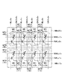
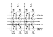
図1に本発明の第1の実施形態の回路構成を示す。本実施形態は、1Tr−1MTJ型メモリセルアレイの第1の等価回路である。MB<00>、MB<10>はそれぞれセルアレイブロックであり、一方のセルアレイブロックMB<00>には4個のメモリセルMC<00>〜MC<03>が含まれ、他方のセルアレイブロックMB<10>にも4個のメモリセルMC<10>〜MC<13>が含まれている。メモリセルMC<00>〜MC<03>、MC<10>〜MC<13>はそれぞれ磁気抵抗素子である1個の強磁性トンネル素子、即ちMTJ素子MTJ<00>〜MTJ<03>,MTJ<10>〜MTJ<13>および1個のメモリセルトランジスタMTR<00>〜MTR<03>,MTR<10>〜MTR<13>より構成される。
【0017】
セルアレイブロックMB<00>、MB<10>には4本のビット線BL<0>〜BL<3>および4本の接地側の電源線GND<0>〜GND<3>が共通に配置される。即ち、メモリセルMC<00>,MC<10>に対してビット線BL<0>、電源線GND<0>が共通に配置される。MTJ素子MTJ<00>、MTJ<10>の一端は夫々ビット線BL<0>に接続され、他端はメモリセルトランジスタMTR<00>、MTR<10>のドレイン側に夫々接続され、メモリセルトランジスタMTR<00>、MTR<10>のソース側は夫々電源線GND<0>に接続される。残りのメモリセルMC<01>〜MC<03>,MC<11>〜MC<13>も同様に接続される。
【0018】
セルアレイブロックMB<00>中のMTJ素子MTJ<00>〜MTJ<03>には共通に1本の書き込み用ワード線WWL<0>が設けられ、メモリセルトランジスタMTR<00>〜MTR<03>には共通に1本の読み出し用ワード線RWL<0>が設けられる。同様に、セルアレイブロックMB<10>中のMTJ素子MTJ<10>〜MTJ<13>にも共通に1本の書き込み用ワード線WWL<1>が設けられ、メモリセルトランジスタMTR<10>〜MTR<13>にも共通に1本の読み出し用ワード線RWL<1>が設けられる。
【0019】
なお、図中<nm>(nmは整数)はそれぞれ各メモリセルにおける<ロウ(row)カラム(column)>に対応している。
【0020】
例えば、図1に示したメモリセルMC<00>への情報の書き込みは、ビット線BL<0>と書き込み用ワード線WWL<0>に同時に電流を流すことにより発生する合成磁場によってMTJ素子MTJ<00>のフリー層のスピンの方向を制御することにより行われる。即ち、ビット線BL<0>に電流が流れると、メモリセルブロックMB<00>内のMTJ<00>のみでなく他のメモリセルブロックMB<10>内のMTJ<10>にもビット線BL<0>に流れる電流により発生された磁界が与えられる。この状態でWWL<0>に書込み電流が流れると、この電流により発生された磁界との合成磁界がMTJ素子MTJ<00>にのみ作用し、このようにして選択されたメモリセルMC<00>にのみ情報が書き込まれる。この情報の書込み時にはメモリセルトランジスタMTR<00>はオフのままであり、電源線GND<0>には電流は流れない。
【0021】
その後、情報を読み出す時は、例えば読み出し用ワード線RWL<0>が活性化することによってメモリセルトランジスタMTR<00>〜MTR<03>が同時にオンとなる。このとき、4本のビット線BL<0>〜BL<3>が同時に活性化されると、ビット線BL<0>〜BL<3>からの電流がそれぞれメモリセルトランジスタMTR<00>〜MTR<03>を介して電源線GND<0>〜GND<3>に流れ、この電流をビット線BL<0>〜BL<3>に夫々接続された図示しないセンスアンプにより検知することによりメモリセルMC<00>〜MC<03>から情報が読み出される。なお、他方のメモリセルブロックMB<10>では読み出し用ワード線RWL<1>は活性化されないので、電源線GND<0>〜GND<3>にメモリセルMC<10>〜MC<13>から同時に読み出し電流が流れ込むことはない。
【0022】
即ち、本実施形態では電源線GND<0>〜GND<3>が夫々対応するビット線BL<0>〜BL<3>と夫々1対1の関係で同一方向に配設される構成となっている。このような電源線GND<0>〜GND<3>の配設をとることにより、情報読み出し時におけるビット線BL<0>〜BL<3>から電源線GND<0>〜GND<3>に夫々流れ込む電流は、セルアレイブロックMB<00>のみで生じる。例えば一本の電源線GND<0>には対応する一本のビット線BL<0>からの電流しか流れ込まない構造となる。このため、この電源線GND<0>における電源バウンスを最小限とすることができ、その先のセンスアンプに誤作動が生じることなく確実な読み出し動作を実現する。他の電源線GND<1>〜GND<3>についても同様である。
【0023】
このような配置となっているので、図1に示した第1の実施形態のように各ビット線に対応して夫々の電源線を設けたとしても、これによりチップとして形成した場合に集積度が低下することはなく、良好な電源バウンス特性を有し、高精度の情報読み出しを保証できる半導体記憶装置を提供できる。
【0024】
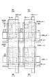
図2に図1の第1の実施形態で示された等価回路に係るMRAMの第1のレイアウト例を示す。また、図3に図2のIII―III’線で切って矢印で示す方向に見たMRAMを構成する一つのメモリセルの断面構造を示す。以下、図2,図3を参照して、本実施形態の構造、作用、効果について詳述する。
【0025】
図2は図1で示した4個のメモリセルMC<00>、MC<01>、MC<10>、MC<11>の部分のレイアウト例を示した図である。また、図3は図2のメモリセルMC<00>の部分の断面構造図である。
【0026】
図2、図3において、シリコン半導体基板SUBの表面領域にメモリセルトランジスタMTR<00>のソース拡散層DL1、ドレイン拡散層DL2が形成され、これらの拡散層DL1,DL2に跨ってシリコン半導体基板SUB表面にはゲート酸化膜Goxを介してゲート電極である書込み用ワード線RWL<0>が形成される。他のメモリセルMC<01>,MC<10>,MC<11>も同様に形成されている。
【0027】
図3において、メモリセルトランジスタMTR<00>を含む全てのメモリセルトランジスタを覆うようにシリコン半導体基板SUB上に層間絶縁膜10が堆積され、この層間絶縁膜10内に拡散層DL1,DL2に接続されたコンタクトCD1,CD2を形成するとともに層間絶縁膜10の表面に接地側の電源線GND<0>および第1配線層M0が例えば銅の埋め込み配線により形成される。この第1配線層M0は、図2に示すように、メモリセルトランジスタMTR<00>を含むメモリセルMC<00>と隣接するメモリセルMC<10>との間に形成されたスペース内に突き出すようにコンタクトCD2から延長して形成される。
【0028】
層間絶縁膜10の上には層間絶縁膜20が堆積され、この層間絶縁膜20には第1配線層M0の前記スペース内に突き出した先端部に接続されたビアV1を介して第2配線層M1が形成される。又、この第2配線層M1が形成されると同時に読み出し用ワード線RWL<0>の上方の重なり合う位置に書き込み用ワード線WWL<0>が形成される。
【0029】
層間絶縁膜20の上には層間絶縁膜30が堆積され、この層間絶縁膜30にはビアV1の上方で第2配線層M1に接続されるコンタクトCXと、このコンタクトCXに接続される第3配線層MXとが形成される。
【0030】
この第3配線層MXの上の書込み用ワード線WWL<0>と対向する位置には磁気抵抗素子としてのMTJ素子MTJ<00>が形成される。この状態で、層間絶縁膜30の上には層間絶縁膜40が形成され、この層間絶縁膜40の表面にはMTJ素子MTJ<00>を完全に覆う幅を持ったビット線BL<0>が書込み用ワード線WWL<0>と直交方向に配置される。また、図3において細い線で描かれた電源線GND<0>の層は、太線で描かれた電源線GND<0>と同じ電源線として続いており、紙面の手前から奥へ続き、図2に示したように、ビット線BL<0>と平行に電源線GND<0>が配線された様子を表わしている。
【0031】
図2に示したレイアウトでは、図1のビット線BL<0>に沿って隣接したセルアレイブロックMB<00>、MB<10>内の素子として配置されたメモリセルMC<00>とメモリセルMC<10>との間に形成されたスペースを利用して、トランジスタのドレインに接続されるコンタクトを配置している。即ち、図3を参照して説明したように、メモリセルMC<00>のメモリセルトランジスタMTR<00>のドレインとMTJ素子MTJ<00>との接続用のコンタクトCXがこのスペース内に形成される。同様に、図2に示した如く、同じスペースを利用して、メモリセルMC<10>のメモリセルトランジスタMTR<10>とMTJ素子MTJ<10>との接続用のコンタクトCXも形成される。
【0032】
このように、各メモリセルトランジスタのゲート電極の直上に対応する位置にMTJ素子を形成する場合は、書込み用のワード線をこのMTJ素子の直下に形成される例えばメタル配線を用いて配置する必要がある。このため、MTJ素子とトランジスタのドレインとを接続するためのコンタクトは、トランジスタとMTJ素子を結ぶ基板SUBに垂直な線に対してオフセットされた位置に配置することになる。そこで、図2に示すように、互いに隣接するメモリセルMC<00>、MC<10>間のスペースを利用して、夫々のメモリセル内のメモリセルトランジスタのドレインとMTJ素子との接続用のコンタクトCXが形成されている。
【0033】
更に、図2に示した例では、メモリセルトランジスタMTR<00>のゲート幅方向とビット線BL<0>の長手方向とが直交している。一方、ビット線BL<0>に対応して設けられる電源線GND<0>は隣接する2本のビット線BL<0>、BL<1>間のスペースにビット線BL<0>と同じ方向に配置される。従って、メモリセルトランジスタMTR<00>の図3に示したソース領域DL1と電源線GND<0>とを接続するために、ビット線BL<0>からT字型に分岐して形成された分岐部BGND<00>が配置されている。
例えばセルアレイブロックMB<00>内の各メモリセルMC<00>〜MC<03>へ情報を書き込む場合は、ビット線BL<0>〜BL<3>に書込むべき情報に対応する電流が流れるとともに、書込み用ワード線WWL<0>にも電流が流れる。例えば、図3に示したメモリセルMC<00>においては、ビット線BL<0>と書込み用ワード線WWL<0>に流れる電流により生成された合成磁界によりMTJ素子MTJ<00>のフリー層のスピン方向が規制され、メモリセルMC<00>に情報が書き込まれる。
【0034】
その後、情報を読み出す時は、例えば、選択されたセルアレイブロックMB<00>の読み出し用ワード線RWL<0>に電流が流れて活性化され、メモリセルトランジスタMTR<00>が導通状態となり、ビット線BL<0>からの電流が、MTJ素子MTJ<00>、配線MX、コンタクトCX、配線M1、ビアV1、配線M0、ドレインコンタクトCD2、ドレイン領域DL2、チャネル、ソース領域DL1,ソースコンタクトCD1、分岐部BGND<00>、電源線GND<0>を順次通電することによって、ビット線BL<0>に接続された図示しないセンスアンプにより情報が読み出される。このとき、メモリセルMC<00>からの読み出し電流はこのメモリセルMC<00>専用に配置された分岐部BGND<00>を介して電源線GND<0>に流れ込み、他のメモリセルからの電流は流入しないので、電源バウンスは生じない。
【0035】
図2に示したレイアウトでは、電源線GND<0>、GND<1>は夫々ビット線BL<0>、BL<1>と対応して同一方向に配設される構成となっている。このような電源線の配置をとることにより、読み出し時におけるビット線から電源線に流れ込む電流は、セルアレイブロック単位では一本の電源線には一本のビット線からの電流しか流れ込まない構造となる。このため、電源線の電源バウンスを最小限とすることができ、センスアンプに誤作動が生じるおそれが極めて小さくなり、読み出しマージンを大きく取ることができるので、確実な読み出し動作を実現する。
【0036】
また、図2のメモリセルMC<00>、MC<10>におけるコンタクトCXの配置が示すような対称的なレイアウトをとることにより、メモリセル間のスペースを有効利用し、レイアウト面積を小さくすることが出来る。
【0037】
なお、図示しないが、例えば図3においてメモリセルMC<00>のトランジスタMTR<00>の電源線GND<0>に接続されるノードであるソース拡散層DL1を、隣接するセルアレイブロック内のメモリセルのトランジスタのソース拡散層としても用いることで、2つのトランジスタ間で一つの拡散層を共有し、メモリセルのレイアウト面積を更に低減化することも可能である。これは、隣接する2つのセルアレイブロックの読み出し用ワード線が読み出し時に同時に活性化されることがなく、2個のトランジスタからの電流が同時に電源線の分岐部BGND<00>に流入することがないことから、このような配置が可能となるものである。
【0038】
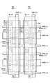
図4に図1の実施形態における第2のレイアウト例を示す。図4のレイアウトは図2のレイアウトと同様に図1での、4個のメモリセルMC<00>、MC<01>、MC<10>、MC<11>の部分のレイアウト例を示した図である。図4において図2と対応する部分には同じ参照符号を付してあり、以下、両者のレイアウト上の相違点にのみ着目して説明する。
【0039】
図2で示すレイアウトでは書込み用ワード線WWL<0>,WWL<1>と読み出し用ワード線RWL<0>,RWL<1>とが夫々メモリセルトランジスタの上方に互いに重なり合う状態で配置されている。一方、図4のレイアウトでは、読み出し用ワード線RWL<0>、RWL<1>が夫々書込み用ワード線WWL<0>、WWL<1>の真下の位置から移動され、夫々分岐部BRWL<00>,BRWL<01>,BRWL<10>,BRWL<11>の部分でT字型となっている。
【0040】
このように読み出し用ワード線RWL<0>、RWL<1>をメモリセルの部分で分岐させてT時型にすることにより、図4に示したように、各メモリセルトランジスタを図2のレイアウトに対して90度回転させて、トランジスタのゲート幅方向を電源線GND<0>,GND<1>と平行に配置できるようになる。
【0041】
このため、図3における第1配線層M0を介して接続されるドレイン側のコンタクトCXを、図4に示したように、トランジスタのゲート幅方向の近傍に配置できるようになる。また、これに伴って図2に示された分岐部BGND<00>〜BGND<11>が不用となり、電源線GND<0>、GND<1>の形状も直線となり、図2のレイアウトにおける分岐部BGND<00>〜BGND<11>のように横方向に引き出す必要がなく、パターンが単純になり、設計、プロセス上で都合がよい。また、分岐部BGND<0>などが無くなるので、メモリセル1個当たりの電源線の長さが実質的に短くなり、電源線GND<0>、GND<1>の抵抗値がより小さくなる利点もある。また、このようなビット線の長手方向とメモリセルトランジスタのゲート幅方向とを一致させる配置とすることによりメモリセルトランジスタの形成領域を長方形型のレイアウトとすることにより、ビット線に直交する方向のメモリセルアレイ面積を減少させることができ、チップ面積を低減化することも出来る。
【0042】
図4のレイアウトにおいても、電源線GND<0>、GND<1>はビット線BL<0>、BL<1>と同一方向に配設される構成となっている。このような電源線GND<0>、GND<1>の配設をとることにより、読み出し時において、例えばビット線BL<0>からは電源線GND<0>にのみ電流が流れ込み、他のビット線からは流れ込まない構造となる。このため、電源バウンスは最小限とすることができ、その先のセンスアンプに誤作動が生じることなく確実な読み出し動作を実現する。
【0043】
図5に第1の実施形態における第3のレイアウト例を示す。本レイアウトは第1の実施形態で示した4個のメモリセルMC<00>、MC<01>、MC<10>、MC<11>におけるレイアウト例を示してたものである。図5において図4に対応する部分には同一の参照符号を付してあり、以下、両者のレイアウト上の相違点にのみ着目して説明する。
【0044】
本レイアウト例では図5に示すように各メモリセルMC<00>〜MC<11>では、トランジスタのドレイン領域DL2に接続されたドレインコンタクトCD2のほぼ真上方の位置に、第1配線層M0上に積層されるビアV1、第2配線層M1、及び第2配線層M1と第3配線層MXのコンタクトCXの3層が積層されていることが特徴である。
【0045】
このようにビアV1、第2配線層M1、及びコンタクトCXの3層を、ドレインコンタクトCD2のほぼ真上方の位置に積層することが出来るのは、図4で示した第1のレイアウト例と同様にして、各メモリセルトランジスタを図2のレイアウト例と比較して90°回転させたことによる。
【0046】
つまり、図2で示すレイアウト例では、書き込み用ワード線WWL<0>、WWL<1>がドレインコンタクトCD2と重複して配置され、かつ、図3に示すように、第2配線層M1と書き込み用ワード線WWL<0>、WWL<1>はプロセス上同時に積層されるため、図5で示すレイアウト例をとることは不可能であった。しかし、図5のように各メモリセルトランジスタのゲート幅方向がビット線BL<0>、BL<1>および電源線GND<0>、GND<1>とほぼ同一方向になるように配置することにより、図4のレイアウトより更に、書き込み用ワード線WWL<0>、WWL<1>と重複しないようにドレインコンタクトCD2を形成することができるため、前記ビアV1、第2配線層M1、及びコンタクトCXの3層をその重複しないドレインコンタクトCD2のほぼ真上方に配置することが出来る。
【0047】
このような長方形型のレイアウトをとることにより、横方向のビット線に直交する方向の面積をさらに縮小することが出来るため、メモリセルアレイ面積を縮小でき、チップ面積をより縮小化することができる。また、上述のように第2配線層M1と書き込み用ワード線WWLは同時に同一のプロセスで積層されるため、パターンが単純であり、設計、プロセス、コスト面で都合が良い。
【0048】
図6に第1の実施形態における第4のレイアウト例を示す。図6は図1における4個のメモリセルMC<00>、MC<01>、MC<10>、MC<11>部分のレイアウト例を示したものである。図6において図4と対応する部分には同じ参照符号を付してあり、以下、両者のレイアウト上の相違点にのみ着目して説明する。
【0049】
図6に示すように、読み出し用ワード線RWL<1>、RWL<3>の夫々の分岐部であるBRWL<00>,BRWL<01>,BRWL<10>,BRWL<11>の他端と接続される、別に設けられた読み出し用ワード線RWL<0>、RWL<2>が、読み出し用ワード線RWL<0>、RWL<1>とほぼ同一方向に配置される。即ち、分岐部BRWL<00>〜BRWL<11>から見てH字型に配置された事が特徴である。
【0050】
つまり、メモリセルMC<00>、MC<01>においては読み出し用ワード線RWL<0>、RWL<1>の2本を用いて読み出すこととなる。同様にメモリセルMC<10>、MC<11>についても読み出し用ワード線RWL<2>、RWL<3>を用いて読み出す。
【0051】
例えばメモリセルMC<00>を読み出す場合は、両読み出し用ワード線RWL<0>、RWL<1>が活性化されて、メモリセルMC<00>およびMC<01>のメモリセルトランジスタのチャネルをオンとして、ビット線BL<0>に電流を流し、前記に示した経路により電源線GND<0>に電流を流し、その先につながった図示しないセンスアンプにより読み出しが達成される。
【0052】
このように、各メモリセルMC<00>〜MC<11>において分岐部BRWL<00>〜BRWL<11>から見た読み出し用ワード線RWL<0>〜RWL<3>をH字型とし、各メモリセル単位で読み出し用ワード線を2本に増加させることにより、確実な読み出し動作をすることが出来る。さらに、メモリセル単位で読み出し用ワード線の数が2倍となったことにより、各読み出し用ワード線RWL<0>〜RWL<3>の実効的な配線抵抗を下げ、読み出し用ワード線RWL<0>〜RWL<3>の動作速度を向上させることも出来る。
【0053】
また、この第3のレイアウト例は図2、図4、図5で示した各メモリセル単位で1本の読み出し用ワード線RWL<0>、RWL<1>で読み出すレイアウト例に比べて、各メモリセル単位で2本の読み出し用ワード線RWL<0>、RWL<1>、RWL<3>、RWL<3>を用いて読み出す。そのため、RWL<0>〜RWL<3>の実効的な抵抗が、図2、図4、図5で示したレイアウト例の読み出し用ワード線RWL<0>、RWL<1>についての抵抗値に比べて1/2となるため、図6の読み出し用ワード線RWL<0>〜RWL<3>の動作速度を上記図2、図4、図5の読み出し用ワード線RWL<0>、RWL<1>の動作速度と同じに設定すれば、メモリセルアレイの読み出し用ワード線RWL方向の規模を2倍としても同様の動作速度で読み出すことが可能となるので、チップ面積の低減、チップコストの低減が可能となる。
【0054】
図7に第1の実施形態における第5のレイアウト例を示す。図7は図1における4個のメモリセルMC<00>、MC<01>、MC<10>、MC<11>のレイアウト例を示したものである。図7において図6と対応する部分には同じ参照符号を付してあり、以下、両者のレイアウト上の相違点にのみ着目して説明する。
【0055】
本レイアウト例では図6に比べ図7に示すように各メモリセルMC<00>〜MC<11>について、ドレイン領域DL1に接続されたドレインコンタクトCD1のほぼ真上方の位置に、第1配線層M0上に積層されるビアV1、第2配線層M1、及び第2配線層M1と第3配線層MXのコンタクトCXの3層が積層されていることが特徴である。
【0056】
このようなレイアウトとすることにより、図6のレイアウト例での確実な読み出し動作等の効果を保持しつつ、さらにビット線BL<0>、BL<1>の長手方向のレイアウト面積も縮小化することが出来る。
【0057】
(第2の実施形態)
図8に本発明の第2の実施形態の回路構成を示す。本実施形態も、1Tr−1MTJ型メモリセルアレイとして構成された例である。メモリセルブロックMB<00>、MB<10>はそれぞれ共通の4本のビット線BL<0>〜BL<3>に対して構成され、一方のセルアレイブロックMB<00>には4個のメモリセルMC<00>〜MC<03>が含まれ、他方のセルアレイブロックMB<10>にも4個のメモリセルMC<10>〜MC<13>が含まれている。
【0058】
メモリセルMC<00>〜MC<03>、MC<10>〜MC<13>にはそれぞれ磁気抵抗素子である強磁性トンネル素子即ちMTJ素子MTJ<00>〜MTJ<03>,MTJ<10>〜MTJ<13>およびメモリセルトランジスタMTR<00>〜MTR<03>,MTR<10>〜MTR<13>より構成される。図8において図1と対応する部分には同じ参照符号を付してあり、以下、両者の回路構成上の相違点にのみ着目して説明する。
【0059】
本実施形態ではメモリセルブロック単位で2本のビット線に対して、1本の電源線が配置されていることが特徴である。即ち、図8のようにメモリセルブロックMB<00>では、メモリセルMC<00>、MC<01>に共通して電源線GND<0>がビット線BL<0>、BL<1>とほぼ同一方向にノードN<00>を介して配置されており、メモリセルMC<02>、MC<03>に共通して電源線GND<1>がビット線BL<0>、BL<1>とほぼ同一方向にノードN<01>を介して配置されている。
【0060】
さらに、図8のノードN<0>はメモリセルMC<00>のメモリセルトランジスタMTR<00>の一端およびメモリセルMC<01>のメモリセルトランジスタMTR<01>の一端に接続されている。同様に、ノードN<01>は夫々メモリセルMC<02>、MC<03>のメモリセルトランジスタMTR<02>、MTR<03>の一端に接続されている。メモリセルブロックMB<10>についても同様である。
【0061】
例えば、ビット線BL<0>及び書き込み用ワード線WWL<0>に電流が流され、メモリセルMC<00>について情報が書き込まれ、その後に情報を読み出す場合を考える。この読み出しは、読み出し用ワード線RWL<0>に電流が流れるとメモリセルMC<00>〜MC<03>のメモリセルトランジスタMTR<00>〜MTR<03>がオンとなり、ビット線BL<0>に電流が流され、磁気抵抗素子MTJ<00>から直列に接続されたメモリセルトランジスタMTR<00>を通ってノードN<00>を介して電源線GND<0>に電流を流し、図には示していないがこの先に接続されたセンスアンプによって読み込まれることによって行われる。他のメモリセルMC<10>〜MC<13>についても同様である。
【0062】
本実施形態では、メモリセルブロックMB<00>、MB<01>単位では、2本のビット線BL<0>とBL<1>、BL<2>とBL<3>に対して1本の電源線GND<0>、GND<1>がノード<00>〜ノードN<11>を介して配置されていることにより、図1の実施形態と比較すると、ビット線BL<0>〜BL<3>と垂直方向のセルアレイ面積を縮小することにより、チップ面積も縮小することが出来る。また、図17に示す従来の1Tr−1MTJ型メモリセルアレイの等価回路では、例えばメモリブロックMB<00>単位では、すべてのビット線BL<0>〜BL<3>からの電流が電源線GND<0>にのみ流れ込み、電源バウンスが大きく問題であった。これに対し、上述の通り本実施形態ではメモリセルブロック単位で2本のビット線に対して1本の電源線が配置されているので、電源バウンスを十分に減少させことが出来る。
【0063】
図9に第2の実施形態に係わる第1のレイアウト例を示す。図9は図8における4個のメモリセルMC<00>、MC<01>、MC<10>、MC<11>のレイアウト例を示したものである。図9において図4と対応する部分には同じ参照符号を付してあり、以下、両者のレイアウト上の相違点にのみ着目して説明する。
【0064】
図9に示すように、電源線GND<0>がビット線BL<0>、BL<1>とほぼ同一方向に配設され、ワード線方向に隣接するメモリセルMC<00>とMC<01>、MC<10>とMC<11>夫々のメモリセルトランジスタのソース領域CD1及び電源線GND<0>を共通に接続していることが特徴である。従って、図8の等価回路ではトランジスタMTR<00>とMTR<01>のソースがノードN<00>で共通に接続されているようにしめされているが、図9のレイアウトに示すように、実際には、一方のトランジスタMTR<00>のソース領域は電源線GND<0>の一方の側端部近傍に接続され、他方のトランジスタMTR<01>のソース領域は電源線GND<0>の他方の側端部近傍に接続されているので、これらの2個のトランジスタMTR<00>,MTR<01>からの電流が電源線GND<0>のある一点に集中することはない。他のノードN<01>,N<10>,N<11>に関しても同様である。
【0065】
このようなレイアウト例をとることにより、第1の実施形態における図2、図4乃至図7に示したレイアウトと比較して、ビット線BL<0>及びBL<1>の長手方向と直交する方向のレイアウト面積を縮小し、チップ面積を縮小することが出来る。
【0066】
また、本レイアウト例は電源線GND<0>の長手方向の中心線に対してビット線およびこれに関連して形成された各メモリセルが線対称となるような構造となっているので、電源線GND<0>に対して各トランジスタのソース領域DL2を共通に接続することが出来るので、同一のプロセスで積層でき、設計、プロセス、コスト等で都合が良いレイアウト例である。
【0067】
図10に第2の実施形態に係わる第2のレイアウト例を示す。図10は図8における4個のメモリセルMC<00>、MC<01>、MC<10>、MC<11>のレイアウト例を示したものである。図10において図5と対応する部分には同じ参照符号を付してあり、以下、両者のレイアウト上の相違点にのみ着目して説明する。
【0068】
図10に示すように、電源線GND<0>がビット線BL<0>、BL<1>とほぼ同一方向に配設され、ワード線方向に隣接するメモリセルMC<00>とMC<01>、MC<10>とMC<11>夫々のメモリセルトランジスタのソース領域CD1が共通に電源線GND<0>に接続されていること、及びドレイン領域DL2に接続されたドレインコンタクトCD2のほぼ真上方の位置に、第1配線層M0上に積層されるビアV1、第2配線層M1、及び第2配線層M1と第3配線層MXのコンタクトCXの3層が積層されていることが特徴である。
【0069】
このように各メモリセルにおいて前記ビアV1、第2配線層M1、コンタクトCXの3層がドレインコンタクトCD2のほぼ真上方の位置に積層されているので、図9のレイアウトと比較して、ビット線BL<0>、BL<1>の長手方向のレイアウト面積を更に縮小できる。また、本レイアウト例も図9と同様に、電源線GND<0>に対して線対称となるような構造となっているので、電源線GND<0>に対してソース領域DL1を共通に接続することが出来るので、同一のプロセスで積層でき、設計、プロセス、コスト等で都合が良いレイアウト例である。
【0070】
図11に第2の実施形態に係わる第3のレイアウト例を示す。図11は図8における4個のメモリセルMC<00>、MC<01>、MC<10>、MC<11>のレイアウト例を示したものである。図11において図6と対応する部分には同じ参照符号を付してあり、以下、両者のレイアウト上の相違点にのみ着目して説明する。
【0071】
図11に示すように、電源線GND<0>がビット線BL<0>、BL<1>とほぼ同一方向に配設され、ワード線方向に隣接するメモリセルMC<00>とMC<01>、MC<10>とMC<11>夫々のメモリセルトランジスタのソース領域CD1を電源線GND<0>と共通に接続していること、及び読み出し用ワード線RWL<1>、RWL<3>の夫々分岐部であるBRWL<00>,BRWL<01>,BRWL<10>,BRWL<11>の他端と接続される、別の読み出し用ワード線RWL<0>、RWL<2>が読み出し用ワード線RWL<0>、RWL<1>とほぼ同一方向に配置され、分岐部BRWL<00>〜BRWL<11>から見てH字型に配置された事が特徴である。
【0072】
このように、各メモリセルMC<00>〜MC<11>において分岐部BRWL<00>〜BRWL<11>から見た読み出し用ワード線RWL<0>〜RWL<3>をH字型とし、各メモリセル単位で読み出し用ワード線を2本に増加させることにより、確実な読み出し動作をすることが出来る。さらに、メモリセル単位で読み出し用ワード線数が2倍となったことにより、各読み出し用ワード線RWL<0>〜RWL<3>の実効的な配線抵抗を下げ、RWL<0>〜RWL<3>の動作速度を向上させることも出来る。
【0073】
また、本レイアウト例も電源線GND<0>に対して線対称となるような構造となっているので、電源線GND<0>に共通にソース領域DL1を接続することが出来るので、同一のプロセスで積層でき、設計、プロセス、コスト等で都合が良いレイアウト例である。
【0074】
図12に第2の実施形態に係わる第4のレイアウト例を示す。図12は図8における4個のメモリセルMC<00>、MC<01>、MC<10>、MC<11>のレイアウト例を示したものである。図12において図7と対応する部分には同じ参照符号を付してあり、以下、両者のレイアウト上の相違点にのみ着目して説明する。
【0075】
図12に示すように、読み出し用ワード線RWL<1>、RWL<3>の夫々の分岐部であるBRWL<00>,BRWL<01>,BRWL<10>,BRWL<11>の他端と接続される、別の読み出し用ワード線RWL<0>、RWL<2>が読み出し用ワード線RWL<0>、RWL<1>とほぼ同一方向であり、分岐部BRWL<00>〜BRWL<11>から見てH字型に配置された事、及びビアV1、第2配線層M1、コンタクトCXの3層がドレインコンタクトCD1のほぼ真上方の位置に積層されているのが特徴である。
【0076】
このように、各メモリセルMC<00>〜MC<11>において分岐部BRWL<00>〜BRWL<11>から見た読み出し用ワード線RWL<0>〜RWL<3>をH字型とし、各メモリセル単位で読み出し用ワード線を2本に増加させることにより、確実な読み出し動作をすることが出来る。さらに、メモリセル単位で読み出し用ワード線数が2倍となったことにより、各読み出し用ワード線RWL<0>〜RWL<3>の実効的な配線抵抗を下げ、RWL<0>〜RWL<3>の動作速度を向上させることも出来る。
【0077】
また、各メモリセルにおいて前記ビアV1、第2配線層M1、コンタクトCXの3層が一つのドレインコンタクトCD1のほぼ真上方の位置に積層されているので、図11のレイアウトと比較して、ビット線BL<0>、BL<1>の長手方向のレイアウト面積を縮小できる。
【0078】
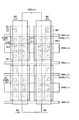
(第3の実施形態)
図13に本発明の第3の実施形態の回路構成を示す。本実施形態は、1Tr−1MTJ型メモリセルアレイとして構成した例である。図13において、一方のセルアレイブロックMB<00>には4個のメモリセルMC<00>〜MC<03>が含まれ、他方のセルアレイブロックMB<10>にも4個のメモリセルMC<10>〜MC<13>が含まれている。メモリセルMC<00>〜MC<03>、MC<10>〜MC<13>にはそれぞれ磁気抵抗素子である1個の強磁性トンネル素子即ちMTJ素子MTJ<00>〜MTJ<03>,MTJ<10>〜MTJ<13>および1個のメモリセルトランジスタMTR<00>〜MTR<03>,MTR<10>〜MTR<13>が含まれる。
【0079】
図13において図8と対応する部分には同じ参照符号を付してあり、以下、両者の回路構成上の相違点にのみ着目して説明する。
【0080】
本実施形態ではメモリセルブロックMB<00>,MB<10>に夫々書込み用、読み出し用のワード線とほぼ同一方向に新たな電源線GND<10>、GND<11>が夫々加えられ、4本のビット線BL<0>〜BL<3>に対して、各メモリセルブロックに3本の電源線が配置されていることが特徴である。
【0081】
即ち、図13のようにメモリセルブロックMB<00>では、メモリセルMC<00>とMC<01>のメモリセルトランジスタMTR<00>、MTR<01>の一端が夫々ノードN<00>、ノードN<02>を介して電源線GND<10>に接続され、さらに電源線GND<00>がノードN<01>を介して電源線GND<10>に接続されている。また、メモリセルMC<02>とMC<03>のメモリセルトランジスタMTR<02>、MTR<03>の一端が夫々ノードN<03>、ノードN<05>を介して電源線GND<10>に接続され、さらに電源線GND<01>がノードN<04>を介して電源線GND<10>接続されている。
【0082】
さらに、図13に示すようにノードN<00>は、メモリセルMC<00>のメモリセルトランジスタMTR<00>の一端、メモリセルMC<01>のメモリセルトランジスタMTR<01>の一端、電源線GND<00>、及び電源線GND<10>に接続されている。ノードN<03>はメモリセルMC<02>のメモリセルトランジスタMTR<02>の一端、メモリセルMC<03>のメモリセルトランジスタMTR<03>の一端、電源線GND<01>、及び電源線GND<10>に接続されている。メモリセルブロックMB<10>についても同様である。
【0083】
例えば、ビット線BL<0>及び書き込み用ワード線WWL<0>に電流を流し、メモリセルMC<00>について情報が書き込まれ、その後に情報を読み出す場合は、読み出し用ワード線RWL<0>に電流が流れるとメモリセルMC<00>〜MC<03>のメモリセルトランジスタMTR<00>〜MTR<03>がオンとなり、ビット線BL<0>に電流が流され、磁気抵抗素子MTJ<00>から直列に接続されたメモリセルトランジスタMTR<00>を通ってノードN<00>を介して電源線GND<0>及び電源線GND<10>に電流を流し、図には示していないがこの先に接続されたセンスアンプによって読み込まれることによって行われる。他のメモリセルMC<01>〜MC<13>についても同様である。
【0084】
本実施形態では、メモリセルブロックMB<00>単位では、2本のビット線BL<0>とBL<1>、BL<2>とBL<3>に対して3本の電源線GND<00>、GND<01>、GND<11>がノードN<00>、ノードN<04>を介して配置されていることにより、ビット線BL<0>〜BL<3>から電源線GND<00>,GND<01>に流入する電流を更に電源線GND<10>に分散させることができる。メモリセルブロックMB<10>に設けられた3本目の電源線GND<11>についても同様である。
【0085】
上述の通り本実施形態ではメモリセルブロック単位で4本のビット線に対して3本の電源線が配置されているので、電源バウンスを十分に減少させることが出来る。
【0086】
(第4の実施形態)
図14に本発明の第4の実施形態の回路構成を示す。本実施形態は、1Tr−1MTJ型メモリセルアレイとして構成されている。メモリセルブロックMB<10>、MB<20>のレイアウト例は図15に示す。一方のセルアレイブロックMB<10>には4個のメモリセルMC<10>〜MC<13>が含まれ、他方のセルアレイブロックMB<20>にも4個のメモリセルMC<20>〜MC<23>が含まれている。メモリセルMC<10>〜MC<13>、MC<20>〜MC<23>は、それぞれ磁気抵抗素子である1個の強磁性トンネル素子即ちMTJ素子MTJ<10>〜MTJ<13>,MTJ<20>〜MTJ<23>および1個のメモリセルトランジスタMTR<10>〜MTR<13>,MTR<20>〜MTR<23>より構成される。図14において図8と対応する部分には同じ参照符号を付してあり、以下、両者の回路構成上の相違点にのみ着目して説明する。
【0087】
本実施形態では、図13の実施形態におけるセルアレイブロックMB<00>,MB<10>夫々に対応して設けられた2本の電源線GND<10>,GND<11>を、2つのセルアレイブロックに対して1本に纏めて用いられる。このため、一方のセルアレイブロックMB<00>のメモリセルトランジスタのソースと他方のセルアレイブロックMB<10>のメモリセルトランジスタのソースとを互いに近接配置することがレイアウト上で重要となる。
【0088】
即ち、図14において、2つのセルアレイブロックMB<10>,MB<20>に対して、ワード線WWL<1>、WWL<2>、RWL<1>、RWL<2>とほぼ同一方向でさらにビット線BL<0>〜BL<3>に沿って隣接する各メモリセルトランジスタMTR<10>〜MTR<23>の一端、及び電源線GND<00>、GND<01>に共通の電源線GND<11>を配設したことが特徴である。
【0089】
即ち、図14のようにメモリセルブロックMB<10>では、メモリセルMC<10>のメモリセルトランジスタMTR<10>の一端がノードN<10>を介して、メモリセルMC<11>ではトランジスタMTR<11>の一端がノードN<12>を介して電源線GND<11>に接続され、さらに電源線GND<00>がノードN<11>を介して電源線GND<11>接続されている。
【0090】
また、メモリセルMC<12>ではメモリセルトランジスタMTR<12>の一端がノードN<13>を介して、メモリセルMC<13>ではノードN<15>を介して電源線GND<11>に接続され、さらに電源線GND<01>がノードN<14>を介して電源線GND<11>に接続されていることが特徴である。また、メモリセルブロックMB<20>についても夫々のメモリセルトランジスタが同じノードを介して電源線GND<11>に接続されるとともに、電源線GND<00>,GND<01>と共通に接続される。
【0091】
例えば、ビット線BL<0>及び書き込み用ワード線WWL<1>に電流が流され、メモリセルMC<10>について情報が書き込まれ、その後に情報を読み出す場合は、読み出し用ワード線RWL<1>に電流が流れるとメモリセルMC<10>〜MC<13>のメモリセルトランジスタMTR<10>〜MTR<13>がオンとなり、例えばビット線BL<0>に電流が流され、磁気抵抗素子MTJ<10>から直列に接続されたメモリセルトランジスタMTR<10>を通ってノードN<10>を介して電源線GND<00>及び電源線GND<11>に電流を流し、図には示していないがこの先に接続されたセンスアンプによって情報が読み出される。他のメモリセルMC<11>〜MC<23>についても同様である。
【0092】
本実施形態では、各メモリセルブロックMB<10>、MB<20>単位では、2本のビット線BL<0>とBL<1>、BL<2>とBL<3>に対して実質的に3本の電源線GND<00>、GND<01>、GND<11>がノードN<10>〜ノードN<15>を介して配置されていることにより、図13の実施態様と同様に電源バウンスを軽減できると共に、ビット線BL<0>〜BL<3>の長手方向の電源線の本数が減少するため、セルアレイ面積を更に縮小することが出来る。
【0093】
図15は図14の第4の実施形態に係わるレイアウト例を示す。図15は図14における4個のメモリセルMC<10>、MC<11>、MC<20>、MC<21>およびこれらのメモリセルMC<10>〜MC<21>を最小単位のレイアウトとしてビット線BL<0>、BL<1>と同一方向に続くべき2個のメモリセルMC<00>、MC<01>のレイアウト例を示したものである。図15において図2と対応する部分には同じ参照符号を付してあり、以下、両者のレイアウト上の相違点にのみ着目して説明する。
【0094】
図15に示したレイアウト例では、ビット線BL<0>に沿って隣接したセルアレイブロックMB<00>、MB<10>内の素子として配置されたメモリセルMC<00>とメモリセルMC<10>との間に形成されたスペースを利用して、夫々のメモリセルのトランジスタのドレインに接続されるコンタクトを配置している。即ち、図3を参照して説明したように、メモリセルMC<00>のメモリセルトランジスタMTR<00>のドレインDL2とMTJ素子MTJ<00>との接続用のコンタクトCXがこのスペース内に形成される。同様に、同じスペースを利用して、メモリセルMC<10>のメモリセルトランジスタMTR<10>とMTJ素子MTJ<10>との接続用のコンタクトCXが形成されることは図2で示したレイアウト例と同様である。
【0095】
しかし、さらに本レイアウト例では、書き込み用ワード線WWL<0>〜WWL<2>及び読み出し用ワード線RWL<0>〜RWL<3>に沿って隣接するメモリセルMC<10>とMC<20>、メモリセルMC<11>とMC<21>のワード線とほぼ同一方向の共通の電源線GND<11>を配設したことが特徴である。
【0096】
このように、電源線GND<11>をワード線に沿って隣接するメモリセルMC<10>〜MC<21>で共有するので、ビット線BL<0>、BL<1>の長手方向のレイアウト面積を縮小できる。また、電源線GND<11>に対してメモリセルMC<10>〜MC<21>のソース領域DL1を共通に接続することが出来るので、同一のプロセスで積層でき、設計、プロセス、コスト等で都合が良いという効果を有する。
【0097】
尚、以上の各実施形態では磁気抵抗素子としてMTJ素子を用いた例を示したが、磁気抵抗素子として例えばGMR(Giant magneto resistive)素子等を用いても同様の効果を得ることが出来る。
【0098】
【発明の効果】
以上詳述したようにこの発明によれば、電源線の電源バウンスを最小化し、読み出しマージンが向上する半導体記憶装置を提供することが出来る。
【図面の簡単な説明】
【図1】本発明第の1の実施形態に係わる1Tr−1MTJ型メモリセルアレイの第1の等価回路図。
【図2】第1の実施形態に係るMRAMの第1のレイアウト例。
【図3】図2のIII―III’線で切って矢印で示す方向に見たMRAMのメモリセルの断面構造を示す断面図。
【図4】第1の実施形態に係わる第2のレイアウト例。
【図5】第1の実施形態に係わる第3のレイアウト例。
【図6】第1の実施形態に係わる第4のレイアウト例。
【図7】第1の実施形態に係わる第5のレイアウト例。
【図8】本発明の第2の実施形態に係わる1Tr−1MTJ型メモリセルアレイの第2の等価回路図。
【図9】第2の実施形態に係わる第1のレイアウト例。
【図10】第2の実施形態に係わる第2のレイアウト例。
【図11】第2の実施形態に係わる第3のレイアウト例。
【図12】第2の実施形態に係わる第4のレイアウト例。
【図13】本発明の第3の実施形態に係わる1Tr−1MTJ型メモリセルアレイの第3の等価回路図。
【図14】本発明の第4の実施形態に係わる1Tr−1MTJ型メモリセルアレイの第4の等価回路図。
【図15】第4の実施形態に係わるレイアウト例。
【図16】従来の1Tr−1MTJ型メモリセルの等価回路図。
【図17】従来の1Tr−1MTJ型メモリセルアレイの第1の等価回路図。
【図18】図17の等価回路に係わるレイアウト例。
【図19】従来の1Tr−1MTJ型メモリセルの断面構造図。
【図20】従来の1Tr−1MTJ型メモリセルアレイの第2の等価回路図。
【図21】図20の等価回路に係わるレイアウト例。
【符号の説明】
MB<00>、MB<10>,MB<20> … セルアレイブロック、
MC<00>〜MC<23> … メモリセル、
MTJ<00>〜MTJ<23> … 強磁性トンネル素子、
MTR<00>〜MTR<23> … メモリセルトランジスタ、
BL<0>〜BL<3> … ビット線、
WWL<0>〜WWL<2> … 書き込み用ワード線、
RWL<0>〜RWL<2> … 読み出し用ワード線、
GND<0>、GND<1> … 電源線。[0001]
TECHNICAL FIELD OF THE INVENTION
The present invention relates to a semiconductor memory device having a configuration in which a current flows into a power supply line via a memory cell when reading stored data.
[0002]
[Prior art]
In recent years, as a memory device that can be replaced with a DRAM, an EEPROM, or the like, an MRAM configured using a magnetoresistive element having non-volatility, high-speed operation, high integration, and high reliability is expected, and its development is proceeding. (For example, see Non-Patent
[0003]
[Non-patent document 1]
ISSCC Proceedings TA7.2, pp128-129
[0004]
[Non-patent document 2]
ISSCC Proceedings TA7.3, pp130-131
As the magnetoresistive element, there are a GMR (Giant Magneto Resistive) element utilizing a magnetoresistance change due to a spin-polarized tunnel effect in a magnetic / insulator laminated structure, an MTJ (Magnetic Tunnel Junction) element, and the like. The MRAM using is promising.
[0005]
The MTJ element has a structure in which one ferromagnetic film sandwiches one insulating film, and a tunnel current is generated when the spin directions of the ferromagnetic films are parallel and antiparallel. It has the characteristic that the size of changes. When the spin directions are parallel, the resistance of the MTJ element is low because the tunnel current is large, and when the spin directions are antiparallel, the resistance of the MTJ element is low because the tunnel current is small. Get higher. In the MRAM, information is recorded as “0” data when the resistance value of the MTJ element is low, and as “1” data when the resistance value is high.
[0006]
FIG. 16 shows an equivalent circuit of one typical 1Tr-1 MTJ type memory cell of an MRAM using the MTJ element, and FIG. 17 shows an equivalent circuit of the memory cell array. Symbols in the figure are MB for a cell array block, MC for a memory cell, MTR for a memory cell transistor, GND for a ground electrode line, that is, a power supply line, BL for a bit line, WWL for a write word line, and RWL for a read word. Represents a line. <Nm> (nm is an integer) indicates <row column> in the memory cell.
[0007]
18 is a layout example of FIG. 17, and FIG. 19 is a cross-sectional structure diagram of a 1Tr-1MTJ type memory cell according to the related art. The symbols in the drawing mean that Gox is a gate insulating film, DL is a diffusion film, RWL is a read word line, MO is a first wiring layer, GND is a power supply line, M1 is a second wiring layer, and WWL is a write word. Line, CD is a contact from M0 to DL, V1 is a contact from M1 to M0, MTJ is a ferromagnetic tunnel junction element, MX is a wiring layer for MTJ connection, and CX is a contact from MX to M1.
[0008]
FIG. 20 is a circuit diagram in which GND between adjacent rows in the equivalent circuit of FIG. 17 is shared. FIG. 21 is a layout example of FIG.
[0009]
As shown in FIG. 17, FIG. 18, FIG. 19, FIG. 20, and FIG. 21, BL and WWL are wired in the orthogonal direction, and when writing information to a memory cell, a combined magnetic field is generated by applying a current to BL and WWL. And write the information. When reading information from a memory cell, RWL is activated, a current flows from BL to GND, and information is read by a sense amplifier connected to BL.
[0010]
However, the conventional power line wiring has the following problems.
[0011]
[Problems to be solved by the invention]
As shown in FIGS. 17 and 20, all of the conventional GNDs are wired in the same direction as RWL / WWL, and the memory cells are separated for each row. In such a configuration, currents from all the BLs in one memory cell array block flow into one GND wiring during a read operation, so that a large current flows through one GND wiring. There is a problem that a so-called power bounce occurs.
[0012]
SUMMARY OF THE INVENTION It is an object of the present invention to provide a semiconductor memory device that minimizes power bounce on a power line and improves a read margin.
[0013]
[Means for Solving the Problems]
The semiconductor memory device of the present invention has at least one cell array block including a memory cell including a plurality of magneto-resistive elements, and the cell array block includes a word line and at least a read operation performed simultaneously by the word line. A plurality of selected memory cells, a plurality of power supply lines connected to one end of each of the selected plurality of memory cells, and a plurality of bit lines connected to the other end of each of the plurality of memory cells. It is characterized by having.
[0014]
With this configuration, it is possible to provide a semiconductor memory device that minimizes power bounce in a power line and improves a read margin.
[0015]
BEST MODE FOR CARRYING OUT THE INVENTION
Hereinafter, embodiments of the present invention will be described with reference to the drawings.
[0016]
(1st Embodiment)
FIG. 1 shows a circuit configuration of the first embodiment of the present invention. This embodiment is a first equivalent circuit of a 1Tr-1MTJ type memory cell array. MB <00> and MB <10> are cell array blocks, respectively. One cell array block MB <00> includes four memory cells MC <00> to MC <03> and the other cell array block MB <10> also includes four memory cells MC <10> to MC <13>. Each of the memory cells MC <00> to MC <03> and MC <10> to MC <13> is one ferromagnetic tunnel element which is a magnetoresistive element, that is, MTJ elements MTJ <00> to MTJ <03>, MTJ. <10> to MTJ <13> and one memory cell transistor MTR <00> to MTR <03>, MTR <10> to MTR <13>.
[0017]
In the cell array blocks MB <00> and MB <10>, four bit lines BL <0> to BL <3> and four ground-side power supply lines GND <0> to GND <3> are commonly arranged. You. That is, the bit line BL <0> and the power supply line GND <0> are commonly arranged for the memory cells MC <00> and MC <10>. One end of each of the MTJ elements MTJ <00> and MTJ <10> is connected to the bit line BL <0>, and the other end is connected to the drain side of the memory cell transistors MTR <00> and MTR <10>, respectively. The sources of the transistors MTR <00> and MTR <10> are connected to the power supply line GND <0>, respectively. The remaining memory cells MC <01> to MC <03> and MC <11> to MC <13> are similarly connected.
[0018]
One write word line WWL <0> is commonly provided to the MTJ elements MTJ <00> to MTJ <03> in the cell array block MB <00>, and the memory cell transistors MTR <00> to MTR <03> are provided. Are commonly provided with one read word line RWL <0>. Similarly, one write word line WWL <1> is commonly provided for the MTJ elements MTJ <10> to MTJ <13> in the cell array block MB <10>, and the memory cell transistors MTR <10> to MTR are provided. One read word line RWL <1> is commonly provided for <13>.
[0019]
In the drawing, <nm> (nm is an integer) respectively corresponds to <row column> in each memory cell.
[0020]
For example, writing of information to the memory cell MC <00> shown in FIG. 1 is performed by the MTJ element MTJ by a combined magnetic field generated by applying current to the bit line BL <0> and the write word line WWL <0> simultaneously. This is performed by controlling the direction of spin of the free layer of <00>. That is, when a current flows through the bit line BL <0>, the bit line BL is transmitted not only to the MTJ <00> in the memory cell block MB <00> but also to the MTJ <10> in another memory cell block MB <10>. A magnetic field generated by a current flowing through <0> is applied. When a write current flows through WWL <0> in this state, a combined magnetic field with a magnetic field generated by this current acts only on MTJ element MTJ <00>, and thus selected memory cell MC <00>. Information is written only to At the time of writing this information, the memory cell transistor MTR <00> remains off, and no current flows through the power supply line GND <0>.
[0021]
Thereafter, when reading information, the memory cell transistors MTR <00> to MTR <03> are simultaneously turned on, for example, by activating the read word line RWL <0>. At this time, when the four bit lines BL <0> to BL <3> are activated at the same time, currents from bit lines BL <0> to BL <3> are applied to memory cell transistors MTR <00> to MTR, respectively. The current flows through the power supply lines GND <0> to GND <3> via <03>, and the current is detected by sense amplifiers (not shown) connected to the bit lines BL <0> to BL <3>, respectively. Information is read from MC <00> to MC <03>. In the other memory cell block MB <10>, the read word line RWL <1> is not activated, so that the power supply lines GND <0> to GND <3> are connected to the memory cells MC <10> to MC <13>. The read current does not flow at the same time.
[0022]
That is, in this embodiment, the power supply lines GND <0> to GND <3> are arranged in the same direction with the corresponding bit lines BL <0> to BL <3> in a one-to-one relationship. ing. By providing such power supply lines GND <0> to GND <3>, bit lines BL <0> to BL <3> can be changed from power supply lines GND <0> to GND <3> during information reading. The respective currents flow in only the cell array block MB <00>. For example, a structure in which only one current from one corresponding bit line BL <0> flows into one power supply line GND <0>. For this reason, the power supply bounce on the power supply line GND <0> can be minimized, and a reliable read operation can be realized without causing a malfunction in the subsequent sense amplifier. The same applies to other power supply lines GND <1> to GND <3>.
[0023]
With such an arrangement, even if each power line is provided corresponding to each bit line as in the first embodiment shown in FIG. Thus, it is possible to provide a semiconductor memory device that has good power bounce characteristics without deterioration and that can guarantee highly accurate information reading.
[0024]
FIG. 2 shows a first layout example of the MRAM according to the equivalent circuit shown in the first embodiment of FIG. FIG. 3 shows a cross-sectional structure of one memory cell constituting the MRAM as viewed in a direction indicated by an arrow by cutting along a line III-III 'in FIG. Hereinafter, the structure, operation, and effect of the present embodiment will be described in detail with reference to FIGS.
[0025]
FIG. 2 is a diagram showing a layout example of the four memory cells MC <00>, MC <01>, MC <10>, and MC <11> shown in FIG. FIG. 3 is a sectional structural view of a memory cell MC <00> in FIG.
[0026]
2 and 3, the source diffusion layer DL1 and the drain diffusion layer DL2 of the memory cell transistor MTR <00> are formed in the surface region of the silicon semiconductor substrate SUB, and the silicon semiconductor substrate SUB extends over these diffusion layers DL1 and DL2. A write word line RWL <0> as a gate electrode is formed on the surface via a gate oxide film Gox. Other memory cells MC <01>, MC <10>, and MC <11> are similarly formed.
[0027]
3, an
[0028]
An interlayer insulating
[0029]
An interlayer insulating
[0030]
An MTJ element MTJ <00> as a magnetoresistive element is formed on the third wiring layer MX at a position facing the write word line WWL <0>. In this state, an
[0031]
In the layout shown in FIG. 2, memory cells MC <00> and MC arranged as elements in adjacent cell array blocks MB <00> and MB <10> along bit line BL <0> in FIG. The contact connected to the drain of the transistor is arranged by utilizing the space formed between <10>. That is, as described with reference to FIG. 3, the contact CX for connection between the drain of the memory cell transistor MTR <00> of the memory cell MC <00> and the MTJ element MTJ <00> is formed in this space. You. Similarly, as shown in FIG. 2, a contact CX for connection between the memory cell transistor MTR <10> of the memory cell MC <10> and the MTJ element MTJ <10> is formed using the same space.
[0032]
As described above, when the MTJ element is formed at a position directly above the gate electrode of each memory cell transistor, it is necessary to arrange a write word line using, for example, a metal wiring formed immediately below the MTJ element. There is. For this reason, the contact for connecting the MTJ element and the drain of the transistor is arranged at a position offset with respect to a line perpendicular to the substrate SUB connecting the transistor and the MTJ element. Therefore, as shown in FIG. 2, the space between the memory cells MC <00> and MC <10> adjacent to each other is used to connect the MTJ element to the drain of the memory cell transistor in each memory cell. The contact CX is formed.
[0033]
Further, in the example shown in FIG. 2, the gate width direction of the memory cell transistor MTR <00> is orthogonal to the longitudinal direction of the bit line BL <0>. On the other hand, the power supply line GND <0> provided corresponding to the bit line BL <0> is provided in the space between the two adjacent bit lines BL <0> and BL <1> in the same direction as the bit line BL <0>. Placed in Therefore, in order to connect the source region DL1 of the memory cell transistor MTR <00> shown in FIG. 3 to the power supply line GND <0>, a branch formed by branching from the bit line BL <0> into a T shape. The section BGND <00> is arranged.
For example, when writing information to each of the memory cells MC <00> to MC <03> in the cell array block MB <00>, a current corresponding to the information to be written to the bit lines BL <0> to BL <3> flows. At the same time, a current also flows through the write word line WWL <0>. For example, in the memory cell MC <00> shown in FIG. 3, the free layer of the MTJ element MTJ <00> is generated by a combined magnetic field generated by a current flowing through the bit line BL <0> and the write word line WWL <0>. Is regulated, and information is written to the memory cell MC <00>.
[0034]
Thereafter, when reading information, for example, a current flows through the read word line RWL <0> of the selected cell array block MB <00> to be activated, the memory cell transistor MTR <00> is turned on, and the bit is turned on. When the current from the line BL <0> is the MTJ element MTJ <00>, the wiring MX, the contact CX, the wiring M1, the via V1, the wiring M0, the drain contact CD2, the drain region DL2, the channel, the source region DL1, the source contact CD1, By sequentially energizing the branch part BGND <00> and the power supply line GND <0>, information is read by a sense amplifier (not shown) connected to the bit line BL <0>. At this time, the read current from the memory cell MC <00> flows into the power supply line GND <0> via the branching section BGND <00> dedicated to the memory cell MC <00>, and the read current from another memory cell MC <00>. Since no current flows, no power bounce occurs.
[0035]
In the layout shown in FIG. 2, the power supply lines GND <0> and GND <1> are arranged in the same direction as the bit lines BL <0> and BL <1>, respectively. By arranging such power supply lines, a current flowing from the bit line to the power supply line at the time of reading has a structure in which only one current flows from one bit line to one power supply line in a cell array block unit. . For this reason, the power bounce of the power supply line can be minimized, the possibility that a malfunction occurs in the sense amplifier is extremely reduced, and a large read margin can be taken, so that a reliable read operation is realized.
[0036]
In addition, by taking a symmetrical layout as shown by the arrangement of the contacts CX in the memory cells MC <00> and MC <10> in FIG. 2, the space between the memory cells is effectively used, and the layout area is reduced. Can be done.
[0037]
Although not shown, for example, in FIG. 3, the source diffusion layer DL1 which is a node connected to the power supply line GND <0> of the transistor MTR <00> of the memory cell MC <00> is connected to the memory cell MC in the adjacent cell array block. , It is possible to share one diffusion layer between the two transistors and further reduce the layout area of the memory cell. This is because the read word lines of two adjacent cell array blocks are not activated at the same time at the time of reading, and currents from two transistors do not simultaneously flow into the branch portion BGND <00> of the power supply line. Thus, such an arrangement becomes possible.
[0038]
FIG. 4 shows a second layout example in the embodiment of FIG. 4 is a diagram showing a layout example of a portion of four memory cells MC <00>, MC <01>, MC <10>, and MC <11> in FIG. 1 similarly to the layout of FIG. It is. 4, parts corresponding to those in FIG. 2 are denoted by the same reference numerals, and the following description will be made by focusing only on differences in layout between the two.
[0039]
In the layout shown in FIG. 2, write word lines WWL <0>, WWL <1> and read word lines RWL <0>, RWL <1> are arranged above memory cell transistors so as to overlap each other. . On the other hand, in the layout of FIG. 4, the read word lines RWL <0>, RWL <1> are moved from the positions directly below the write word lines WWL <0>, WWL <1>, respectively, and the branch portions BRWL <00, respectively. >, BRWL <01>, BRWL <10>, and BRWL <11> are T-shaped.
[0040]
In this manner, the read word lines RWL <0> and RWL <1> are branched at the memory cell portion to form the T-time type, so that each memory cell transistor is arranged as shown in FIG. , The gate width direction of the transistor can be arranged in parallel with the power supply lines GND <0> and GND <1>.
[0041]
Therefore, the contact CX on the drain side connected via the first wiring layer M0 in FIG. 3 can be arranged near the transistor in the gate width direction as shown in FIG. In addition, the branch portions BGND <00> to BGND <11> shown in FIG. 2 are unnecessary, and the shapes of the power supply lines GND <0> and GND <1> are also straight lines. There is no need to draw out in the horizontal direction as in the sections BGND <00> to BGND <11>, and the pattern becomes simple, which is convenient in design and process. Further, since the branch part BGND <0> is eliminated, the length of the power supply line per memory cell is substantially shortened, and the resistance of the power supply lines GND <0> and GND <1> is further reduced. There is also. Further, by arranging the longitudinal direction of such a bit line and the gate width direction of the memory cell transistor so that the memory cell transistor formation region has a rectangular layout, the memory cell transistor can be formed in a direction orthogonal to the bit line. The area of the memory cell array can be reduced, and the chip area can be reduced.
[0042]
In the layout of FIG. 4 as well, power supply lines GND <0> and GND <1> are arranged in the same direction as bit lines BL <0> and BL <1>. By arranging such power supply lines GND <0> and GND <1>, at the time of reading, for example, current flows only from the bit line BL <0> to the power supply line GND <0>, and other bits The structure does not flow from the wire. For this reason, power bounce can be minimized, and a reliable read operation can be realized without a malfunction occurring in the sense amplifier ahead.
[0043]
FIG. 5 shows a third layout example in the first embodiment. This layout shows a layout example of the four memory cells MC <00>, MC <01>, MC <10>, and MC <11> shown in the first embodiment. In FIG. 5, portions corresponding to those in FIG. 4 are denoted by the same reference numerals, and the following description will be made focusing only on the layout differences between the two.
[0044]
In this layout example, as shown in FIG. 5, in each of the memory cells MC <00> to MC <11>, the first wiring layer M0 is located almost directly above the drain contact CD2 connected to the drain region DL2 of the transistor. Is characterized in that three layers of a via V1, a second wiring layer M1, and a contact CX of the second wiring layer M1 and the third wiring layer MX are stacked.
[0045]
As described above, the three layers of the via V1, the second wiring layer M1, and the contact CX can be stacked almost directly above the drain contact CD2, as in the first layout example shown in FIG. This is because each memory cell transistor is rotated by 90 ° as compared with the layout example of FIG.
[0046]
That is, in the layout example shown in FIG. 2, the write word lines WWL <0> and WWL <1> are arranged so as to overlap with the drain contact CD2, and as shown in FIG. Since the use word lines WWL <0> and WWL <1> are simultaneously laminated in the process, the layout example shown in FIG. 5 cannot be taken. However, as shown in FIG. 5, each memory cell transistor is arranged such that the gate width direction is substantially the same as the bit lines BL <0> and BL <1> and the power supply lines GND <0> and GND <1>. 4, the drain contact CD2 can be formed so as not to overlap with the write word lines WWL <0> and WWL <1>, so that the via V1, the second wiring layer M1, and the contact The three layers of CX can be arranged almost directly above the non-overlapping drain contact CD2.
[0047]
By adopting such a rectangular layout, the area in the direction orthogonal to the horizontal bit lines can be further reduced, so that the memory cell array area can be reduced and the chip area can be further reduced. Further, as described above, since the second wiring layer M1 and the write word line WWL are simultaneously laminated in the same process, the pattern is simple, which is convenient in terms of design, process, and cost.
[0048]
FIG. 6 shows a fourth layout example in the first embodiment. FIG. 6 shows a layout example of four memory cells MC <00>, MC <01>, MC <10>, and MC <11> in FIG. 6, parts corresponding to those in FIG. 4 are denoted by the same reference numerals, and the following description will be made by focusing only on the layout differences between the two.
[0049]
As shown in FIG. 6, the other ends of BRWL <00>, BRWL <01>, BRWL <10>, and BRWL <11>, which are branch portions of the read word lines RWL <1> and RWL <3>, respectively. The connected read word lines RWL <0> and RWL <2> provided separately are arranged in substantially the same direction as the read word lines RWL <0> and RWL <1>. That is, it is characterized in that it is arranged in an H shape when viewed from the branch portions BRWL <00> to BRWL <11>.
[0050]
That is, in the memory cells MC <00> and MC <01>, reading is performed using two read word lines RWL <0> and RWL <1>. Similarly, the memory cells MC <10> and MC <11> are read using the read word lines RWL <2> and RWL <3>.
[0051]
For example, when reading the memory cell MC <00>, both read word lines RWL <0> and RWL <1> are activated, and the channels of the memory cell transistors of the memory cells MC <00> and MC <01> are changed. When turned on, a current flows through the bit line BL <0>, a current flows through the power supply line GND <0> through the above-described path, and reading is achieved by a sense amplifier (not shown) connected to the power supply line GND <0>.
[0052]
As described above, in each of the memory cells MC <00> to MC <11>, the read word lines RWL <0> to RWL <3> viewed from the branch portions BRWL <00> to BRWL <11> are H-shaped, By increasing the number of read word lines for each memory cell to two, a reliable read operation can be performed. Further, since the number of read word lines is doubled for each memory cell, the effective wiring resistance of each of the read word lines RWL <0> to RWL <3> is reduced, and the read word lines RWL <0> to RWL <3>.
[0053]
Further, the third layout example is different from the layout example in which one read word line RWL <0> and one read word line RWL <1> are read for each memory cell unit shown in FIGS. Reading is performed using two read word lines RWL <0>, RWL <1>, RWL <3>, and RWL <3> in units of memory cells. Therefore, the effective resistance of RWL <0> to RWL <3> is changed to the resistance value of the read word lines RWL <0> and RWL <1> in the layout examples shown in FIGS. The operation speed of the read word lines RWL <0> to RWL <3> in FIG. 6 is reduced by half compared with the operation speed of the read word lines RWL <0> and RWL <in FIG. 2, FIG. 4, and FIG. If the operation speed is set to be the same as 1>, it is possible to read at the same operation speed even if the scale of the memory cell array in the direction of the read word line RWL is doubled, so that the chip area and chip cost are reduced. Becomes possible.
[0054]
FIG. 7 shows a fifth layout example according to the first embodiment. FIG. 7 shows a layout example of four memory cells MC <00>, MC <01>, MC <10>, and MC <11> in FIG. In FIG. 7, portions corresponding to those in FIG. 6 are denoted by the same reference numerals, and the following description will be made focusing on only the layout differences.
[0055]
In the present layout example, as shown in FIG. 7, as compared to FIG. 6, for each of the memory cells MC <00> to MC <11>, the first wiring layer is located almost directly above the drain contact CD1 connected to the drain region DL1. It is characterized in that three layers of a via V1, a second wiring layer M1, and a contact CX of the second wiring layer M1 and the third wiring layer MX are stacked on M0.
[0056]
With such a layout, the layout area in the longitudinal direction of the bit lines BL <0> and BL <1> is further reduced while maintaining the effect of the reliable read operation and the like in the layout example of FIG. I can do it.
[0057]
(Second embodiment)
FIG. 8 shows a circuit configuration of the second embodiment of the present invention. This embodiment is also an example configured as a 1Tr-1MTJ type memory cell array. Each of memory cell blocks MB <00> and MB <10> is configured for four common bit lines BL <0> to BL <3>, and one cell array block MB <00> has four memories. The cells MC <00> to MC <03> are included, and the other cell array block MB <10> also includes four memory cells MC <10> to MC <13>.
[0058]
Each of the memory cells MC <00> to MC <03> and MC <10> to MC <13> has a ferromagnetic tunnel element, which is a magnetoresistive element, that is, an MTJ element MTJ <00> to MTJ <03>, MTJ <10>. To MJ <13> and memory cell transistors MTR <00> to MTR <03>, MTR <10> to MTR <13>. 8, parts corresponding to those in FIG. 1 are denoted by the same reference numerals, and the following description will be made by focusing only on differences between the two circuits.
[0059]
This embodiment is characterized in that one power supply line is arranged for two bit lines in memory cell block units. That is, as shown in FIG. 8, in the memory cell block MB <00>, the power supply line GND <0> is connected to the bit lines BL <0> and BL <1> in common with the memory cells MC <00> and MC <01>. The memory cells MC <02> and MC <03> are arranged in substantially the same direction via the node N <00>, and the power supply line GND <1> is shared by the bit lines BL <0> and BL <1>. Are arranged in almost the same direction via the node N <01>.
[0060]
Further, the node N <0> in FIG. 8 is connected to one end of the memory cell transistor MTR <00> of the memory cell MC <00> and one end of the memory cell transistor MTR <01> of the memory cell MC <01>. Similarly, the node N <01> is connected to one end of the memory cell transistors MTR <02> and MTR <03> of the memory cells MC <02> and MC <03>, respectively. The same applies to the memory cell block MB <10>.
[0061]
For example, consider a case where a current flows through the bit line BL <0> and the write word line WWL <0>, information is written to the memory cell MC <00>, and then information is read. In this read operation, when a current flows through the read word line RWL <0>, the memory cell transistors MTR <00> to MTR <03> of the memory cells MC <00> to MC <03> are turned on, and the bit line BL <0>>, A current flows from the magnetoresistive element MTJ <00> to the power supply line GND <0> via the node N <00> through the memory cell transistor MTR <00> connected in series. Although not shown in the figure, the reading is performed by the sense amplifier connected earlier. The same applies to other memory cells MC <10> to MC <13>.
[0062]
In the present embodiment, in units of memory cell blocks MB <00> and MB <01>, one bit line is provided for two bit lines BL <0> and BL <1> and one for BL <2> and BL <3>. Since the power supply lines GND <0> and GND <1> are arranged via the nodes <00> to N <11>, the bit lines BL <0> to BL <3>, the chip area can be reduced by reducing the cell array area in the vertical direction. Further, in the equivalent circuit of the conventional 1Tr-1MTJ type memory cell array shown in FIG. 17, for example, in the unit of the memory block MB <00>, the current from all the bit lines BL <0> to BL <3> is changed to the power supply line GND <0> only, and power bounce was a big problem. On the other hand, as described above, in the present embodiment, since one power supply line is arranged for two bit lines in memory cell block units, power supply bounce can be sufficiently reduced.
[0063]
FIG. 9 shows a first layout example according to the second embodiment. FIG. 9 shows a layout example of four memory cells MC <00>, MC <01>, MC <10>, and MC <11> in FIG. In FIG. 9, portions corresponding to those in FIG. 4 are denoted by the same reference numerals, and the following description will be made focusing on only the layout differences between the two.
[0064]
As shown in FIG. 9, power supply line GND <0> is arranged in substantially the same direction as bit lines BL <0> and BL <1>, and memory cells MC <00> and MC <01 adjacent in the word line direction. >, MC <10> and MC <11> are characterized in that the source region CD1 and the power supply line GND <0> of each memory cell transistor are commonly connected. Therefore, in the equivalent circuit of FIG. 8, the sources of the transistors MTR <00> and MTR <01> are configured to be commonly connected at the node N <00>. However, as shown in the layout of FIG. Actually, the source region of one transistor MTR <00> is connected near one side end of power supply line GND <0>, and the source region of the other transistor MTR <01> is connected to power supply line GND <0>. The currents from these two transistors MTR <00> and MTR <01> do not concentrate on one point of the power supply line GND <0> because they are connected near the other side end. The same applies to the other nodes N <01>, N <10>, and N <11>.
[0065]
By taking such a layout example, as compared with the layouts shown in FIGS. 2 and 4 to 7 in the first embodiment, the layout is orthogonal to the longitudinal direction of the bit lines BL <0> and BL <1>. The layout area in the direction can be reduced, and the chip area can be reduced.
[0066]
In this layout example, the bit line and each memory cell formed in connection with the bit line are symmetrical with respect to the longitudinal center line of the power supply line GND <0>. Since the source region DL2 of each transistor can be connected in common to the line GND <0>, the transistors can be stacked in the same process, which is a layout example that is convenient in terms of design, process, cost, and the like.
[0067]
FIG. 10 shows a second layout example according to the second embodiment. FIG. 10 shows a layout example of four memory cells MC <00>, MC <01>, MC <10>, and MC <11> in FIG. In FIG. 10, portions corresponding to those in FIG. 5 are denoted by the same reference numerals, and the following description will be made focusing on only the differences in layout between the two.
[0068]
As shown in FIG. 10, power supply line GND <0> is arranged in substantially the same direction as bit lines BL <0> and BL <1>, and memory cells MC <00> and MC <01 adjacent in the word line direction. >, MC <10> and MC <11> that the source region CD1 of each memory cell transistor is commonly connected to the power supply line GND <0>, and that the drain contact CD2 connected to the drain region DL2 is substantially true. At an upper position, three layers of a via V1 stacked on the first wiring layer M0, a second wiring layer M1, and a contact CX of the second wiring layer M1 and the third wiring layer MX are stacked. It is.
[0069]
As described above, in each memory cell, the three layers of the via V1, the second wiring layer M1, and the contact CX are stacked almost immediately above the drain contact CD2, so that the bit line is compared with the layout of FIG. The layout area in the longitudinal direction of BL <0> and BL <1> can be further reduced. Also, in this layout example, similarly to FIG. 9, the source region DL <b> 1 is commonly connected to the power supply line GND <0> because it has a structure that is line-symmetric with respect to the power supply line GND <0>. This is a layout example that can be stacked in the same process, and is convenient in design, process, cost, and the like.
[0070]
FIG. 11 shows a third layout example according to the second embodiment. FIG. 11 shows a layout example of four memory cells MC <00>, MC <01>, MC <10>, and MC <11> in FIG. In FIG. 11, parts corresponding to those in FIG. 6 are denoted by the same reference numerals, and the following description will be made focusing on only the differences in layout between the two.
[0071]
As shown in FIG. 11, power supply line GND <0> is arranged in substantially the same direction as bit lines BL <0> and BL <1>, and memory cells MC <00> and MC <01 adjacent in the word line direction. >, MC <10> and MC <11> that the source region CD1 of each memory cell transistor is commonly connected to the power supply line GND <0>, and that the read word lines RWL <1> and RWL <3> Read word lines RWL <0> and RWL <2> connected to the other ends of BRWL <00>, BRWL <01>, BRWL <10>, and BRWL <11>, respectively, which are branch portions of The word lines RWL <0> and RWL <1> are arranged in substantially the same direction as the word lines RWL <0> and RWL <1>, and are arranged in an H shape when viewed from the branch portions BRWL <00> to BRWL <11>.
[0072]
As described above, in each of the memory cells MC <00> to MC <11>, the read word lines RWL <0> to RWL <3> viewed from the branch portions BRWL <00> to BRWL <11> are H-shaped, By increasing the number of read word lines for each memory cell to two, a reliable read operation can be performed. Further, by doubling the number of read word lines for each memory cell, the effective wiring resistance of each of the read word lines RWL <0> to RWL <3> is reduced, and RWL <0> to RWL < The operation speed of 3> can be improved.
[0073]
In addition, the layout example also has a structure that is line-symmetric with respect to the power supply line GND <0>, so that the source region DL1 can be commonly connected to the power supply line GND <0>. This is a layout example that can be laminated by a process and is convenient in design, process, cost, and the like.
[0074]
FIG. 12 shows a fourth layout example according to the second embodiment. FIG. 12 shows a layout example of four memory cells MC <00>, MC <01>, MC <10>, and MC <11> in FIG. 12, parts corresponding to those in FIG. 7 are denoted by the same reference numerals, and the following description will be made focusing on only the layout differences.
[0075]
As shown in FIG. 12, the other ends of BRWL <00>, BRWL <01>, BRWL <10>, and BRWL <11>, which are branch portions of the read word lines RWL <1> and RWL <3>, respectively. The connected other read word lines RWL <0>, RWL <2> are in substantially the same direction as the read word lines RWL <0>, RWL <1>, and branch portions BRWL <00> to BRWL <11. This is characterized in that they are arranged in an H-shape as viewed from above, and that three layers of a via V1, a second wiring layer M1, and a contact CX are stacked almost directly above the drain contact CD1.
[0076]
As described above, in each of the memory cells MC <00> to MC <11>, the read word lines RWL <0> to RWL <3> viewed from the branch portions BRWL <00> to BRWL <11> are H-shaped, By increasing the number of read word lines for each memory cell to two, a reliable read operation can be performed. Further, by doubling the number of read word lines for each memory cell, the effective wiring resistance of each of the read word lines RWL <0> to RWL <3> is reduced, and RWL <0> to RWL < The operation speed of 3> can be improved.
[0077]
In each memory cell, the three layers of the via V1, the second wiring layer M1, and the contact CX are stacked almost directly above one drain contact CD1, so that the bit size is smaller than that of the layout of FIG. The layout area in the longitudinal direction of the lines BL <0> and BL <1> can be reduced.
[0078]
(Third embodiment)
FIG. 13 shows a circuit configuration of the third embodiment of the present invention. This embodiment is an example configured as a 1Tr-1MTJ type memory cell array. In FIG. 13, one cell array block MB <00> includes four memory cells MC <00> to MC <03>, and the other cell array block MB <10> includes four memory cells MC <10>. > To MC <13>. Each of the memory cells MC <00> to MC <03> and MC <10> to MC <13> has one ferromagnetic tunnel element, which is a magnetoresistive element, that is, an MTJ element MTJ <00> to MTJ <03>, MTJ. <10> to MTJ <13> and one memory cell transistor MTR <00> to MTR <03>, and MTR <10> to MTR <13>.
[0079]
In FIG. 13, portions corresponding to those in FIG. 8 are denoted by the same reference numerals, and the following description will focus on only differences in the circuit configuration between the two.
[0080]
In this embodiment, new power supply lines GND <10> and GND <11> are added to the memory cell blocks MB <00> and MB <10> in substantially the same direction as the write and read word lines, respectively. It is characterized in that three power supply lines are arranged in each memory cell block for the bit lines BL <0> to BL <3>.
[0081]
That is, in the memory cell block MB <00> as shown in FIG. 13, one end of each of the memory cell transistors MTR <00> and MTR <01> of the memory cells MC <00> and MC <01> is a node N <00>, respectively. Power supply line GND <10> is connected via node N <02>, and power supply line GND <00> is connected to power supply line GND <10> via node N <01>. One end of each of the memory cell transistors MTR <02> and MTR <03> of the memory cells MC <02> and MC <03> is connected to a power supply line GND <10> via a node N <03> and a node N <05>, respectively. And the power supply line GND <01> is connected to the power supply line GND <10> via the node N <04>.
[0082]
Further, as shown in FIG. 13, the node N <00> is connected to one end of the memory cell transistor MTR <00> of the memory cell MC <00>, one end of the memory cell transistor MTR <01> of the memory cell MC <01>, The line GND <00> and the power line GND <10>. Node N <03> is one end of memory cell transistor MTR <02> of memory cell MC <02>, one end of memory cell transistor MTR <03> of memory cell MC <03>, power supply line GND <01>, and power supply line. GND <10>. The same applies to the memory cell block MB <10>.
[0083]
For example, when a current is applied to the bit line BL <0> and the write word line WWL <0> to write information into the memory cell MC <00> and then read the information, the read word line RWL <0> is used. , The memory cell transistors MTR <00> to MTR <03> of the memory cells MC <00> to MC <03> are turned on, a current flows to the bit line BL <0>, and the magnetoresistive element MTJ <00> flows through the memory cell transistors MTR <00> connected in series to the power supply lines GND <0> and GND <10> via the node N <00>, and is not shown in the figure. Is read by the sense amplifier connected earlier. The same applies to other memory cells MC <01> to MC <13>.
[0084]
In the present embodiment, in the unit of memory cell block MB <00>, three power supply lines GND <00 are provided for two bit lines BL <0> and BL <1>, and BL <2> and BL <3>. >, GND <01> and GND <11> are arranged via nodes N <00> and N <04>, so that bit lines BL <0> to BL <3> are connected to power supply line GND <00>. >, GND <01> can be further distributed to power supply line GND <10>. The same applies to the third power supply line GND <11> provided in the memory cell block MB <10>.
[0085]
As described above, in the present embodiment, three power lines are arranged for four bit lines in units of memory cell blocks, so that power bounce can be sufficiently reduced.
[0086]
(Fourth embodiment)
FIG. 14 shows a circuit configuration of the fourth embodiment of the present invention. This embodiment is configured as a 1Tr-1MTJ type memory cell array. FIG. 15 shows a layout example of the memory cell blocks MB <10> and MB <20>. One cell array block MB <10> includes four memory cells MC <10> to MC <13>, and the other cell array block MB <20> includes four memory cells MC <20> to MC <13. 23> is included. Each of the memory cells MC <10> to MC <13> and MC <20> to MC <23> is a single ferromagnetic tunnel element that is a magnetoresistive element, that is, an MTJ element MTJ <10> to MTJ <13>, MTJ. <20> to MTJ <23> and one memory cell transistor MTR <10> to MTR <13>, MTR <20> to MTR <23>. In FIG. 14, portions corresponding to those in FIG. 8 are denoted by the same reference numerals, and the following description will be made focusing only on differences in circuit configuration between the two.
[0087]
In the present embodiment, two power supply lines GND <10> and GND <11> provided corresponding to the cell array blocks MB <00> and MB <10> in the embodiment of FIG. Are used together. For this reason, it is important on the layout to arrange the source of the memory cell transistor of one cell array block MB <00> and the source of the memory cell transistor of the other cell array block MB <10> close to each other.
[0088]
That is, in FIG. 14, the word lines WWL <1>, WWL <2>, RWL <1>, and RWL <2> are further provided in the same direction for the two cell array blocks MB <10> and MB <20>. One end of each of memory cell transistors MTR <10> to MTR <23> adjacent along bit lines BL <0> to BL <3> and power supply line GND common to power supply lines GND <00> and GND <01>. The feature is that <11> is provided.
[0089]
That is, as shown in FIG. 14, in the memory cell block MB <10>, one end of the memory cell transistor MTR <10> of the memory cell MC <10> passes through the node N <10>, and the transistor in the memory cell MC <11>. One end of MTR <11> is connected to power supply line GND <11> via node N <12>, and power supply line GND <00> is connected to power supply line GND <11> via node N <11>. I have.
[0090]
In the memory cell MC <12>, one end of the memory cell transistor MTR <12> is connected to the power supply line GND <11> via the node N <13>, and in the memory cell MC <13>, via the node N <15>. And the power supply line GND <01> is connected to the power supply line GND <11> via the node N <14>. In the memory cell block MB <20>, the respective memory cell transistors are connected to the power supply line GND <11> via the same node, and are commonly connected to the power supply lines GND <00> and GND <01>. You.
[0091]
For example, when a current flows through the bit line BL <0> and the write word line WWL <1>, information is written into the memory cell MC <10>, and thereafter information is read, the read word line RWL <1 >, The memory cell transistors MTR <10> to MTR <13> of the memory cells MC <10> to MC <13> are turned on, for example, a current flows to the bit line BL <0> and the magnetoresistive element A current flows from the MTJ <10> to the power supply line GND <00> and the power supply line GND <11> via the node N <10> through the memory cell transistor MTR <10> connected in series. However, the information is read out by the sense amplifier connected earlier. The same applies to other memory cells MC <11> to MC <23>.
[0092]
In the present embodiment, in each memory cell block MB <10>, MB <20>, two bit lines BL <0> and BL <1>, and BL <2> and BL <3> are substantially used. 13, three power supply lines GND <00>, GND <01>, and GND <11> are arranged via nodes N <10> to N <15>, similar to the embodiment of FIG. Power bounce can be reduced, and the number of power lines in the longitudinal direction of the bit lines BL <0> to BL <3> is reduced, so that the cell array area can be further reduced.
[0093]
FIG. 15 shows a layout example according to the fourth embodiment of FIG. FIG. 15 shows four memory cells MC <10>, MC <11>, MC <20>, MC <21> and these memory cells MC <10> to MC <21> in FIG. This shows a layout example of two memory cells MC <00> and MC <01> that should follow in the same direction as bit lines BL <0> and BL <1>. In FIG. 15, portions corresponding to those in FIG. 2 are denoted by the same reference numerals, and the following description will be made focusing on only the layout differences.
[0094]
In the layout example shown in FIG. 15, memory cells MC <00> and MC <10 arranged as elements in adjacent cell array blocks MB <00> and MB <10> along bit line BL <0>. The contacts connected to the drains of the transistors of the respective memory cells are arranged by utilizing the space formed between <>. That is, as described with reference to FIG. 3, the contact CX for connection between the drain DL2 of the memory cell transistor MTR <00> of the memory cell MC <00> and the MTJ element MTJ <00> is formed in this space. Is done. Similarly, the same space is used to form contact CX for connection between memory cell transistor MTR <10> of memory cell MC <10> and MTJ element MTJ <10>, as shown in FIG. Same as in the example.
[0095]
However, in this layout example, the memory cells MC <10> and MC <20 adjacent to each other along the write word lines WWL <0> to WWL <2> and the read word lines RWL <0> to RWL <3>. >, A common power supply line GND <11> that is arranged in substantially the same direction as the word lines of the memory cells MC <11> and MC <21>.
[0096]
As described above, since power supply line GND <11> is shared by memory cells MC <10> to MC <21> adjacent to each other along the word line, layout in the longitudinal direction of bit lines BL <0> and BL <1> is performed. Area can be reduced. Further, since the source regions DL1 of the memory cells MC <10> to MC <21> can be commonly connected to the power supply line GND <11>, they can be stacked in the same process, and the design, process, cost, and the like can be reduced. This has the effect of being convenient.
[0097]
In each of the above embodiments, an example in which the MTJ element is used as the magnetoresistive element has been described. However, a similar effect can be obtained by using, for example, a GMR (Giant Magneto resistive) element as the magnetoresistive element.
[0098]
【The invention's effect】
As described in detail above, according to the present invention, it is possible to provide a semiconductor memory device that minimizes power bounce of a power line and improves a read margin.
[Brief description of the drawings]
FIG. 1 is a first equivalent circuit diagram of a 1Tr-1MTJ type memory cell array according to a first embodiment of the present invention.
FIG. 2 is a first layout example of the MRAM according to the first embodiment;
FIG. 3 is a cross-sectional view showing a cross-sectional structure of the memory cell of the MRAM taken along a line III-III ′ in FIG. 2 and viewed in a direction indicated by an arrow;
FIG. 4 is a second layout example according to the first embodiment;
FIG. 5 is a third layout example according to the first embodiment;
FIG. 6 is a fourth layout example according to the first embodiment;
FIG. 7 is a fifth layout example according to the first embodiment;
FIG. 8 is a second equivalent circuit diagram of the 1Tr-1MTJ type memory cell array according to the second embodiment of the present invention.
FIG. 9 is a first layout example according to the second embodiment;
FIG. 10 is a second layout example according to the second embodiment;
FIG. 11 is a third layout example according to the second embodiment;
FIG. 12 is a fourth layout example according to the second embodiment;
FIG. 13 is a third equivalent circuit diagram of the 1Tr-1MTJ type memory cell array according to the third embodiment of the present invention.
FIG. 14 is a fourth equivalent circuit diagram of the 1Tr-1MTJ type memory cell array according to the fourth embodiment of the present invention.
FIG. 15 is a layout example according to the fourth embodiment;
FIG. 16 is an equivalent circuit diagram of a conventional 1Tr-1MTJ memory cell.
FIG. 17 is a first equivalent circuit diagram of a conventional 1Tr-1MTJ type memory cell array.
FIG. 18 is a layout example relating to the equivalent circuit of FIG. 17;
FIG. 19 is a sectional structural view of a conventional 1Tr-1MTJ memory cell.
FIG. 20 is a second equivalent circuit diagram of a conventional 1Tr-1MTJ type memory cell array.
FIG. 21 is a layout example relating to the equivalent circuit of FIG. 20;
[Explanation of symbols]
MB <00>, MB <10>, MB <20> ... cell array block,
MC <00> to MC <23> ... memory cells,
MTJ <00> to MTJ <23>: ferromagnetic tunnel element,
MTR <00> to MTR <23>: memory cell transistors,
BL <0> to BL <3> ... bit lines,
WWL <0> to WWL <2> ... write word line,
RWL <0> to RWL <2> ... read word lines,
GND <0>, GND <1> ... power supply line.
Claims (19)
ワード線と、
前記ワード線により少なくとも読み出し時に同時に選択される複数のメモリセルと、
前記選択された複数のメモリセルの夫々の一端に接続された複数の電源線と、
前記複数のメモリセルの夫々の他端に接続された複数のビット線と、
を具備することを特徴とする半導体記憶装置。At least one cell array block including a memory cell including a plurality of magneto-resistive elements, wherein the cell array block includes:
A word line,
A plurality of memory cells simultaneously selected at least at the time of reading by the word line;
A plurality of power lines connected to one end of each of the selected plurality of memory cells;
A plurality of bit lines connected to respective other ends of the plurality of memory cells;
A semiconductor memory device comprising:
前記セルアレイブロックは、
ワード線と、
前記ワード線により少なくとも読み出し時に同時に選択される複数のメモリセルと、
前記選択された複数のメモリセルの一端に夫々接続された複数の電源線と、
前記複数のメモリセルの他端に夫々接続され、前記複数の電源線と夫々平行に配置された複数のビット線と、
を具備することを特徴とする半導体記憶装置。A memory cell including a plurality of magneto-resistive elements formed on a semiconductor substrate to form at least one cell array block;
The cell array block comprises:
A word line,
A plurality of memory cells simultaneously selected at least at the time of reading by the word line;
A plurality of power lines each connected to one end of the selected plurality of memory cells;
A plurality of bit lines respectively connected to the other ends of the plurality of memory cells and arranged in parallel with the plurality of power supply lines,
A semiconductor memory device comprising:
ワード線と、
前記ワード線により少なくとも読み出し時に同時に選択される前記複数のメモリセルと、
前記選択された複数のメモリセルの一端に夫々接続された複数の電源線と、
前記メモリセルの他端に夫々接続され前記電源線と夫々平行に配置された複数のビット線とを具備し、
前記ワード線は、前記複数のビット線及び前記複数の電源線にほぼ直角に配置されたことを特徴とする半導体記憶装置。A memory cell including a plurality of magneto-resistive elements formed on a semiconductor substrate to form at least one cell array block;
A word line,
The plurality of memory cells simultaneously selected at least at the time of reading by the word line;
A plurality of power lines each connected to one end of the selected plurality of memory cells;
A plurality of bit lines respectively connected to the other end of the memory cell and arranged in parallel with the power supply line,
2. The semiconductor memory device according to claim 1, wherein said word lines are arranged substantially at right angles to said plurality of bit lines and said plurality of power supply lines.
1個の磁気抵抗素子とこの磁気抵抗素子に直列接続された1個の選択素子とを含んで構成され、前記ワード線は書き込み用ワード線と読み出し用ワード線とを含み、
前記セルアレイブロックは、
複数の磁気抵抗素子と、
前記複数の磁気抵抗素子に夫々直列接続された複数の選択素子と、
前記書き込み用ワード線と、
前記読み出し用ワード線と、
複数のビット線と、
複数の電源線とを有し、
前記複数の磁気抵抗素子は前記読み出し用ワード線により同時に選択され、夫々の一端は前記ビット線に接続され他端は前記選択素子の一端に接続され、前記複数の選択素子の夫々は前記読み出し用ワード線により同時に選択され、前記複数の電源線は前記複数の選択素子の他端に夫々接続されることを特徴とする請求項7あるいは請求項8に記載の半導体記憶装置。The memory cells are each
It comprises one magnetoresistive element and one select element connected in series to this magnetoresistive element, wherein the word lines include a write word line and a read word line,
The cell array block comprises:
A plurality of magneto-resistive elements,
A plurality of selection elements each connected in series to the plurality of magnetoresistance elements,
The write word line;
The read word line;
Multiple bit lines,
And a plurality of power lines,
The plurality of magneto-resistive elements are simultaneously selected by the read word line, one end of each of the plurality of magneto-resistive elements is connected to the bit line, and the other end is connected to one end of the select element. 9. The semiconductor memory device according to claim 7, wherein the plurality of power supply lines are simultaneously selected by a word line, and the plurality of power supply lines are respectively connected to the other ends of the plurality of selection elements.
前記第1のメモリセルに含まれる第1のNMOSトランジスタは前記読み出し用ワード線として用いられる第1のゲート電極を有し、この第1のNMOSトランジスタと直列接続される第1の磁気抵抗素子および前記書込み用ワード線は前記第1のゲート電極の上方に配置され、前記第1のNMOSトランジスタのドレイン領域を前記第1の磁気抵抗素子に接続するための第1のコンタクトが、前記ビット線に沿って形成された前記第2のメモリセルとの間に形成されたスペース内に配置され、このスペース内には前記第2のメモリセルに含まれる第2のNMOSトランジスタのドレイン領域を第2の磁気抵抗素子に接続するための第2のコンタクトが更に配置されていることを特徴とする請求項9に記載の半導体記憶装置。First and second memory cells including NMOS transistors arranged adjacent to each other along the bit line;
A first NMOS transistor included in the first memory cell has a first gate electrode used as the read word line, a first magnetoresistive element connected in series with the first NMOS transistor, and The write word line is disposed above the first gate electrode, and a first contact for connecting a drain region of the first NMOS transistor to the first magnetoresistive element is connected to the bit line. And a drain region of a second NMOS transistor included in the second memory cell in the space formed between the second memory cell and the second memory cell formed along the second memory cell. 10. The semiconductor memory device according to claim 9, further comprising a second contact for connecting to the magnetoresistive element.
を特徴とする請求項15に記載の半導体記憶装置。A second read word line connected to the first read word line, drawn out in the other direction along the source region / drain region, and arranged in an H shape;
16. The semiconductor memory device according to claim 15, wherein:
を特徴とする請求項15、請求項16に記載の半導体記憶装置。Further, a contact for connecting a drain region of an NMOS transistor included in the memory cell to the magnetoresistive element is disposed almost directly above the drain region.
17. The semiconductor memory device according to claim 15, wherein:
前記第3のメモリセル及び前記第4のメモリセルに含まれる前記NMOSトランジスタの前記ソース領域が互いに向かい合って配置され、
前記共通電源線が前記ソース領域に共通に接続されること、
を特徴とする請求項15乃至請求項17に記載の半導体記憶装置。Further, a common power supply line is provided, which shares a power supply line of the third memory cell and the fourth memory cell arranged adjacently along the read word line of the plurality of memory cells,
The source regions of the NMOS transistors included in the third memory cell and the fourth memory cell are arranged to face each other;
The common power supply line is commonly connected to the source region;
18. The semiconductor memory device according to claim 15, wherein:
前記読み出し用ワード線に沿って隣接して配置された前記第3のメモリセルと前記第4のメモリセルの前記電源線を共通にする第2の共通電源線とを有し、
前記第1の電源線と前記第2の電源線は互いに接続され、
前記第1のメモリセル及び前記第2のメモリセルに含まれるNMOSトランジスタの夫々のソース領域が互いに向かい合って配置され、
前記第2の共通電源線が前記夫々のソース領域に共通して接続されること、
を特徴とする請求項14に記載の半導体記憶装置。A first common power supply line commonly connected to power supply lines of the first memory cell and the second memory cell arranged adjacent to each other along the bit line;
A second common power supply line that shares the power supply line of the third memory cell and the fourth memory cell that are arranged adjacently along the read word line;
The first power supply line and the second power supply line are connected to each other;
Source regions of NMOS transistors included in the first memory cell and the second memory cell are arranged to face each other;
The second common power supply line is commonly connected to the respective source regions;
15. The semiconductor memory device according to claim 14, wherein:
Priority Applications (1)
| Application Number | Priority Date | Filing Date | Title |
|---|---|---|---|
| JP2002284447A JP2004119897A (en) | 2002-09-27 | 2002-09-27 | Semiconductor memory |
Applications Claiming Priority (1)
| Application Number | Priority Date | Filing Date | Title |
|---|---|---|---|
| JP2002284447A JP2004119897A (en) | 2002-09-27 | 2002-09-27 | Semiconductor memory |
Publications (2)
| Publication Number | Publication Date |
|---|---|
| JP2004119897A true JP2004119897A (en) | 2004-04-15 |
| JP2004119897A5 JP2004119897A5 (en) | 2005-09-29 |
Family
ID=32278009
Family Applications (1)
| Application Number | Title | Priority Date | Filing Date |
|---|---|---|---|
| JP2002284447A Pending JP2004119897A (en) | 2002-09-27 | 2002-09-27 | Semiconductor memory |
Country Status (1)
| Country | Link |
|---|---|
| JP (1) | JP2004119897A (en) |
Cited By (6)
| Publication number | Priority date | Publication date | Assignee | Title |
|---|---|---|---|---|
| JP2005191523A (en) * | 2003-12-24 | 2005-07-14 | Hynix Semiconductor Inc | Magnetic ram |
| JP2007311488A (en) * | 2006-05-17 | 2007-11-29 | Toshiba Corp | Magnetic storage |
| JP2013102067A (en) * | 2011-11-09 | 2013-05-23 | Toppan Printing Co Ltd | Nonvolatile memory |
| JP2014170964A (en) * | 2009-08-26 | 2014-09-18 | Qualcomm Inc | System and method to manufacture magnetic random access memory |
| EP3852161A1 (en) * | 2020-01-16 | 2021-07-21 | United Microelectronics Corp. | Layout pattern for magnetoresistive random access memory |
| US20210350062A1 (en) * | 2018-10-31 | 2021-11-11 | Taiwan Semiconductor Manufacturing Company, Ltd. | Power rail with non-linear edge |
-
2002
- 2002-09-27 JP JP2002284447A patent/JP2004119897A/en active Pending
Cited By (9)
| Publication number | Priority date | Publication date | Assignee | Title |
|---|---|---|---|---|
| JP2005191523A (en) * | 2003-12-24 | 2005-07-14 | Hynix Semiconductor Inc | Magnetic ram |
| JP2007311488A (en) * | 2006-05-17 | 2007-11-29 | Toshiba Corp | Magnetic storage |
| JP2014170964A (en) * | 2009-08-26 | 2014-09-18 | Qualcomm Inc | System and method to manufacture magnetic random access memory |
| JP2013102067A (en) * | 2011-11-09 | 2013-05-23 | Toppan Printing Co Ltd | Nonvolatile memory |
| US20210350062A1 (en) * | 2018-10-31 | 2021-11-11 | Taiwan Semiconductor Manufacturing Company, Ltd. | Power rail with non-linear edge |
| EP3852161A1 (en) * | 2020-01-16 | 2021-07-21 | United Microelectronics Corp. | Layout pattern for magnetoresistive random access memory |
| US11374055B2 (en) | 2020-01-16 | 2022-06-28 | United Microelectronics Corp. | Layout pattern for magnetoresistive random access memory |
| TWI811517B (en) * | 2020-01-16 | 2023-08-11 | 聯華電子股份有限公司 | Layout pattern for magnetoresistive random access memory |
| US11895848B2 (en) | 2020-01-16 | 2024-02-06 | United Microelectronics Corp. | Layout pattern for magnetoresistive random access memory |
Similar Documents
| Publication | Publication Date | Title |
|---|---|---|
| TW518597B (en) | MRAM-arrangement | |
| JP5159116B2 (en) | Semiconductor memory device | |
| JP4047615B2 (en) | Magnetic storage | |
| JP4780878B2 (en) | Thin film magnetic memory device | |
| JP5025702B2 (en) | Semiconductor memory device | |
| JP5077732B2 (en) | Magnetic memory cell, magnetic random access memory, semiconductor device, and manufacturing method of semiconductor device | |
| JP2002299575A (en) | Semiconductor memory | |
| US8391041B2 (en) | Magnetic memory device | |
| US6611455B2 (en) | Magnetic memory | |
| JP5846124B2 (en) | Semiconductor memory device | |
| US7969768B2 (en) | Magnetic random access memory | |
| JP2008091703A (en) | Semiconductor storage device | |
| WO2008157310A1 (en) | Method and system for providing spin transfer tunneling magnetic memories utilizing non-planar transistors | |
| JP2004297049A (en) | Magnetic random access memory | |
| JP5677186B2 (en) | Semiconductor memory device | |
| JP2008130995A (en) | Semiconductor memory | |
| WO2006095389A1 (en) | Magnetic memory and read/write method thereof | |
| JP3857658B2 (en) | Magnetic random access memory | |
| US20060114707A1 (en) | Semiconductor memory device | |
| TW516229B (en) | MRAM (magnet-resistive RAM)-memory cell | |
| JP2007227917A (en) | Magnetic memory device, and method of recording data | |
| JP2004119897A (en) | Semiconductor memory | |
| JP2004303837A (en) | Magnetic storage cell, magnetic memory device, and its manufacturing method | |
| JP4868431B2 (en) | Magnetic storage cell and magnetic memory device | |
| JP2005191523A (en) | Magnetic ram |
Legal Events
| Date | Code | Title | Description |
|---|---|---|---|
| A521 | Request for written amendment filed |
Free format text: JAPANESE INTERMEDIATE CODE: A523 Effective date: 20050510 |
|
| A621 | Written request for application examination |
Free format text: JAPANESE INTERMEDIATE CODE: A621 Effective date: 20050510 |
|
| A977 | Report on retrieval |
Free format text: JAPANESE INTERMEDIATE CODE: A971007 Effective date: 20080418 |
|
| A131 | Notification of reasons for refusal |
Free format text: JAPANESE INTERMEDIATE CODE: A131 Effective date: 20090407 |
|
| A02 | Decision of refusal |
Free format text: JAPANESE INTERMEDIATE CODE: A02 Effective date: 20090728 |