JP2004110141A - Rf-id media and its manufacturing method - Google Patents
Rf-id media and its manufacturing method Download PDFInfo
- Publication number
- JP2004110141A JP2004110141A JP2002268503A JP2002268503A JP2004110141A JP 2004110141 A JP2004110141 A JP 2004110141A JP 2002268503 A JP2002268503 A JP 2002268503A JP 2002268503 A JP2002268503 A JP 2002268503A JP 2004110141 A JP2004110141 A JP 2004110141A
- Authority
- JP
- Japan
- Prior art keywords
- module
- adhesive
- antenna
- resin sheet
- base material
- Prior art date
- Legal status (The legal status is an assumption and is not a legal conclusion. Google has not performed a legal analysis and makes no representation as to the accuracy of the status listed.)
- Pending
Links
Images


Classifications
-
- H—ELECTRICITY
- H01—ELECTRIC ELEMENTS
- H01L—SEMICONDUCTOR DEVICES NOT COVERED BY CLASS H10
- H01L2224/00—Indexing scheme for arrangements for connecting or disconnecting semiconductor or solid-state bodies and methods related thereto as covered by H01L24/00
- H01L2224/01—Means for bonding being attached to, or being formed on, the surface to be connected, e.g. chip-to-package, die-attach, "first-level" interconnects; Manufacturing methods related thereto
- H01L2224/10—Bump connectors; Manufacturing methods related thereto
- H01L2224/15—Structure, shape, material or disposition of the bump connectors after the connecting process
- H01L2224/16—Structure, shape, material or disposition of the bump connectors after the connecting process of an individual bump connector
Abstract
Description
【0001】
【発明の属する技術分野】
本発明は、非接触状態にて情報の書き込み及び読み出しが可能なRF−IDメディア及びその製造方法に関する。
【0002】
【従来の技術】
近年、情報化社会の進展に伴って、情報をカードに記録し、該カードを用いた情報管理や決済等が行われている。
【0003】
このような情報管理や決済等に用いられるカードは、ICチップが内蔵されたICカードや、磁気により情報が書き込まれた磁気カード等があり、専用の装置を用いて情報の書き込み及び読み出しが行われる。
【0004】
さらに、ICカードにおいては、情報の書き込み及び読み出しを専用の装置に接触させることにより行う接触型ICカードと、専用の装置に近接させるだけで情報の書き込み及び読み出しを行うことができる非接触型ICカードがある。これらのICカードは、磁気カードと比較してセキュリティ性が高いとともに書き込み可能な情報量が多く、また、1枚のカードを多目的に使用できるため、市場における普及度は増加の一途を辿っている。また、その中でも、非接触型ICカードにおいては、情報の書き込みあるいは読み出しを行う際、カードを取り出して専用の装置に挿入したりする必要がなく取り扱いに便利なため、そのカード及び該カードに書き込まれた情報を読み取るための装置の急速な普及が進みつつある。
【0005】
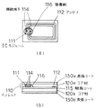
図6は、従来の非接触型ICカードの構造の一例を示す図であり、(a)は内部構造を示す図、(b)は断面図である。
【0006】
本従来例における非接触型ICカードは図6に示すように、樹脂シート115上に、外部からの情報の書き込み及び読み出しが可能なICモジュール111が搭載されるとともに、ICモジュール111の接続端子114を介してICモジュール111と接続され、外部に設けられた情報書込/読出装置(不図示)からの電磁誘導によりICモジュール111に電流を供給し、ICモジュール111に対する情報の書き込み及び読み出しを非接触状態にて行うための導電性のアンテナ112が形成されたインレット110が、コア材120a,120b及び表面シート130a,130bに挟まれるようにこれらが積層されて構成されている。なお、ICモジュール111は、接続端子114によってアンテナ112と接続された状態で、接着剤116によって樹脂シート115に接着されている。
【0007】
上記のように構成された非接触型ICカードにおいては、外部に設けられた情報書込/読出装置に近接させることにより、情報書込/読出装置からの電磁誘導によりアンテナ112からICモジュール111に電流が供給され、それにより、非接触状態において、情報書込/読出装置からICモジュール111に情報が書き込まれたり、ICモジュール111に書き込まれた情報が情報書込/読出装置にて読み出されたりする。
【0008】
以下に、上述した非接触型ICカードの製造方法について説明する。
【0009】
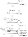
図7は、図6に示した非接触型ICカードの製造方法を説明するための図である。
【0010】
まず、樹脂シート115上に、エッチング、蒸着、もしくはシルク印刷等によってコイル形状のアンテナ112を形成する(図7(a))。
【0011】
次に、樹脂シート115上のICモジュール111が搭載される領域に、ディスペンサー等によるポッティング方式あるいはシルクスクリーン印刷方式等の方法によって接着剤116を滴下する(図7(b))。
【0012】
次に、樹脂シート115上の接着剤116が滴下された領域にICモジュール111を搭載し、ICモジュール111の接続端子114とアンテナ112とを接続し、その状態で、例えば、ICモジュール111に圧力をかけながら熱を加え、それにより、ICモジュール111と樹脂シート115とを接着剤116によって接着し、インレット110を完成させる(図7(c))。ここで、接着剤116としては、熱を加えることにより硬化する熱硬化型樹脂や、紫外線を照射することにより硬化する紫外線硬化型樹脂等が用いられる。熱硬化型樹脂を接着剤116として用いた場合は、ICモジュール111に圧力をかけながら熱を加え、それにより、接着剤116を硬化させ、また、紫外線硬化型樹脂を接着剤116として用いた場合は、ICモジュール111に圧力をかけながら紫外線を照射し、それにより、接着剤116を硬化させる。
【0013】
その後、インレット110を挟むように、コア材120a,120b及び表面シート130a,130bを積層し、これらを熱により圧着することにより非接触型ICカードを完成させる(図7(d))。なお、インレット110とコア材120a,120bと表面シート130a,130bとは、上述したように熱により圧着される場合に限らず、インレット110とコア材120a,120bとの間、並びに、コア材120a,120bと表面シート130a,130bとの間に接着層を設け、この接着層によって接着する場合もある。
【0014】
ここで、上述したような非接触型ICカードにおいては、携帯して使用される場合がほとんどであるため、折り曲げられる方向に外力が加わる可能性が高く、その場合、接着剤116が樹脂シート115から剥離し、それに伴い、ICモジュール111が樹脂シート115から剥離してICモジュール111とアンテナ112とが断線してしまう虞れがある。樹脂シート115は、接着力を高めるために易接着処理が施されているものの、表面の平坦性が優れているため、接着剤116と樹脂シート115との相性が良くない場合においては上述したような不具合が発生しやすくなってしまう。そのため、接着剤116として樹脂シート115に対して接着性の高いものを使用しなければならず、そのための手間がかかってしまったり、また、場合によってはコストアップが生じてしまう。
【0015】
そこで、図6に示したICモジュール111を弾性体材を介して樹脂シート115上に搭載し、それにより、非接触型ICカードに対して、折り曲げられる方向に外力が加わった場合において、ICモジュール111が樹脂シート115から剥離してしまう可能性を低減することが考えられている。
【0016】
図8は、従来の非接触型ICカードの構造の他の例を示す図であり、(a)は内部構造を示す図、(b)は断面図である。
【0017】
本従来例における非接触型ICカードは図8に示すように、樹脂シート215上に、外部からの情報の書き込み及び読み出しが可能なICモジュール211が弾性体材217を介して搭載されるとともに、ICモジュール211の接続端子214及び弾性体材217を介してICモジュール211と接続され、外部に設けられた情報書込/読出装置(不図示)からの電磁誘導によりICモジュール211に電流を供給し、ICモジュール211に対する情報の書き込み及び読み出しを非接触状態にて行うための導電性のアンテナ212が形成されたインレット210が、コア材220a,220b及び表面シート230a,230bに挟まれるようにこれらが積層されて構成されている。なお、ICモジュール211は、接続端子214及び弾性体材217を介してアンテナ212と接続された状態で、接着剤216によって樹脂シート215に接着されている。
【0018】
上記のように構成された非接触型ICカードにおいては、非接触型ICカードに対して、折り曲げられる方向に外力が加わった場合、その外力が弾性体材217によって吸収され、それにより、ICモジュール211が樹脂シート215から剥離してしまう可能性が低減されている(例えば、特許文献1参照)。
【0019】
また、その他に、樹脂シートに貫通穴を形成しておき、この貫通穴の接着剤が塗布された面とは反対側から接着剤を吸引し、それにより、接着剤を貫通穴に流し込み、接着剤とICモジュールとの接着力を高める技術も考えられている(例えば、特許文献2参照)。
【0020】
【特許文献1】
特開2000−200331号公報
【特許文献2】
特開平7−228084号公報
【0021】
【発明が解決しようとする課題】
しかしながら、上述したような従来の非接触型ICカードにおいては、弾性体材の分だけ非接触型ICカードの厚さが厚くなってしまうとともにコストアップが生じてしまうという問題点がある。
【0022】
ここで、非接触状態にて情報の書き込み及び読み出しが可能な記録媒体として、非接触型ICカードの他に、非接触型ICタグや非接触ICラベル、あるいは非接触型ICモジュールが内蔵されたはがき等が挙げられるが、これらはできるだけ薄いことが好ましく、厚さが厚くなってしまうことはできるだけ回避する必要がある。
【0023】
また、樹脂シートに貫通穴を形成しておき、この貫通穴の接着剤が塗布された面とは反対側から接着剤を吸引し、それにより、接着剤を貫通穴に流し込み、接着剤とICモジュールとの接着力を高めるものにおいては、接着剤を貫通穴に確実に吸引しながらも、ICモジュールを接着するために十分な量の接着剤をICモジュールが搭載される面に残す必要があるため、吸引力を精細に調整する必要が生じ、そのための手間やコストアップが生じてしまうという問題点がある。
【0024】
本発明は、上述したような従来の技術が有する問題点に鑑みてなされたものであって、RF−IDメディアの厚さを厚くすることなく、かつ、コストアップを生じさせることなく、RF−IDメディアに対して、折り曲げられる方向に外力が加わった場合にICモジュールがベース基材から剥離してしまう可能性を低減することができるRF−IDメディア及びその製造方法を提供することを目的とする。
【0025】
【課題を解決するための手段】
上記目的を達成するために本発明は、
ベース基材上に導電性を具備するアンテナが形成されるとともに、前記アンテナを介して非接触状態にて情報の書き込み及び読み出しが可能なICモジュールが、前記ベース基材上に供給された接着手段によって前記アンテナと電気的に接続された状態で前記ベース基材上に接着されて構成されたインレットを少なくとも有してなるRF−IDメディアにおいて、
前記ベース基材は、前記接着手段が供給される領域に複数の凹部を有することを特徴とする。
【0026】
また、前記凹部は、前記アンテナを避けるように、かつ、溝形状に形成されていることを特徴とする。
【0027】
また、前記凹部は、前記アンテナを避けるように、かつ、穴形状に形成されていることを特徴とする。
【0028】
また、前記凹部は、深さ方向が前記ベース基材の表面に対して斜めになるように形成されていることを特徴とする。
【0029】
また、前記凹部は、前記ベース基材を貫通するように形成されていることを特徴とする。
【0030】
また、前記RF−IDメディアの製造方法であって、
前記ベース基材上に前記アンテナを形成する工程と、
前記ベース基材上の前記接着手段が供給される領域に前記アンテナを避けるように前記凹部を形成する工程と、
前記ベース基材の前記ICモジュールが搭載される領域に前記接着手段を供給する工程と、
前記ベース基材上の前記接着手段が供給された領域に前記ICモジュールを搭載し、前記ICモジュールと前記アンテナとを電気的に接続する工程と、
前記ICモジュールと前記ベース基材とを前記接着手段によって接着する工程とを少なくとも有することを特徴とする。
【0031】
また、前記凹部は、レーザー光を照射することにより形成することを特徴とする。
【0032】
(作用)
上記のように構成された本発明においては、非接触状態にて情報の書き込み及び読み出しが可能なICモジュールが、ベース基材上に供給された接着手段によってベース基材上に接着されて構成されたインレットを少なくとも有してなるRF−IDメディアにおいて、ベース基材の接着手段が供給される領域に複数の凹部が形成されているので、ベース基材上に供給された接着手段がベース基材の凹部に入り込み、それにより、接着手段とベース基材との接触面積が大きくなるとともに、接着手段とベース基材との間にくさび効果が生じる。これにより、接着手段とベース基材との接着力が高まることになり、非接触型ICカードの厚さを厚くすることなく、かつ、コストアップを生じさせることなく、RF−IDメディアに対して、折り曲げられる方向に外力が加わった場合にICモジュールが接着手段とともにベース基材から剥離してしまう可能性が低減されることになる。
【0033】
また、この凹部が溝形状に形成されている場合は、接着手段とベース基材との間にて生じる気泡が溝に沿って逃げ易くなる。
【0034】
また、この凹部が、その深さ方向がベース基材の表面に対して斜めになるように形成されている場合は、RF−IDメディアに対して、折り曲げられる方向に外力が加わった場合に、接着手段がベース基材から剥がれようとする力に対する抵抗力が大きくなり、それにより、さらにICモジュールをベース基材から剥がれにくくすることができる。
【0035】
【発明の実施の形態】
以下に、本発明の実施の形態について図面を参照して説明する。
【0036】
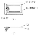
図1は、本発明のRF−IDメディアの実施の一形態である非接触型ICカードの構造の一例を示す図であり、(a)は内部構造を示す図、(b)は断面図であり、(c)はICモジュール11が搭載された領域の部分拡大図である。
【0037】
本形態は図1に示すように、ベース基材である樹脂シート15上に、外部からの情報の書き込み及び読み出しが可能なICモジュール11が搭載されるとともに、ICモジュール11の接続端子14を介してICモジュール11と接続され、外部に設けられた情報書込/読出装置(不図示)からの電磁誘導によりICモジュール11に電流を供給し、ICモジュール11に対する情報の書き込み及び読み出しを非接触状態にて行うための導電性のアンテナ12が形成されたインレット10が、コア材20a,20b及び表面シート30a,30bに挟まれるようにこれらが積層されて構成されている。なお、ICモジュール11は、接続端子14を介してアンテナ12と接続された状態で、接着剤16によって樹脂シート15に接着されている。また、樹脂シート15の接着剤16が供給される領域には、レーザー光を照射することにより形成された微細な凹部17が複数設けられている。
【0038】
上記のように構成された非接触型ICカードにおいては、外部に設けられた情報書込/読出装置に近接させることにより、情報書込/読出装置からの電磁誘導によりアンテナ12からICモジュール11に電流が供給され、それにより、非接触状態において、情報書込/読出装置からICモジュール11に情報が書き込まれたり、ICモジュール11に書き込まれた情報が情報書込/読出装置にて読み出されたりする。
【0039】
以下に、上述した非接触型ICカードの製造方法について説明する。
【0040】
図2は、図1に示した非接触型ICカードの製造方法を説明するための図である。
【0041】
まず、樹脂シート15上に、エッチング、蒸着、もしくはシルク印刷等によってコイル形状のアンテナ12を形成する(図2(a))。
【0042】
次に、樹脂シート15上の接着剤16が供給される領域において、アンテナ12を避けるようにレーザー光を照射し、複数の凹部17を形成する(図2(b))。
【0043】
次に、樹脂シート15上のICモジュール11が搭載される領域に、ディスペンサー等によるポッティング方式あるいはシルクスクリーン印刷方式等の方法によって接着剤16を滴下する(図2(c))。この際、樹脂シート15上に滴下された接着剤16は、樹脂シート15上に形成された凹部17の内部に入り込む。
【0044】
次に、樹脂シート15上の接着剤16が滴下された領域にICモジュール11を搭載し、ICモジュール11の接続端子14とアンテナ12とを接続し、その状態で、例えば、ICモジュール11に圧力をかけながら熱を加え、それにより、ICモジュール11と樹脂シート15とを接着し、インレット10を完成させる(図2(d))。ここで、接着剤16としては、熱を加えることにより硬化する熱硬化型樹脂や、紫外線を照射することにより硬化する紫外線硬化型樹脂等が用いられる。熱硬化型樹脂を接着剤16として用いた場合は、ICモジュール11に圧力をかけながら熱を加え、それにより、接着剤16を硬化させ、また、紫外線硬化型樹脂を接着剤16として用いた場合は、ICモジュール11に圧力をかけながら紫外線を照射し、それにより、接着剤16を硬化させる。
【0045】
その後、図2(d)に示したようなインレット10を挟むように、コア材20a,20b及び表面シート30a,30bを積層し、これらを熱により圧着することにより非接触型ICカードを完成させる(図2(e))。なお、インレット10とコア材20a,20bと表面シート30a,30bとは、上述したように熱により圧着される場合に限らず、インレット10とコア材20a,20bとの間、並びに、コア材20a,20bと表面シート30a,30bとの間に接着層を設け、この接着層によって接着することも考えられる。
【0046】
上述した工程によって製造された非接触型ICカードにおいては、ICモジュール11が搭載される樹脂シート15上に複数の凹部17が形成されており、この凹部17に、ICモジュール11と樹脂シート15とを接着する接着剤16が入り込んでいるため、接着剤16と樹脂シート15との接触面積が大きくなるとともに、接着剤16と樹脂シート15との間にくさび効果が生じ、それにより、接着剤16と樹脂シート15との接着力が高まる。これにより、非接触型ICカードの厚さを厚くすることなく、かつ、接着剤16の種類を限定したりすることによるコストアップを生じさせることなく、非接触型ICカードに対して、折り曲げられる方向に外力が加わった場合にICモジュール11が接着剤16とともに樹脂シート15から剥離してしまう可能性を低減することができる。
【0047】
以下に、樹脂シート15上に形成される凹部17の形状及びそれによる効果について説明する。
【0048】
図3は、図1に示した凹部17の形状の一例を説明するための図であり、(a)は樹脂シート15を表面から見た図、(b)は断面図である。
【0049】
本例における凹部17は図3(a)に示すように、樹脂シート15上の接着剤16が供給される領域において、アンテナ12に沿うような溝形状に形成されている。また、本例における凹部17は、樹脂シート15の表面に対して所定の角度を有するように斜め方向からレーザー光が照射されることによって形成されているため、図3(b)に示すように、その深さ方向が、樹脂シート15の表面に対して所定の角度を有して斜めになるように形成されている。
【0050】
図3に示すような凹部17が形成された非接触型ICカードにおいては、樹脂シート15の表面に対して所定の角度を有して斜めになるように凹部17が形成されているため、非接触型ICカードに対して、折り曲げられる方向に外力が加わった場合に、接着剤16が樹脂シート15から剥がれようとする力に対する抵抗力が大きくなり、それにより、さらにICモジュール11を樹脂シート15から剥がれにくくすることができる。
【0051】
また、凹部17が溝形状に形成されているため、接着剤16が樹脂シート15に供給された後にICモジュール11を搭載する際に接着剤16と樹脂シート15との間にて生じる気泡を溝に沿って逃し易くなる。
【0052】
図4は、図1に示した凹部17の形状の他の例を説明するための図であり、(a)は樹脂シート15を表面から見た図、(b)は断面図である。
【0053】
本例における凹部17は図4(a)に示すように、樹脂シート15上の接着剤16が供給される領域において、アンテナ12を避けるように複数の穴形状に形成されている。また、本例における凹部17は図4(b)に示すように、樹脂シート15を貫通するように形成されている。なお、この場合は、接着剤16が凹部17に入り込んだ際、凹部17に入り込んだ接着剤16が樹脂シート15の他方の面から流れ出ないように、接着剤16の粘度と凹部17の穴径とを設定する必要がある。
【0054】
図5は、図1に示した凹部17の形状の他の例を説明するための図である。
【0055】
本例における凹部17は図5に示すように、樹脂シート15上の接着剤16が供給される領域において、アンテナ12を避け、かつ、接着剤16のエッジにあたる領域に溝形状に形成されている。
【0056】
図5に示すような凹部17が形成された非接触型ICカードにおいては、接着剤16のエッジにあたる領域に凹部17が形成されているため、接着剤16のエッジ部分にて接着剤16と樹脂シート15とが強固に接着されることになり、それにより、非接触型ICカードに対して、折り曲げられる方向に外力が加わった場合に、さらにICモジュール11を樹脂シート15から剥がれにくくすることができる。
【0057】
なお、図3〜図5に示した凹部17の形状を組み合わせることも可能である。例えば、図3(a)に示したような溝形状の凹部17を、図4(b)に示すように樹脂シート15を貫通するように形成することや、図4(a)に示した複数の穴形状の凹部17を、図3(b)に示すようにその深さ方向が斜めになるように形成すること等が考えられる。また、図4(b)に示すように樹脂シート15を貫通するような凹部17を図3(b)に示すようにその深さ方向が斜めになるように形成することも考えられる。また、図3に示した溝形状のものと、図4に示した穴形状のものとを樹脂シート15上に組み合わせて形成することも考えられる。
【0058】
また、樹脂シート15上に形成される凹部17は、その面積が大きすぎる場合、コア材20a及び表面シート30aを積層した際に、表面シート30aの表面のうち凹部17が形成された領域においてくぼみが生じてしまうため、図3あるいは図5に示したような溝形状や、図4に示したような穴形状であることが好ましい。
【0059】
また、本形態においては、RF−IDメディアとして非接触状態にて情報の書き込み及び読み出しが可能な非接触型ICカードを例に挙げて説明したが、非接触型ICタグや非接触型ICラベル等も本発明を適用することができる。
【0060】
【発明の効果】
以上説明したように本発明においては、ベース基材上に導電性を具備するアンテナが形成されるとともに、アンテナを介して非接触状態にて情報の書き込み及び読み出しが可能なICモジュールが、ベース基材上に供給された接着手段によってアンテナと電気的に接続された状態でベース基材上に接着されて構成されたインレットを少なくとも有してなるRF−IDメディアにおいて、ベース基材が、接着手段が供給される領域に複数の凹部を有する構成としたため、ベース基材上に供給された接着手段がベース基材の凹部に入り込み、それにより、接着手段とベース基材との接着力を高めることができ、非接触型ICカードの厚さを厚くすることなく、かつ、コストアップを生じさせることなく、RF−IDメディアに対して、折り曲げられる方向に外力が加わった場合にICモジュールが接着手段とともにベース基材から剥離してしまう可能性を低減することができる。
【0061】
また、この凹部が溝形状に形成されているものにおいては、接着手段とベース基材との間にて生じる気泡を溝に沿って逃げ易くすることができる。
【0062】
また、この凹部が、その深さ方向がベース基材の表面に対して斜めになるように形成されているものにおいては、RF−IDメディアに対して、折り曲げられる方向に外力が加わった場合に、接着手段がベース基材から剥がれようとする力に対する抵抗力が大きくなり、それにより、さらにICモジュールをベース基材から剥がれにくくすることができる。
【図面の簡単な説明】
【図1】本発明のRF−IDメディアの実施の一形態である非接触型ICカードの構造の一例を示す図であり、(a)は内部構造を示す図、(b)は断面図であり、(c)はICモジュールが搭載された領域の部分拡大図である。
【図2】図1に示した非接触型ICカードの製造方法を説明するための図である。
【図3】図1に示した凹部の形状の一例を説明するための図であり、(a)は樹脂シートを表面から見た図、(b)は断面図である。
【図4】図1に示した凹部の形状の他の例を説明するための図であり、(a)は樹脂シートを表面から見た図、(b)は断面図である。
【図5】図1に示した凹部の形状の他の例を説明するための図である。
【図6】従来の非接触型ICカードの構造の一例を示す図であり、(a)は内部構造を示す図、(b)は断面図である。
【図7】図6に示した非接触型ICカードの製造方法を説明するための図である。
【図8】従来の非接触型ICカードの構造の他の例を示す図であり、(a)は内部構造を示す図、(b)は断面図である。
【符号の説明】
10 インレット
11 ICモジュール
12 アンテナ
14 接続端子
15 樹脂シート
16 接着剤
17 凹部
20a,20b コア材
30a,30b 表面シート[0001]
TECHNICAL FIELD OF THE INVENTION
The present invention relates to an RF-ID medium capable of writing and reading information in a non-contact state, and a method for manufacturing the same.
[0002]
[Prior art]
In recent years, with the progress of the information society, information is recorded on a card, and information management, settlement, and the like using the card are performed.
[0003]
Cards used for such information management and settlement include IC cards with built-in IC chips and magnetic cards on which information is written by magnetism. Information can be written and read using a dedicated device. Is
[0004]
Further, in the IC card, a contact type IC card which performs writing and reading of information by contacting with a dedicated device, and a non-contact type IC which can perform writing and reading of information only by approaching the dedicated device. There is a card. These IC cards have higher security and a larger amount of writable information than magnetic cards, and one card can be used for a variety of purposes, so that its popularity in the market is ever increasing. . Among them, a non-contact type IC card is convenient for handling because it is not necessary to take out the card and insert it into a dedicated device when writing or reading information. The device for reading the information is rapidly spreading.
[0005]
6A and 6B are diagrams showing an example of the structure of a conventional non-contact type IC card, wherein FIG. 6A is a diagram showing an internal structure, and FIG. 6B is a sectional view.
[0006]
As shown in FIG. 6, the non-contact type IC card according to this conventional example has an
[0007]
In the non-contact type IC card configured as described above, the
[0008]
Hereinafter, a method for manufacturing the above-mentioned non-contact type IC card will be described.
[0009]
FIG. 7 is a view for explaining a method of manufacturing the non-contact type IC card shown in FIG.
[0010]
First, the coil-
[0011]
Next, an
[0012]
Next, the
[0013]
Thereafter, the core members 120a, 120b and the
[0014]
Here, in the non-contact type IC card as described above, since it is almost always carried and used, there is a high possibility that an external force will be applied in the direction in which the IC card is bent. From the
[0015]
Therefore, the
[0016]
8A and 8B are diagrams showing another example of the structure of the conventional non-contact type IC card, wherein FIG. 8A is a diagram showing the internal structure, and FIG. 8B is a sectional view.
[0017]
As shown in FIG. 8, the non-contact type IC card in this conventional example has an
[0018]
In the non-contact type IC card configured as described above, when an external force is applied to the non-contact type IC card in a bending direction, the external force is absorbed by the
[0019]
In addition, a through-hole is formed in the resin sheet, and the adhesive is sucked from the side opposite to the surface of the through-hole on which the adhesive is applied, so that the adhesive flows into the through-hole and is bonded. A technique for increasing the adhesive strength between the agent and the IC module has also been considered (for example, see Patent Document 2).
[0020]
[Patent Document 1]
JP 2000-200331 A [Patent Document 2]
Japanese Patent Application Laid-Open No. 7-228084
[Problems to be solved by the invention]
However, in the conventional non-contact type IC card as described above, there is a problem that the thickness of the non-contact type IC card is increased by the amount of the elastic material and the cost is increased.
[0022]
Here, in addition to a non-contact type IC card, a non-contact type IC tag, a non-contact type IC label, or a non-contact type IC module is incorporated as a recording medium on which information can be written and read in a non-contact state. Postcards and the like are mentioned, but it is preferable that these are as thin as possible, and it is necessary to avoid thickening as much as possible.
[0023]
Further, a through hole is formed in the resin sheet, and the adhesive is sucked from the side opposite to the surface on which the adhesive of the through hole is applied, whereby the adhesive flows into the through hole, and the adhesive and the IC In the case of enhancing the adhesive strength to the module, it is necessary to leave a sufficient amount of adhesive on the surface on which the IC module is mounted, while securely sucking the adhesive into the through hole, while adhering the IC module. Therefore, it is necessary to finely adjust the suction force, and there is a problem that labor and cost increase for the adjustment.
[0024]
The present invention has been made in view of the above-mentioned problems of the conventional technology, and has been made without increasing the thickness of the RF-ID medium and without increasing the cost. An object of the present invention is to provide an RF-ID medium and a method for manufacturing the same, which can reduce the possibility that the IC module will peel off from the base material when an external force is applied to the ID medium in a direction in which the medium is bent. I do.
[0025]
[Means for Solving the Problems]
In order to achieve the above object, the present invention provides
An antenna having conductivity is formed on a base material, and an IC module capable of writing and reading information in a non-contact state via the antenna is provided on the base material by bonding means. In an RF-ID medium having at least an inlet configured to be adhered to the base material in a state of being electrically connected to the antenna,
The base substrate has a plurality of recesses in a region where the bonding unit is supplied.
[0026]
Further, the recess is formed so as to avoid the antenna and has a groove shape.
[0027]
Further, the recess is formed so as to avoid the antenna and has a hole shape.
[0028]
Further, the concave portion is formed so that a depth direction is oblique to a surface of the base substrate.
[0029]
Further, the recess is formed so as to penetrate the base substrate.
[0030]
Also, the method for manufacturing the RF-ID media,
Forming the antenna on the base substrate,
Forming the concave portion so as to avoid the antenna in an area on the base material where the bonding means is supplied,
Supplying the bonding means to an area of the base material on which the IC module is mounted;
A step of mounting the IC module in an area on the base substrate to which the bonding unit is supplied, and electrically connecting the IC module and the antenna;
And a step of bonding the IC module and the base substrate by the bonding means.
[0031]
Further, the recess is formed by irradiating a laser beam.
[0032]
(Action)
In the present invention configured as described above, the IC module capable of writing and reading information in a non-contact state is configured to be bonded to the base substrate by the bonding unit supplied on the base substrate. In the RF-ID media having at least the inlet, the plurality of recesses are formed in the region of the base material to which the bonding means are supplied, so that the bonding means supplied on the base material is , The contact area between the bonding means and the base material is increased, and a wedge effect is generated between the bonding means and the base material. As a result, the adhesive force between the bonding means and the base material is increased, so that the thickness of the non-contact type IC card is not increased, and the cost is not increased. In addition, when an external force is applied in the direction in which the IC module is bent, the possibility that the IC module is peeled off from the base substrate together with the bonding means is reduced.
[0033]
In addition, when the concave portion is formed in a groove shape, bubbles generated between the bonding means and the base material can easily escape along the groove.
[0034]
Further, when the concave portion is formed so that its depth direction is oblique to the surface of the base material, when an external force is applied to the RF-ID medium in a direction in which the RF-ID medium is bent, The resistance of the bonding means to the force of peeling off from the base substrate is increased, thereby making it more difficult for the IC module to peel off from the base substrate.
[0035]
BEST MODE FOR CARRYING OUT THE INVENTION
Hereinafter, embodiments of the present invention will be described with reference to the drawings.
[0036]
FIG. 1 is a view showing an example of the structure of a non-contact type IC card which is an embodiment of the RF-ID medium of the present invention, (a) showing an internal structure, and (b) a sectional view. FIG. 3C is a partially enlarged view of a region where the
[0037]
In this embodiment, as shown in FIG. 1, an
[0038]
In the non-contact type IC card configured as described above, the
[0039]
Hereinafter, a method for manufacturing the above-mentioned non-contact type IC card will be described.
[0040]
FIG. 2 is a diagram for explaining a method of manufacturing the non-contact type IC card shown in FIG.
[0041]
First, the coil-shaped
[0042]
Next, in a region where the adhesive 16 is supplied on the
[0043]
Next, an adhesive 16 is dropped onto a region of the
[0044]
Next, the
[0045]
Thereafter, the core members 20a and 20b and the
[0046]
In the non-contact type IC card manufactured by the above-described process, a plurality of
[0047]
Hereinafter, the shape of the
[0048]
3A and 3B are diagrams for explaining an example of the shape of the
[0049]
As shown in FIG. 3A, the
[0050]
In the non-contact type IC card in which the
[0051]
Further, since the
[0052]
4A and 4B are diagrams for explaining another example of the shape of the
[0053]
As shown in FIG. 4A, the
[0054]
FIG. 5 is a view for explaining another example of the shape of the
[0055]
As shown in FIG. 5, the
[0056]
In the non-contact type IC card in which the
[0057]
It is also possible to combine the shapes of the
[0058]
If the area of the
[0059]
In this embodiment, a non-contact IC card capable of writing and reading information in a non-contact state as an RF-ID medium has been described as an example, but a non-contact IC tag and a non-contact IC label are described. Etc. can also apply the present invention.
[0060]
【The invention's effect】
As described above, in the present invention, an IC module in which a conductive antenna is formed on a base substrate and in which information can be written and read in a non-contact state via the antenna is provided. In an RF-ID medium having at least an inlet configured to be adhered to a base material in a state where the base material is electrically connected to the antenna by a bonding means supplied on the material, the base material may be bonded to the antenna. Is provided with a plurality of recesses in the area where the base material is supplied, so that the bonding means supplied on the base material enters the recesses of the base material, thereby increasing the adhesive force between the bonding means and the base material. Without bending the RF-ID media without increasing the thickness of the non-contact type IC card and without increasing the cost. IC module can be reduced possibly be peeled from the base material together with the adhesive means when an external force is applied to that direction.
[0061]
In the case where the concave portion is formed in a groove shape, air bubbles generated between the bonding means and the base material can be easily escaped along the groove.
[0062]
Further, in the case where the concave portion is formed so that its depth direction is oblique to the surface of the base material, when an external force is applied to the RF-ID medium in a direction in which the medium is bent. In addition, the resistance of the bonding means to the force of peeling off from the base material is increased, thereby further preventing the IC module from being peeled off from the base material.
[Brief description of the drawings]
FIG. 1 is a diagram showing an example of the structure of a non-contact type IC card which is an embodiment of the RF-ID medium of the present invention, (a) showing an internal structure, and (b) a sectional view. FIG. 2C is a partially enlarged view of an area where an IC module is mounted.
FIG. 2 is a view for explaining a method of manufacturing the non-contact type IC card shown in FIG.
3A and 3B are views for explaining an example of the shape of a concave portion shown in FIG. 1, wherein FIG. 3A is a view of a resin sheet viewed from the surface, and FIG. 3B is a cross-sectional view.
4A and 4B are views for explaining another example of the shape of the concave portion shown in FIG. 1, wherein FIG. 4A is a view of the resin sheet viewed from the surface, and FIG. 4B is a cross-sectional view.
FIG. 5 is a view for explaining another example of the shape of the recess shown in FIG. 1;
6A and 6B are diagrams showing an example of the structure of a conventional non-contact type IC card, wherein FIG. 6A is a diagram showing an internal structure, and FIG. 6B is a sectional view.
FIG. 7 is a diagram for explaining a method of manufacturing the non-contact type IC card shown in FIG.
8A and 8B are diagrams showing another example of the structure of a conventional non-contact type IC card, wherein FIG. 8A is a diagram showing an internal structure, and FIG. 8B is a sectional view.
[Explanation of symbols]
Claims (7)
前記ベース基材は、前記接着手段が供給される領域に複数の凹部を有することを特徴とするRF−IDメディア。An antenna having conductivity is formed on a base material, and an IC module capable of writing and reading information in a non-contact state via the antenna is provided on the base material by bonding means. In an RF-ID medium having at least an inlet configured to be adhered to the base material in a state of being electrically connected to the antenna,
The RF-ID medium, wherein the base material has a plurality of concave portions in a region where the bonding unit is supplied.
前記凹部は、前記アンテナを避けるように、かつ、溝形状に形成されていることを特徴とするRF−IDメディア。The RF-ID medium according to claim 1,
The recess is formed in a groove shape so as to avoid the antenna and is formed in a groove shape.
前記凹部は、前記アンテナを避けるように、かつ、穴形状に形成されていることを特徴とするRF−IDメディア。The RF-ID medium according to claim 1,
The recess is formed in a hole shape so as to avoid the antenna and is formed in a hole shape.
前記凹部は、深さ方向が前記ベース基材の表面に対して斜めになるように形成されていることを特徴とするRF−IDメディア。The RF-ID medium according to any one of claims 1 to 3,
The concave portion is formed so that a depth direction is oblique to a surface of the base substrate.
前記凹部は、前記ベース基材を貫通するように形成されていることを特徴とするRF−IDメディア。The RF-ID medium according to any one of claims 1 to 4,
The concave portion is formed so as to penetrate the base material.
前記ベース基材上に前記アンテナを形成する工程と、
前記ベース基材上の前記接着手段が供給される領域に前記アンテナを避けるように前記凹部を形成する工程と、
前記ベース基材の前記ICモジュールが搭載される領域に前記接着手段を供給する工程と、
前記ベース基材上の前記接着手段が供給された領域に前記ICモジュールを搭載し、前記ICモジュールと前記アンテナとを電気的に接続する工程と、
前記ICモジュールと前記ベース基材とを前記接着手段によって接着する工程とを少なくとも有することを特徴とするRF−IDメディアの製造方法。It is a manufacturing method of the RF-ID media as described in any one of Claims 1 thru | or 5, Comprising:
Forming the antenna on the base substrate,
Forming the concave portion so as to avoid the antenna in an area on the base material where the bonding means is supplied,
Supplying the bonding means to an area of the base material on which the IC module is mounted;
A step of mounting the IC module in an area on the base substrate to which the bonding unit is supplied, and electrically connecting the IC module and the antenna;
Bonding the IC module and the base substrate by the bonding unit.
前記凹部は、レーザー光を照射することにより形成することを特徴とするRF−IDメディアの製造方法。The method for manufacturing an RF-ID medium according to claim 6,
The method of manufacturing an RF-ID medium, wherein the recess is formed by irradiating a laser beam.
Priority Applications (1)
| Application Number | Priority Date | Filing Date | Title |
|---|---|---|---|
| JP2002268503A JP2004110141A (en) | 2002-09-13 | 2002-09-13 | Rf-id media and its manufacturing method |
Applications Claiming Priority (1)
| Application Number | Priority Date | Filing Date | Title |
|---|---|---|---|
| JP2002268503A JP2004110141A (en) | 2002-09-13 | 2002-09-13 | Rf-id media and its manufacturing method |
Publications (1)
| Publication Number | Publication Date |
|---|---|
| JP2004110141A true JP2004110141A (en) | 2004-04-08 |
Family
ID=32266702
Family Applications (1)
| Application Number | Title | Priority Date | Filing Date |
|---|---|---|---|
| JP2002268503A Pending JP2004110141A (en) | 2002-09-13 | 2002-09-13 | Rf-id media and its manufacturing method |
Country Status (1)
| Country | Link |
|---|---|
| JP (1) | JP2004110141A (en) |
Cited By (3)
| Publication number | Priority date | Publication date | Assignee | Title |
|---|---|---|---|---|
| JP2011061054A (en) * | 2009-09-11 | 2011-03-24 | Toppan Forms Co Ltd | Electronic circuit board |
| US8081081B2 (en) | 2007-11-21 | 2011-12-20 | Fujitsu Limited | Electronic apparatus and method of manufacturing the same |
| JP2017117468A (en) * | 2015-12-22 | 2017-06-29 | デクセリアルズ株式会社 | IC card |
-
2002
- 2002-09-13 JP JP2002268503A patent/JP2004110141A/en active Pending
Cited By (4)
| Publication number | Priority date | Publication date | Assignee | Title |
|---|---|---|---|---|
| US8081081B2 (en) | 2007-11-21 | 2011-12-20 | Fujitsu Limited | Electronic apparatus and method of manufacturing the same |
| JP2011061054A (en) * | 2009-09-11 | 2011-03-24 | Toppan Forms Co Ltd | Electronic circuit board |
| JP2017117468A (en) * | 2015-12-22 | 2017-06-29 | デクセリアルズ株式会社 | IC card |
| JP7005138B2 (en) | 2015-12-22 | 2022-01-21 | デクセリアルズ株式会社 | IC card |
Similar Documents
| Publication | Publication Date | Title |
|---|---|---|
| US8162231B2 (en) | Noncontact IC tag label and method of manufacturing the same | |
| US20110011939A1 (en) | Contact-less and dual interface inlays and methods for producing the same | |
| JP4241147B2 (en) | IC card manufacturing method | |
| JP2007042087A (en) | Rfid tag and production method therefor | |
| TWI284842B (en) | Communication medium capable of carrying out contactless communication and method of producing the same | |
| JPH11345302A (en) | Mounting method for ic chip, ic module, inlet and ic card | |
| JP2006155571A (en) | Ic tag | |
| JP2004110141A (en) | Rf-id media and its manufacturing method | |
| JP5049025B2 (en) | Non-contact IC tag | |
| JP2003288568A (en) | Contactless ic label | |
| JP4306352B2 (en) | Contact type non-contact type hybrid IC module and contact type non-contact type hybrid IC card using the same | |
| KR101014154B1 (en) | Flip chip mounting substrate | |
| JP4848214B2 (en) | Non-contact IC tag | |
| JP2003132322A (en) | Combination type ic card and its manufacturing method | |
| JPH11134458A (en) | Ic card | |
| JP2004110142A (en) | Recording medium | |
| JP2015108933A (en) | Noncontact ic card | |
| JP2004334639A (en) | Ic card and manufacturing method thereof | |
| JP3936217B2 (en) | RF-ID media and manufacturing method thereof | |
| JP2008046910A (en) | Method for manufacturing semiconductor device | |
| JP2004280392A (en) | Method for manufacturing information recording medium | |
| JP4085790B2 (en) | IC card manufacturing method | |
| JP2004355337A (en) | Rf-id medium, its manufacturing method, and information writing/reading device | |
| JP4236972B2 (en) | Combination type IC card and manufacturing method thereof | |
| JP4040341B2 (en) | Method for manufacturing RF-ID media |
Legal Events
| Date | Code | Title | Description |
|---|---|---|---|
| A621 | Written request for application examination |
Free format text: JAPANESE INTERMEDIATE CODE: A621 Effective date: 20050825 |
|
| RD03 | Notification of appointment of power of attorney |
Free format text: JAPANESE INTERMEDIATE CODE: A7423 Effective date: 20050825 |
|
| A977 | Report on retrieval |
Free format text: JAPANESE INTERMEDIATE CODE: A971007 Effective date: 20070830 |
|
| A131 | Notification of reasons for refusal |
Free format text: JAPANESE INTERMEDIATE CODE: A131 Effective date: 20070919 |
|
| A02 | Decision of refusal |
Free format text: JAPANESE INTERMEDIATE CODE: A02 Effective date: 20080206 |