【0001】
【発明の属する技術分野】
本発明は、チップ型固体電解コンデンサに関し、より詳しくは、コンデンサ素子と接続ランドの接続の信頼性を向上させたチップ型固体電解コンデンサに関する。
【0002】
【従来の技術】
図12は、従来のチップ型固体電解コンデンサの一部を切り開いて示す斜視図であり、図13は、図12のA−A線に沿った断面図である。図12と図13を参照して従来のチップ型固体電解コンデンサについて説明する。
【0003】
従来のチップ型固体電解コンデンサは、例えば特開2002−134362号公報に示されているように、[1]絶縁板21の上面に陽極接続ランド7と陰極接続ランド8を備え、その下面に前記ランドと絶縁板21に設けられた陽極スルーホール9および陰極スルーホール10のそれぞれを介して接続されている陽極端子4および陰極端子5を備えたプリント回路板(以下、PWBと呼称することがある)14と、[2]前記陽極接続ランド7の表面に植立された導電材12と、[3]一側面に陽極リード線2が植立され、他の面に陰極層(図示していない)が形成され、陽極リード線2が導電材12に接続され、該陰極層が導電性接着剤3を介して陰極接続ランド8に接続されて、PWB14の上面に搭載されたコンデンサ素子1と、[4]PWB14の上面のコンデンサ素子1を外装した外装樹脂6とを具備している。
【0004】
【発明が解決しようとする課題】
上記の従来のチップ型固体電解コンデンサには、PWB14の平面状の陽極接続ランド7に導電材12を導電性接着剤またははんだを介して植立し、陰極接続ランド8にコンデンサ素子1の陰極層を導電性接着剤3にて接着し、外装樹脂6にて外装を行っているために、実装時の熱ストレスや機械的ストレスにより、陽極接続ランド7と導電材12の間や陰極接続ランド8と導電性接着剤3の間およびPWB14と外装樹脂6の間に剥離が発生し、オープン不良が発生するという問題点があった。
【0005】
本発明の目的は、上記の従来技術の問題点を解決し、陽極端子および陰極端子のフレキシビリティと寸法精度の向上と大きなコンデンサ素子領域が確保されたチップ型固体電解コンデンサを提供することにある。
【0006】
このことは、外部端子の接続信頼性にすぐれ、外形サイズが縮小でき、大容量化が可能なチップ型固体電解コンデンサを提供することであると言い換えてもよい。
【0007】
【課題を解決するための手段】
本発明の第1の構成のチップ型固体電解コンデンサは、絶縁板の上面に、第1のランド、および、格子状またはストライプ状にエッチングを施した第2のランドを備え、前記絶縁板の下面に前記第1および第2のランドにそれぞれ電気接続用のスルーホールを介して接続された第1の端子および第2の端子を備え、前記ランドとは重ならない絶縁板の位置に固定用のスルーホールが設けられたプリント回路板と、前記第1のランド表面に植立された導電材と、外表面に陽極リード線および陰極層が設けられ、前記陽極リード線が前記導電材に溶接にて接続され、前記陰極層が導電性接着剤を介して前記第2のランドに接続されて、前記プリント回路板の上面に搭載されたコンデンサ素子と、前記コンデンサ素子を含む前記プリント回路板の上全面を外装する外装樹脂とを具備することを特徴とする。
【0008】
上記本発明の第1の構成において、前記コンデンサ素子は2個以上並列に接続されて前記プリント回路板の上面に配置されてもよい。
【009】
また、前記第1のランドと前記導電材がレーザ溶接によって接続されているとよい。
【0010】
また、前記絶縁板の下面に、前記第1および第2の端子に加えて、第3および第4の端子が設けられ、前記第1のないし第4の端子の4つの位置は、ほぼ4角形を構成して、前記ほぼ4角形の対角線上の2つの端子が同極となるように、前記プリント基板の電気接続用のスルーホールに加えて内部配線および電気接続用のバイアホールを設けて接続された4端子を具備するとよい。
【0011】
本発明の第2の構成のチップ型固体電解コンデンサは、絶縁板の上面に設けられた第1のランドおよび第2のランドを備え、前記絶縁板の下面に前記第1および第2のランドにそれぞれ電気接続用のスルーホールを介して接続された第1の端子および第2の端子を備え、前記ランドとは重ならない絶縁板の位置に固定用のスルーホールが設けられたプリント回路板と、前記第1のランド表面に植立された導電材と、外表面に陽極リード線および陰極層が設けられ、前記陽極リード線が前記導電材に接続され、前記陰極層が前記第2のランドに張り付けた導電性テープと導電性接着剤を介して前記第2のランドに接続されて、前記プリント回路板の上面に搭載されたコンデンサ素子と、前記コンデンサ素子を含む前記プリント回路板の上全面を外装する外装樹脂とを具備することを特徴とする。
【0012】
上記本発明の第2の構成において、前記コンデンサ素子は2個以上並列に接続されて前記プリント回路板の上面に配置されてもよい。
【0013】
また、前記第1のランドと前記導電材が溶接によって接続されているとよい。
【0014】
また、前記絶縁板の下面に、前記第1および第2の端子に加えて、第3および第4の端子が設けられ、前記第1のないし第4の端子の4つの位置は、ほぼ4角形を構成して、前記ほぼ4角形の対角線上の2つの端子が同極となるように、前記プリント基板における電気接続用のスルーホールに加えて内部配線および電気接続用のバイアホールを設けて接続された4端子を具備するとよい。
【0015】
本発明の第3の構成のチップ型固体電解コンデンサは、絶縁板の上面に、第1のランド、および、固定用のバイアホールを有する第2のランドを備え、前記絶縁板の下面に前記ランドのそれぞれに電気接続用のスルーホールを介して接続された第1の端子および第2の端子を備え、前記第1のランドと前記第2のランドの間に設けられ内部配線とは独立した固定用のバイアホール、および第2のランドに設けられた固定用のバイアホールを備えたプリント回路板と、前記第1のランド表面に植立された導電材と、外表面に陽極リード線および陰極層が設けられ、前記陽極リード線が前記導電材に溶接にて接続され、前記陰極層が導電性接着剤を介して前記第2のランドに接続されて、前記プリント回路板の上面に搭載されたコンデンサ素子と、前記コンデンサ素子を含む前記プリント回路板の上全面を外装する外装樹脂とを具備することを特徴とする。
【0016】
上記本発明の第3の構成において、前記コンデンサ素子は2個以上並列に接続されて前記プリント回路板の上面に配置されてもよい。
【0017】
また、前記第1のランドと前記導電材がレーザ溶接によって接続されているとよい。
【0018】
また、前記絶縁板の下面に、前記第1および第2の端子に加えて、第3および第4の端子が設けられ、前記第1のないし第4の端子の4つの位置は、ほぼ4角形を構成して、前記ほぼ4角形の対角線上の2つの端子が、同極となるように、前記プリント基板における電気接続用のスルーホールに加えて内部配線および電気接続用のバイアホールを設けて接続された4端子を具備するとよい。
【0019】
上記本発明の1、2または3の構成のチップ型固体電解コンデンサにおいて、前記4端子の表面に、はんだボールを設け、BGA(ボール・グリッド・アレイ)型の固体電解コンデンサにするとよい。
【0020】
上記本発明の1、2または3の構成のチップ型固体電解コンデンサにおいて、前記導電材は銅、銅合金または鉄ニッケル合金であるとよい。
【0021】
【発明の実施の形態】
次に、本発明の実施の形態について図面を参照して詳細に説明する。
【0022】
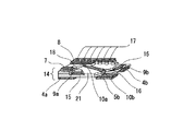
(実施の形態1)図1は、本発明の第1の実施の形態におけるチップ型固体電解コンデンサの一部を切り開いて示す斜視図であり、図2は、図1のA−A線に沿った断面図である。なお、図1において、外装樹脂の他にコンデンサ素子および陰極接続部付近が部分的に除去されている。
【0023】
図1、図2において、図12、図13に示した従来例の部分と同等の部分には同じ参照番号が付せられているので重複する説明は省略する。
【0024】
本実施の形態1のチップ型固体電解コンデンサは、[1]絶縁板21の上面に陽極接続ランド7と格子状にエッチングを施した陰極接続ランド8を備え、その下面に該各ランドと絶縁板21を通して設けられた陽極スルーホール9および陰極スルーホール10のそれぞれを介して接続されている陽極端子4および陰極端子5を備え、陽極接続ランド7および陰極接続ランド8と重ならない絶縁板の位置に固定用スルーホール11を設けたPWB14と、[2]陽極接続ランド7の表面にレーザ溶接によって植立された導電材12と、[3]一方の側面に陽極リード線2が植立され、他の面に陰極層(表示していない)が形成され、前記陽極リード線2を導電材12を介して陽極接続ランド7に接続し、前記陰極層が導電性接着剤3を介して陰極接続ランド8に接続されてPWB14の上面に搭載されたコンデンサ素子1と、[4]PWB14の上面のコンデンサ素子1を外装した外装樹脂6とを備えている。
【0025】
ここで、陽極接続ランド7と導電材12の接続はレーザ溶接によって行われており、本チップ型固体電解コンデンサの実装時のはんだ付け温度による陽極接続ランド7と導電材12の接続信頼性の低下を防止している。
【0026】
PWB14の絶縁板21の材料には厚さ0.1〜0.3mmのエポキシ樹脂、ポリイミド樹脂、フッ素樹脂等が使用できる。またPWB14の陽極接続ランド7、陰極接続ランド8、陽極端子4および陰極端子5、並びに陽極スルーホール9および陰極スルーホール10には銅金属膜が用いられ、表面にNiめっきとAuめっきを施すことができる。なお、PWB14は通常のプリント配線技術によって製造できる。
【0027】
また、導電材12の材料には、銅(Cu)、銅合金または鉄ニッケル(Fe−Ni)合金が使用できる。
【0028】
コンデンサ素子1は、陽極リード線2を植立したタンタル金属からなる陽極体に、公知の手段で順次、誘電体層、固体電解質層、陰極層が形成されている。外装樹脂6にはエポキシ樹脂が使用され、トランスファーモールド成型によってPWB14の上面に形成される。
【0029】
次に、図1、図2を参照して本実施の形態1のチップ型固体電解コンデンサの製造方法を説明する。
【0030】
まず、エポキシ樹脂製の両面銅張り絶縁板21に穴あけした後、銅めっきとエッチングにより絶縁板21の両面に矩形状の陽極接続ランド7、格子状の陰極接続ランド8、陽極端子4、陰極端子5、両面の各ランドと各端子を接続する陽極スルーホール9および陰極スルーホール10を形成し、陽極接続ランド7および陰極接続ランド8とは回路的に重ならない独立した位置に固定用スルーホール11を形成してPWB14を製造する。
【0031】
両面銅張り絶縁板の銅箔の厚さは5〜18μm、銅めっきは電気めっき銅または無電解銅めっきで10〜25μmの厚さに形成される。また、絶縁板21に穴あけされる穴径(直径)は0.25〜5mmである。
【0032】
次に、陽極接続ランド7の表面に銅(Cu)、銅合金または鉄ニッケル(Fe−Ni)合金からなる導電材12をレーザ溶接にて接続する。
【0033】
次に、公知の技術によりタンタル金属からなる陽極体に陽極リード線2を植立し、この陽極体に、順次、誘電体層、固体電解質層、陰極層を形成することによって形成されたコンデンサ素子1を準備する。
【0034】
このコンデンサ素子をPWB14の上面に配置する。陰極層がPWB14の陰極接続ランド上に、陽極リード線2が導電材12上に来るように位置調整し、コンデンサ素子1の陰極層を銀、銅、ニッケル等を含む導電性接着剤3を介してPWB14の陰極接続ランド8に接続する。
【0035】
次に、陽極リード線2を導電材12に溶接した後、PWB14の上全体をエポキシ樹脂を使用してトランスファーモールド法によって樹脂外装し、チップ型固体電解コンデンサが完成する。
【0036】
なお、大きなサイズの絶縁板を使用して、この絶縁板に複数個のPWB14を形成し、この複数個のPWB14の上面に複数個のコンデンサ素子1を実装してトランスファーモールド法によって樹脂外装後、切断加工によって個別のチップ型固体電解コンデンサに分離してもよい。
【0037】
上記本発明の実施の形態1によるチップ型固体電解コンデンサは、格子状の陰極接続ランド8のエッチング部に導電性接着剤3が入り込み、また、スルーホール11には外装樹脂6が入り込み、それぞれのアンカー効果によって剥離を防止して、オープン不良の発生を防止できる。
【0038】
また、格子状にエッチングした陰極接続ランドに換えて、電気的導通が確保されていれば、ストライプ状にエッチングされた陰極接続ランドを用いてもよい。
【0039】
(実施の形態2)次に、本発明の第2の実施の形態におけるチップ型固体電解コンデンサについて説明する。図3は、本発明の第2の実施の形態におけるチップ型固体電解コンデンサの一部を切り開いて示す斜視図であり、図4は、図3のA−A線に沿った断面図である。なお、図3において、外装樹脂の他にコンデンサ素子および陰極接続部付近が部分的に除去されている。
【0040】
本実施の形態2では、上記実施の形態1のチップ型固体電解コンデンサに対して、陰極接続ランド8を格子状にエッチングを施した形状とする代わりに、矩形状として、この陰極接続ランド8上に導電性テープ13を張り付け、導電性接着剤3を介してコンデンサ素子1の陰極層を陰極接続ランド8に接続してPWB14の上面にコンデンサ素子1を搭載して、外装樹脂6にて外装することを特徴としている。
【0041】
この実施の形態2のチップ型固体電解コンデンサは、導電性接着剤3を介してコンデンサ素子1の陰極層を陰極接続ランド8に接続した際に、導電性接着剤3が硬化するまでの工程中のコンデンサ素子1の位置ずれを導電性テープ13により防止し、硬化後も導電性テープ13の切込みによる導電性接着剤3とのアンカー効果によって剥離を防止して、オープン不良の発生率を改善できる。
【0042】
なお、本実施の形態のチップ型固体電解コンデンサは、導電性テープ13を張り付ける以外はPWB14の製造から、コンデンサ素子1をこのPWB14に実装するまで、上記の実施の形態1と同様な工程によって行われる。
【0043】
(実施の形態3)次に、本発明の第3の実施の形態におけるチップ型固体電解コンデンサについて説明する。図5は、本発明の第3の実施の形態におけるチップ型固体電解コンデンサの一部を切り開いて示す斜視図であり、図6は、図5のA−A線に沿った断面図である。なお、図5において、外装樹脂の他にコンデンサ素子および陰極接続部付近が部分的に除去されている。
【0044】
本実施の形態では、上記本発明の実施の形態1におけるチップ型固体電解コンデンサに対して、陰極接続ランド8に固定用陰極バイアホール17を複数個施した矩形状とし、陽極接続ランド7とランドと陰極接続ランド8の間に内部配線とは独立した固定用バイアホール18を備えたことを特徴としている。
【0045】
この実施の形態3におけるチップ型固体電解コンデンサは、上記実施の形態1のチップ型固体電解コンデンサに対して、PWB14として4層板を使用している。このPWB14の上面には、絶縁板21の上面に陽極接続ランド7と固定用陰極バイアホール17を施した陰極接続ランド8を備え、前記ランドと重ならない絶縁板の孤立した位置に固定用バイアホール18を備え、その下面に陽極端子4および陰極端子5を備えて、各ランドと絶縁板21を通して設けられた陽極スルーホール9および陰極スルーホール10を介して接続している。
【0046】
この後、上記の実施の形態1のチップ型固体電解コンデンサと同様にコンデンサ素子1をPWB14の上面に実装して、外装樹脂6にて外装して第3の実施の形態のチップ型固体電解コンデンサを得る。
【0047】
この実施の形態3のチップ型固体電解コンデンサでは、陰極接続ランド8に設けた固定用陰極バイアホール17には導電性接着剤3が入り込み、また、絶縁板21の上面の固定用バイアホール18に外装樹脂6が入り込み、それぞれのアンカー効果によって剥離を防止して、オープン不良の発生を防止できる。
【0048】
さらに、外装樹脂6に対しては、スルーホールが無く、絶縁板21の下面に抜けないため、樹脂外装後のバリ取りを簡略化できる。
【0049】
(実施の形態4)次に、本発明の第4の実施の形態におけるチップ型固体電解コンデンサについて説明する。図7は、本発明の第4の実施の形態におけるチップ型固体電解コンデンサの一部を切り開いて示す斜視図であり、図8は、図7のA−A線に沿った断面図である。また、図9は、本実施の形態のチップ型固体電解コンデンサのPWBの一部を切り開いて示す斜視図である。
【0050】
この実施の形態4におけるチップ型固体電解コンデンサは、上記の実施の形態3のチップ型固体電解コンデンサと同様にPWB14として4層板を使用している。このPWB14の下面には、陽極端子α(4a)と陽極端子β(4b)、並びに陰極端子α(5a)と陰極端子β(5b)を、それぞれ、四角形の対角線上に配置した4端子が設けられ、対角線上の2端子は同極となっている。
【0051】
ここで、陽極スルーホール9a、中間層の陽極回路15、および陽極中間層バイアホール9bによって、陽極端子α(4a)と陽極端子β(4b)とが接続されている。さらに、陽極リード線α(2a)および陽極リード線β(2b)に共通な導電材12は陽極接続ランド7を介して陽極スルーホール9aに接続されている。その結果、陽極リード線α(2a)、陽極リード線β(2b)、陽極端子α(4a)、および陽極端子β(4b)のいずれの間も接続されている。
【0052】
他方、陰極スルーホール10a、中間層の陰極回路16、および陰極中間層バイアホール10bよって、陰極端子α(5a)と、陰極端子β(5b)とが接続されている。さらに、コンデンサ素子α(1a)およびコンデンサ素子β(1b)に共通な陰極接続ランド8と陰極回路16とは陰極スルーホール10aにて接続されている。その結果、コンデンサ素子α(1a)の陰極層、コンデンサ素子β(1b)の陰極層、陰極端子α(5a)、および陰極端子β(5b)のいずれの間も接続されている。
【0053】
また、陰極接続ランド8には固定用陰極バイアホール17がPWB14の上面の第1層目まで設けられ、陽極接続ランド7と陰極接続ランド8の間には内部配線と独立した固定用バイアホール18を備えている。
【0054】
実際の組み立てにおいては、PWB14上に導電材12が溶接され、コンデンサ素子α(1a)とコンデンサ素子β(1b)が並列に配置され、導電性接着剤3を介してコンデンサ素子α(1a)とコンデンサ素子β(1b)の陰極層がそれぞれ陰極接続ランド8に接着され、さらにコンデンサ素子α(1a)の陽極リード線α(2a)とコンデンサ素子β(1b)の陽極リード線β(2b)がそれぞれ導電材12に溶接され、外装樹脂6にて外装されて第4の実施の形態のチップ型固体電解コンデンサを得る。
【0055】
この第4の実施の形態におけるチップ型固体電解コンデンサは、コンデンサ素子を複数並列に並べて1個のチップ型固体電解コンデンサとすることが可能であり、個々のコンデンサ素子の大容量化を行うことなく、容易に大容量のチップ型固体電解コンデンサを得ることができるという効果がある。
【0056】
また、従来のチップ型固体電解コンデンサが実装時の極性を確保するため、梱包形態を一方向に極性を整列させたキャリアテープとして出荷する必要があったのに対して、実装を行うPWBのランドの形状と極性を4端子構造に対応することで、梱包形態をコンデンサ形状の方向を揃えたバルク形態に変更できるという効果がある。
【0057】
ところで、本実施の形態4においては、2個のコンデンサ素子を備える場合を説明したが、コンデンサ素子の個数が1個あるいは3個以上であっても、外部電極として4端子を備え、プリント回路基板における電気接続用のスルーホール、内部配線および電気接続用のバイアホールによって対角線上の2端子を同極とすることは、チップ型固体電解コンデンサの実装工数の低減あるいはそれに対応できる梱包形態の簡略化において有効であることは明らかである。
【0058】
また、実施の形態1または2で説明したチップ型固体電解コンデンサの形態においても、内部配線および電気接続用のバイアホールによって第1または第2の端子に接続された2つの端子を加えて、4端子とすることの有効性は明らかである。
【0059】
(実施の形態5)図10は、本発明の第5の実施の形態におけるチップ型固体電解コンデンサの一部を切り開いて示す斜視図であり、図11は、図10のA−A線に沿った断面図である。
【0060】
本実施の形態では、第4の実施の形態のチップ型固体電解コンデンサに対して陽極端子および陰極端子に、それぞれ、はんだボールを接続したBGA陽極端子α(19a)とBGA陽極端子β(19b)、およびBGA陰極端子α(20a)とBGA陰極端子β(20b)が形成された場合である。なお、他の部分は実施の形態4と同様である。
【0061】
この実施の形態5のチップ型固体電解コンデンサは、実施の形態4のチップ型固体電解コンデンサに対して、陽極端子および陰極端子にはんだボールを接続してBGAパッケージとしているため、実装を行うPWBのランドの接続面積を縮小でき、PWBのランドサイズの縮小によりランド間の配線を増やすことができるという効果がある。
【0062】
【発明の効果】
以上に説明したように、本発明のチップ型固体電解コンデンサによって、次のような効果が得られる。
【0063】
(1)陽極接続ランドと陽極リード線の間は導電材を介してレーザ溶接で接続され、陰極接続ランドに設けた穴に導電性接着剤が流れ込み、PWBの陽極接続ランドや陰極接続ランドと異なる個所に設けた穴に外装のモールド樹脂が流れ込むことで、対象穴によるアンカー効果により接着強度が増し、接続信頼性のすぐれたチップ型固体電解コンデンサが得られる。
【0064】
(2)コンデンサ素子を複数並列に並べて1個のチップ型固体電解コンデンサとすることが可能であり、1個のコンデンサ素子を大容量化することなく、容易に大容量のチップ型固体電解コンデンサを得ることができる。
【0065】
(3)PWBのランドによる陽極接続ランドや陰極接続ランドは、前加工を行うことで容易に変更可能であり、端子形状も前加工を行うことにより端子となるランド形状を4端子構造やBGAパッケージ対応に容易に変更可能であり、形状の精度も高い。さらに、この4端子構造は極性管理を必要とせず、チップ型固体電解コンデンサの梱包形態を、極性方向を一定とするキャリアテープ形態からバルク形態に変更できる。
【図面の簡単な説明】
【図1】本発明の第1の実施の形態におけるチップ型固体電解コンデンサの一部を切り開いて示す斜視図。
【図2】図1のA−A線に沿った断面図。
【図3】本発明の第2の実施の形態におけるチップ型固体電解コンデンサの一部を切り開いて示す斜視図。
【図4】図3のA−A線に沿った断面図。
【図5】本発明の第3の実施の形態におけるチップ型固体電解コンデンサの一部を切り開いて示す斜視図。
【図6】図5のA−A線に沿った断面図。
【図7】本発明の第4の実施の形態におけるチップ型固体電解コンデンサの一部を切り開いて示す斜視図。
【図8】図7のA−A線に沿った断面図。
【図9】本発明の第4の実施の形態におけるチップ型固体電解コンデンサのPWBの一部を切り開いて示す斜視図。
【図10】本発明の第5の実施の形態におけるチップ型固体電解コンデンサの一部を切り開いて示す斜視図。
【図11】図10のA−A線に沿った断面図。
【図12】従来のチップ型固体電解コンデンサの一部を切り開いて示す斜視図。
【図13】図12のA−A線に沿った断面図。
【符号の説明】
1 コンデンサ素子
1a コンデンサ素子α
1b コンデンサ素子β
2 陽極リード線
2a 陽極リード線α
2b 陽極リード線β
3 導電性接着剤
4 陽極端子
4a 陽極端子α
4b 陽極端子β
5 陰極端子
5a 陰極端子α
5b 陰極端子β
6 外装樹脂
7 陽極接続ランド
8 陰極接続ランド
9,9a 陽極スルーホール
9b 陽極中間層バイアホール
10,10a 陰極スルーホール
10b 陰極中間層バイアホール
11 固定用スルーホール
12 導電材
13 導電性テープ
14 PWB
15 陽極回路
16 陰極回路
17 固定用陰極バイアホール
18 固定用バイアホール
19a BGA陽極端子α
19b BGA陽極端子β
20a BGA陰極端子α
20b BGA陰極端子β
21 絶縁板[0001]
TECHNICAL FIELD OF THE INVENTION
The present invention relates to a chip-type solid electrolytic capacitor, and more particularly, to a chip-type solid electrolytic capacitor having improved connection reliability between a capacitor element and a connection land.
[0002]
[Prior art]
FIG. 12 is a perspective view showing a part of a conventional chip-type solid electrolytic capacitor cut away, and FIG. 13 is a sectional view taken along line AA of FIG. A conventional chip-type solid electrolytic capacitor will be described with reference to FIGS.
[0003]
As shown in, for example, JP-A-2002-134362, a conventional chip-type solid electrolytic capacitor has [1] an anode connection land 7 and a cathode connection land 8 on the upper surface of an insulating plate 21 and the lower surface thereof A printed circuit board having an anode terminal 4 and a cathode terminal 5 connected through a land and an anode through-hole 9 and a cathode through-hole 10 provided in the insulating plate 21, respectively (hereinafter, may be referred to as PWB). 14), [2] a conductive material 12 planted on the surface of the anode connection land 7, and [3] an anode lead wire 2 planted on one side and a cathode layer (not shown) on the other surface. ) Is formed, the anode lead wire 2 is connected to the conductive material 12, the cathode layer is connected to the cathode connection land 8 via the conductive adhesive 3, and the capacitor element 1 mounted on the upper surface of the PWB 14; [ ] The capacitor element 1 of the upper surface of PWB14 are provided with an exterior resin 6 was the exterior.
[0004]
[Problems to be solved by the invention]
In the above-mentioned conventional chip-type solid electrolytic capacitor, a conductive material 12 is planted on a planar anode connection land 7 of the PWB 14 via a conductive adhesive or solder, and a cathode layer of the capacitor element 1 is placed on a cathode connection land 8. Is bonded with the conductive adhesive 3 and the package is formed with the package resin 6, so that thermal stress or mechanical stress at the time of mounting causes a gap between the anode connection land 7 and the conductive material 12 or the cathode connection land 8. Separation between the PWB 14 and the exterior resin 6 and between the conductive adhesive 3 and the PWB 14 and the exterior resin 6, causing an open defect.
[0005]
SUMMARY OF THE INVENTION An object of the present invention is to solve the above-mentioned problems of the prior art and to provide a chip-type solid electrolytic capacitor in which flexibility and dimensional accuracy of an anode terminal and a cathode terminal are improved and a large capacitor element area is secured. .
[0006]
In other words, this means providing a chip-type solid electrolytic capacitor having excellent external terminal connection reliability, a reduced external size, and a large capacity.
[0007]
[Means for Solving the Problems]
A chip-type solid electrolytic capacitor having a first configuration according to the present invention includes a first land on a top surface of an insulating plate and a second land etched in a lattice or stripe shape, and a lower surface of the insulating plate. A first terminal and a second terminal respectively connected to the first and second lands via through holes for electrical connection, and a fixing through hole is provided at a position of an insulating plate which does not overlap with the lands. A printed circuit board provided with a hole, a conductive material planted on the surface of the first land, and an anode lead and a cathode layer provided on an outer surface, and the anode lead is welded to the conductive material. A capacitor element mounted on an upper surface of the printed circuit board, wherein the cathode layer is connected to the second land via a conductive adhesive, and a printed circuit board including the capacitor element. Characterized by comprising an exterior resin sheathing surface.
[0008]
In the first configuration of the present invention, two or more capacitor elements may be connected in parallel and arranged on the upper surface of the printed circuit board.
[0099]
Further, it is preferable that the first land and the conductive material are connected by laser welding.
[0010]
In addition, third and fourth terminals are provided on the lower surface of the insulating plate in addition to the first and second terminals, and four positions of the first to fourth terminals are substantially rectangular. The printed circuit board is provided with internal wiring and via holes for electrical connection in addition to the through holes for electrical connection so that the two terminals on the diagonal line of the substantially quadrilateral have the same polarity. It is preferable to have four terminals.
[0011]
A chip-type solid electrolytic capacitor according to a second configuration of the present invention includes a first land and a second land provided on an upper surface of an insulating plate, and the first and second lands are provided on a lower surface of the insulating plate. A printed circuit board including a first terminal and a second terminal connected through a through hole for electrical connection, and a through hole for fixing provided at a position of an insulating plate that does not overlap with the land; A conductive material implanted on the surface of the first land, an anode lead wire and a cathode layer are provided on the outer surface, the anode lead wire is connected to the conductive material, and the cathode layer is connected to the second land. A capacitor element mounted on the upper surface of the printed circuit board and connected to the second land via a conductive tape and a conductive adhesive stuck thereto, and the entire upper surface of the printed circuit board including the capacitor element. Characterized by comprising an exterior resin instrumentation.
[0012]
In the second configuration of the present invention, two or more capacitor elements may be connected in parallel and arranged on the upper surface of the printed circuit board.
[0013]
Further, it is preferable that the first land and the conductive material are connected by welding.
[0014]
In addition, third and fourth terminals are provided on the lower surface of the insulating plate in addition to the first and second terminals, and four positions of the first to fourth terminals are substantially rectangular. The printed circuit board is provided with internal wiring and via holes for electrical connection in addition to the through holes for electrical connection so that the two terminals on the diagonal line of the substantially quadrilateral have the same polarity. It is preferable to have four terminals.
[0015]
A chip-type solid electrolytic capacitor having a third configuration according to the present invention includes a first land on an upper surface of an insulating plate and a second land having a via hole for fixing, and the land on a lower surface of the insulating plate. Each of which has a first terminal and a second terminal connected through a through hole for electrical connection, and is provided between the first land and the second land and fixed independently of the internal wiring. Printed circuit board having a via hole for fixing and a via hole for fixing provided in the second land, a conductive material planted on the surface of the first land, and an anode lead wire and a cathode on the outer surface. A layer is provided, the anode lead wire is connected to the conductive material by welding, and the cathode layer is connected to the second land via a conductive adhesive, and is mounted on the upper surface of the printed circuit board. Capacitor element Characterized by comprising an exterior resin sheathing the whole surface of the printed circuit board containing the capacitor element.
[0016]
In the third configuration of the present invention, two or more capacitor elements may be connected in parallel and arranged on the upper surface of the printed circuit board.
[0017]
Further, it is preferable that the first land and the conductive material are connected by laser welding.
[0018]
In addition, third and fourth terminals are provided on the lower surface of the insulating plate in addition to the first and second terminals, and four positions of the first to fourth terminals are substantially rectangular. The internal terminal and the via hole for electric connection are provided in addition to the through hole for electric connection on the printed circuit board so that the two terminals on the diagonal line of the substantially quadrangle have the same polarity. It is preferable to have four connected terminals.
[0019]
In the chip-type solid electrolytic capacitor having the above-mentioned structure of the present invention, solder balls may be provided on the surfaces of the four terminals to form a BGA (ball grid array) type solid electrolytic capacitor.
[0020]
In the above-described chip-type solid electrolytic capacitor having the configuration of 1, 2, or 3, the conductive material may be copper, a copper alloy, or an iron-nickel alloy.
[0021]
BEST MODE FOR CARRYING OUT THE INVENTION
Next, embodiments of the present invention will be described in detail with reference to the drawings.
[0022]
(Embodiment 1) FIG. 1 is a perspective view showing a cut-away part of a chip-type solid electrolytic capacitor according to a first embodiment of the present invention, and FIG. 2 is a sectional view taken along line AA of FIG. FIG. In FIG. 1, in addition to the exterior resin, a portion near the capacitor element and the cathode connection portion is partially removed.
[0023]
In FIGS. 1 and 2, the same reference numerals are given to the same portions as those of the conventional example shown in FIGS. 12 and 13, and the overlapping description will be omitted.
[0024]
The chip-type solid electrolytic capacitor according to the first embodiment includes [1] an anode connection land 7 and a cathode connection land 8 etched in a lattice on the upper surface of an insulating plate 21, and the respective lands and the insulating plate An anode terminal 4 and a cathode terminal 5 are connected through an anode through-hole 9 and a cathode through-hole 10, respectively, and are provided on an insulating plate that does not overlap with the anode connection land 7 and the cathode connection land 8. PWB 14 provided with fixing through-holes 11, [2] conductive material 12 planted by laser welding on the surface of anode connection land 7, and [3] anode lead wire 2 planted on one side surface. A cathode layer (not shown) is formed on the surface of the substrate, and the anode lead wire 2 is connected to the anode connection land 7 via the conductive material 12, and the cathode layer is hidden via the conductive adhesive 3. A capacitor element 1 mounted on the upper surface of PWB14 is connected to the connection lands 8, and a packaging resin 6 that the exterior of the capacitor element 1 of the upper surface of [4] PWB14.
[0025]
Here, the connection between the anode connection land 7 and the conductive material 12 is performed by laser welding, and the connection reliability between the anode connection land 7 and the conductive material 12 is reduced by the soldering temperature when the present chip-type solid electrolytic capacitor is mounted. Has been prevented.
[0026]
As a material of the insulating plate 21 of the PWB 14, an epoxy resin, a polyimide resin, a fluororesin, or the like having a thickness of 0.1 to 0.3 mm can be used. A copper metal film is used for the anode connection land 7, the cathode connection land 8, the anode terminal 4 and the cathode terminal 5, and the anode through hole 9 and the cathode through hole 10 of the PWB 14, and the surface thereof is plated with Ni and Au. Can be. Note that the PWB 14 can be manufactured by a normal printed wiring technique.
[0027]
In addition, copper (Cu), a copper alloy, or an iron nickel (Fe—Ni) alloy can be used as the material of the conductive material 12.
[0028]
In the capacitor element 1, a dielectric layer, a solid electrolyte layer, and a cathode layer are sequentially formed by a known means on an anode body made of tantalum metal having an anode lead wire 2 implanted thereon. Epoxy resin is used for the exterior resin 6 and is formed on the upper surface of the PWB 14 by transfer molding.
[0029]
Next, a method of manufacturing the chip-type solid electrolytic capacitor according to the first embodiment will be described with reference to FIGS.
[0030]
First, after drilling holes in a double-sided copper-clad insulating plate 21 made of epoxy resin, a rectangular anode connection land 7, a grid-like cathode connection land 8, an anode terminal 4, a cathode terminal are formed on both surfaces of the insulation plate 21 by copper plating and etching. 5. An anode through-hole 9 and a cathode through-hole 10 for connecting each land and each terminal on both sides are formed, and the fixing through-hole 11 is provided at an independent position where the anode connection land 7 and the cathode connection land 8 do not overlap with the circuit. Is formed to manufacture the PWB 14.
[0031]
The thickness of the copper foil of the double-sided copper-clad insulating plate is 5 to 18 μm, and the copper plating is formed by electroplating copper or electroless copper plating to a thickness of 10 to 25 μm. The diameter (diameter) of the hole formed in the insulating plate 21 is 0.25 to 5 mm.
[0032]
Next, a conductive material 12 made of copper (Cu), a copper alloy, or an iron nickel (Fe-Ni) alloy is connected to the surface of the anode connection land 7 by laser welding.
[0033]
Next, a capacitor element formed by implanting an anode lead wire 2 on an anode body made of tantalum metal by a known technique, and sequentially forming a dielectric layer, a solid electrolyte layer, and a cathode layer on the anode body Prepare 1
[0034]
This capacitor element is arranged on the upper surface of the PWB 14. The position of the cathode layer is adjusted on the cathode connection land of the PWB 14 so that the anode lead wire 2 is on the conductive material 12, and the cathode layer of the capacitor element 1 is placed via the conductive adhesive 3 containing silver, copper, nickel or the like. To the cathode connection land 8 of the PWB 14.
[0035]
Next, after the anode lead wire 2 is welded to the conductive material 12, the entire upper part of the PWB 14 is covered with a resin by a transfer molding method using an epoxy resin to complete a chip-type solid electrolytic capacitor.
[0036]
Note that a plurality of PWBs 14 are formed on the insulating plate using a large-sized insulating plate, a plurality of capacitor elements 1 are mounted on the upper surfaces of the plurality of PWBs 14, and after resin packaging by a transfer molding method, It may be separated into individual chip-type solid electrolytic capacitors by cutting.
[0037]
In the chip-type solid electrolytic capacitor according to the first embodiment of the present invention, the conductive adhesive 3 enters the etched portion of the grid-like cathode connection land 8, and the exterior resin 6 enters the through hole 11. The anchor effect prevents peeling and prevents the occurrence of open failure.
[0038]
Further, instead of the cathode connection lands etched in a lattice shape, cathode connection lands etched in a stripe shape may be used as long as electrical conduction is ensured.
[0039]
(Embodiment 2) Next, a chip type solid electrolytic capacitor according to a second embodiment of the present invention will be described. FIG. 3 is a perspective view showing a part of the chip-type solid electrolytic capacitor according to the second embodiment of the present invention cut out, and FIG. 4 is a cross-sectional view taken along line AA of FIG. In FIG. 3, the capacitor element and the vicinity of the cathode connection portion are partially removed in addition to the exterior resin.
[0040]
In the second embodiment, the chip-type solid electrolytic capacitor of the first embodiment is formed in a rectangular shape instead of a shape in which the cathode connection land 8 is etched in a lattice shape, and is formed on the cathode connection land 8. And a cathode layer of the capacitor element 1 is connected to the cathode connection land 8 via the conductive adhesive 3, the capacitor element 1 is mounted on the upper surface of the PWB 14, and is packaged with the package resin 6. It is characterized by:
[0041]
In the chip-type solid electrolytic capacitor according to the second embodiment, when the cathode layer of the capacitor element 1 is connected to the cathode connection land 8 via the conductive adhesive 3, during the process until the conductive adhesive 3 is cured. Of the capacitor element 1 can be prevented by the conductive tape 13, and even after hardening, the separation can be prevented by the anchor effect with the conductive adhesive 3 by the cut of the conductive tape 13, and the occurrence rate of open failure can be improved. .
[0042]
The chip-type solid electrolytic capacitor of the present embodiment uses the same steps as those of the first embodiment from the production of the PWB 14 to the mounting of the capacitor element 1 on the PWB 14 except that the conductive tape 13 is attached. Done.
[0043]
(Embodiment 3) Next, a chip-type solid electrolytic capacitor according to a third embodiment of the present invention will be described. FIG. 5 is a perspective view in which a part of the chip-type solid electrolytic capacitor according to the third embodiment of the present invention is cut away, and FIG. 6 is a cross-sectional view along line AA of FIG. In FIG. 5, the capacitor element and the vicinity of the cathode connection portion are partially removed in addition to the exterior resin.
[0044]
In the present embodiment, the chip-type solid electrolytic capacitor according to the first embodiment of the present invention has a rectangular shape in which a plurality of fixing cathode via holes 17 are provided in the cathode connection land 8, and the anode connection land 7 and the land And a fixed via hole 18 independent of the internal wiring between the cathode connection land 8 and the cathode connection land 8.
[0045]
The chip-type solid electrolytic capacitor according to the third embodiment uses a four-layer plate as the PWB 14 with respect to the chip-type solid electrolytic capacitor according to the first embodiment. On the upper surface of the PWB 14, a cathode connection land 8 having an anode connection land 7 and a fixing cathode via hole 17 formed on the upper surface of an insulating plate 21 is provided. An anode terminal 4 and a cathode terminal 5 are provided on the lower surface of the base 18, and each land is connected to each land via an anode through hole 9 and a cathode through hole 10 provided through an insulating plate 21.
[0046]
Thereafter, the capacitor element 1 is mounted on the upper surface of the PWB 14 in the same manner as in the chip-type solid electrolytic capacitor of the first embodiment, and is packaged with the package resin 6 to form the chip-type solid electrolytic capacitor of the third embodiment. Get.
[0047]
In the chip-type solid electrolytic capacitor according to the third embodiment, the conductive adhesive 3 enters the fixing cathode via hole 17 provided in the cathode connection land 8, and the fixing via hole 18 on the upper surface of the insulating plate 21. The exterior resin 6 enters, and peeling is prevented by the respective anchor effects, so that occurrence of open failure can be prevented.
[0048]
Furthermore, since there is no through hole for the exterior resin 6 and it does not come off the lower surface of the insulating plate 21, deburring after resin exterior can be simplified.
[0049]
(Embodiment 4) Next, a chip-type solid electrolytic capacitor according to a fourth embodiment of the present invention will be described. FIG. 7 is a perspective view of a chip-type solid electrolytic capacitor according to a fourth embodiment of the present invention, which is partially cut away, and FIG. 8 is a cross-sectional view taken along line AA of FIG. FIG. 9 is a perspective view in which a part of the PWB of the chip-type solid electrolytic capacitor of the present embodiment is cut away.
[0050]
The chip-type solid electrolytic capacitor according to the fourth embodiment uses a four-layer plate as the PWB 14, similarly to the chip-type solid electrolytic capacitor according to the third embodiment. On the lower surface of the PWB 14, four terminals are provided in which an anode terminal α (4a) and an anode terminal β (4b), and a cathode terminal α (5a) and a cathode terminal β (5b) are arranged on a diagonal of a square. The two terminals on the diagonal line have the same polarity.
[0051]
Here, the anode terminal α (4a) and the anode terminal β (4b) are connected by the anode through hole 9a, the anode circuit 15 of the intermediate layer, and the anode intermediate layer via hole 9b. Further, a conductive material 12 common to the anode lead α (2a) and the anode lead β (2b) is connected to the anode through hole 9a via the anode connection land 7. As a result, the anode lead α (2a), the anode lead β (2b), the anode terminal α (4a), and the anode terminal β (4b) are all connected.
[0052]
On the other hand, the cathode terminal α (5a) and the cathode terminal β (5b) are connected by the cathode through hole 10a, the cathode circuit 16 of the intermediate layer, and the cathode intermediate layer via hole 10b. Further, the cathode connection land 8 and the cathode circuit 16 which are common to the capacitor element α (1a) and the capacitor element β (1b) are connected by a cathode through hole 10a. As a result, the cathode layer of the capacitor element α (1a), the cathode layer of the capacitor element β (1b), the cathode terminal α (5a), and the cathode terminal β (5b) are all connected.
[0053]
In the cathode connection land 8, a fixing cathode via hole 17 is provided up to the first layer on the upper surface of the PWB 14, and between the anode connection land 7 and the cathode connection land 8 is a fixing via hole 18 independent of internal wiring. It has.
[0054]
In actual assembly, the conductive material 12 is welded onto the PWB 14, the capacitor element α (1a) and the capacitor element β (1b) are arranged in parallel, and the capacitor element α (1a) is connected to the capacitor element α (1a) via the conductive adhesive 3. The cathode layers of the capacitor elements β (1b) are respectively bonded to the cathode connection lands 8, and the anode lead α (2a) of the capacitor element α (1a) and the anode lead β (2b) of the capacitor element β (1b) Each is welded to the conductive material 12 and is packaged with the package resin 6 to obtain the chip-type solid electrolytic capacitor of the fourth embodiment.
[0055]
In the chip-type solid electrolytic capacitor according to the fourth embodiment, a plurality of capacitor elements can be arranged in parallel to form one chip-type solid electrolytic capacitor, without increasing the capacity of each capacitor element. This has the effect that a large-capacity chip-type solid electrolytic capacitor can be easily obtained.
[0056]
In addition, the conventional chip-type solid electrolytic capacitor had to be shipped as a carrier tape in which the polarity was aligned in one direction in order to secure the polarity at the time of mounting. By adapting the shape and the polarity to the four-terminal structure, there is an effect that the packing form can be changed to a bulk form in which the directions of the capacitor form are aligned.
[0057]
By the way, in the fourth embodiment, the case where two capacitor elements are provided has been described. However, even if the number of capacitor elements is one or three or more, four terminals are provided as external electrodes and a printed circuit board is provided. The use of through holes for electrical connection, internal wiring, and via holes for electrical connection to make the two terminals on the diagonal line the same polarity reduces the number of mounting steps for chip-type solid electrolytic capacitors or simplifies the packaging form that can cope with them. It is clear that the above is effective.
[0058]
Also, in the form of the chip-type solid electrolytic capacitor described in the first or second embodiment, two terminals connected to the first or second terminal by the internal wiring and the via hole for electrical connection are added, and The effectiveness of the terminal is clear.
[0059]
(Embodiment 5) FIG. 10 is a perspective view of a chip-type solid electrolytic capacitor according to a fifth embodiment of the present invention, which is partially cut away. FIG. 11 is a view taken along line AA of FIG. FIG.
[0060]
In the present embodiment, a BGA anode terminal α (19a) and a BGA anode terminal β (19b) in which solder balls are connected to the anode terminal and the cathode terminal of the chip-type solid electrolytic capacitor of the fourth embodiment, respectively. , And a case where a BGA cathode terminal α (20a) and a BGA cathode terminal β (20b) are formed. The other parts are the same as in the fourth embodiment.
[0061]
The chip-type solid electrolytic capacitor of the fifth embodiment is different from the chip-type solid electrolytic capacitor of the fourth embodiment in that a solder ball is connected to an anode terminal and a cathode terminal to form a BGA package. There is an effect that the connection area of the land can be reduced, and the wiring between the lands can be increased by reducing the land size of the PWB.
[0062]
【The invention's effect】
As described above, the following effects can be obtained by the chip-type solid electrolytic capacitor of the present invention.
[0063]
(1) The anode connection land and the anode lead wire are connected by laser welding via a conductive material, and a conductive adhesive flows into a hole provided in the cathode connection land, and is different from the anode connection land and the cathode connection land of PWB. When the molding resin of the exterior flows into the holes provided at the locations, the adhesive strength is increased by the anchor effect of the target holes, and a chip-type solid electrolytic capacitor having excellent connection reliability can be obtained.
[0064]
(2) A plurality of capacitor elements can be arranged in parallel to form one chip-type solid electrolytic capacitor, and a large-capacity chip-type solid electrolytic capacitor can be easily formed without increasing the capacity of one capacitor element. Obtainable.
[0065]
(3) The anode connection land and the cathode connection land by the PWB land can be easily changed by performing pre-processing, and the terminal shape can be changed to a four-terminal structure or a BGA package by performing pre-processing. The correspondence can be easily changed, and the shape accuracy is high. Furthermore, this four-terminal structure does not require polarity management, and the packaging form of the chip-type solid electrolytic capacitor can be changed from a carrier tape form having a fixed polarity direction to a bulk form.
[Brief description of the drawings]
FIG. 1 is a perspective view of a chip-type solid electrolytic capacitor according to a first embodiment of the present invention, which is partially cut away.
FIG. 2 is a sectional view taken along the line AA of FIG. 1;
FIG. 3 is a perspective view of a chip-type solid electrolytic capacitor according to a second embodiment of the present invention, which is partially cut away.
FIG. 4 is a sectional view taken along the line AA of FIG. 3;
FIG. 5 is a perspective view of a chip-type solid electrolytic capacitor according to a third embodiment of the present invention, which is partially cut away.
FIG. 6 is a sectional view taken along the line AA of FIG. 5;
FIG. 7 is a perspective view of a chip-type solid electrolytic capacitor according to a fourth embodiment of the present invention, which is partially cut away.
FIG. 8 is a sectional view taken along the line AA in FIG. 7;
FIG. 9 is a perspective view of a chip-type solid electrolytic capacitor according to a fourth embodiment of the present invention in which a part of a PWB is cut away.
FIG. 10 is a perspective view showing a chip-type solid electrolytic capacitor according to a fifth embodiment of the present invention with a part cut away.
FIG. 11 is a sectional view taken along the line AA of FIG. 10;
FIG. 12 is a perspective view showing a part of a conventional chip-type solid electrolytic capacitor cut away.
FIG. 13 is a sectional view taken along the line AA of FIG. 12;
[Explanation of symbols]
1 Capacitor element 1a Capacitor element α
1b Capacitor element β
2 Anode lead wire 2a Anode lead wire α
2b anode lead β
3 Conductive adhesive 4 Anode terminal 4a Anode terminal α
4b Anode terminal β
5 Cathode terminal 5a Cathode terminal α
5b Cathode terminal β
Reference Signs List 6 exterior resin 7 anode connection land 8 cathode connection land 9, 9a anode through hole 9b anode intermediate layer via hole 10, 10a cathode through hole 10b cathode intermediate layer via hole 11 fixing through hole 12 conductive material 13 conductive tape 14 PWB
15 Anode circuit 16 Cathode circuit 17 Fixing cathode via hole 18 Fixing via hole 19a BGA anode terminal α
19b BGA anode terminal β
20a BGA cathode terminal α
20b BGA cathode terminal β
21 Insulating plate