【0001】
【発明の属する技術分野】
本発明は、移動体無線装置に用いられるモノポールアンテナ装置およびアンテナシステムに関する。特に、車載用として車両内に置かれるモノポールアンテナ装置およびアンテナシステムに関する。
【0002】
【従来の技術】
車載用のアンテナとしてモノポールアンテナ装置は一般的なアンテナである。モノポールアンテナ装置は線状のアンテナで、高さは1/4波長または3/4波長となることが多い。携帯電話機に用いられる900MHzの周波数の場合、1/4波長は83mm、3/4波長で249mmになり、車両のルーフ上または車両内に置かれるアンテナ装置としてサイズが問題になる。
【0003】
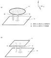
ここで、モノポールアンテナを低背化したものとしてトップローディング型モノポールアンテナがある(例えば、非特許文献1参照)。従来のトップローディング型モノポールアンテナの構造を図20に示す。図20(a)は斜視図、(b)はYZ面に直交して見た平面図である。このトップローディング型モノポールアンテナはトップローディング形状の電極(以下、トップロード電極)11と、トップロード電極11に対向して設けられる地板導体14と地板導体14上の給電点と上記トップロード電極11を電気的に接続する給電素子12からなる。上記トップロード電極11と地板導体14とを電気的に接続する短絡導体13はインピーダンスマッチングを良くするために必要に応じて設けられる。ここで、給電点15に給電用同軸ケーブルの中心導体16が接続され、給電用同軸ケーブルの地板導体17は地板導体14に接続される。ここで、給電素子12と短絡導体13は一般的に900MHzの共振周波数を持つアンテナであれば直径1mm程度の導電体(銅など)の導線が用いられる。
【0004】
この従来例のトップローディング型モノポールアンテナは給電素子12の上部に円形平板形状のトップロード電極11を給電素子12と接続して構成したものである。円形平板形状の電極11を用いることで、周波数900MHzであれば1/4波長で83mmの高さが必要であったモノポールアンテナ装置の高さを30〜40mmに低背化できる。
【0005】
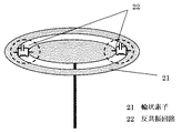
さらに複数の共振周波数を有するアンテナとして、トップローディング型モノポールアンテナを用いた2共振アンテナの構造が提案されている(例えば、特許文献1参照)。このアンテナの構成を図21に示す。これはトップローディング形状の電極11の周囲に輪状素子21を配置し、輪状素子21とトップローディング形状の電極11は、コイルおよびコンデンサで形成される反共振回路22を用いて接続する。共振周波数をそれぞれ第1の周波数、第2の周波数とすると、第1の周波数はトップロード電極11と給電素子12により励振される周波数で、第2の周波数は輪状素子21もトップローディング負荷として加わり輪状素子21とトップロード電極11と給電素子12から励振される周波数である。反共振回路22は第1の周波数に対する反共振回路で、第1の周波数においては輪状素子21が接続していない状態と等価にするための機能を持つ。
【0006】
【発明が解決しようとする課題】
次に、従来例に関わる問題点であり、本発明が解決しようとする課題について説明する。
【0007】
第1の課題は、低背時にインピーダンスの整合が困難になるという問題である。
【0008】
アンテナの低背化により、トップロード電極11と地板導体14との間隔が小さくなる。
【0009】
一般に地板導体14を用いたアンテナでは地板導体14が存在することで、地板導体14を挟んで対称に、トップロード電極11上を流れる、地板導体14と平行な電流に対しては、地板導体14から等距離離れて逆向きの電流が存在することと等価になる。これをイメージ電流という。
【0010】
間隔が小さいと、トップロード電極による放射電界はイメージ電流による放射電界に打ち消され小さくなる。これは給電点15の電圧が低くなることを意味している。アンテナに流れる電流は低背化する前と比べ大きく変化しないため、電圧の低下に伴い、入力インピーダンスが低下するのである。
【0011】
第2の課題は、低背時に帯域が狭くなるという課題である。アンテナを使用する通信システムにより使用される帯域は決まっており、そのため、低くする高さにも制限がある。
【0012】
第3の課題は、複数の異なる周波数で共振させることである。近年、移動体通信においては多くの周波数が用いられている。従来の技術に関しての項で例としてあげた900MHzは一般にPDC800MHz帯といわれる周波数(810〜960MHz)を想定している。携帯電話においては上記の800MHz帯以外に1.5GHz帯も使用しており、本発明の使用用途として車載の携帯電話用アンテナを想定しているので、両方の周波数をカバーする必要がある。しかしながら、トップローディングモノポールアンテナを用いた多周波への対応は一般的には行われておらず、従来例で示した構成においても、より簡便に量産するためには反共振回路を使用しない構成が望まれる。
【0013】
第4の課題は小形化する課題である。車内設置するアンテナとしては特に小形形状が望ましい。通常のトップロード型モノポールアンテナは上述のようにアンテナを低背化するとトップロード電極11が大きくなり、地板導体14の必要な大きさも増大する。車内では十分な地板の大きさがとれないことが多いので、アンテナを低背にする高さも制限がある。従来のトップロード型モノポールアンテナでは地板導体14の大きさの制約から共振周波数が900MHzのトップローディングモノポールアンテナにおいてはアンテナ高が30〜40mmと高くなり不向きであった。
【0014】
【課題を解決するための手段】
本発明のアンテナ装置は上記課題を解決するために、地板導体と、上記地板導体と対向して設けられトップローディング部を構成する電極と、給電点と上記電極とを接続する給電素子と、上記電極と上記地板導体とを接続するための短絡導体を備えたトップローディング型モノポールアンテナ装置であって、上記線状素子は断面の外周長が0.03波長以上である構成とする。
【0015】
また、地板導体と、上記地板導体と対向して設けられトップローディング部を構成する電極と、給電点と上記電極とを接続する給電素子と、上記電極と上記接続導体とを接続するための短絡導体を備えたトップローディング型モノポールアンテナ装置であって、上記短絡導体は断面の外周長が0.03波長以上であること構成とする。
【0016】
さらに、地板導体と、上記地板導体と対向して設けられトップローディング部を構成する電極と、給電点と上記電極とを接続する給電素子と、上記電極と上記接続導体とを接続するための短絡導体を備えたトップローディング型モノポールアンテナ装置であって、上記給電素子および上記短絡導体は断面の外周長が0.03波長以上である構成とする。
【0017】
ここで、上記トップローディング部を構成する電極は折り曲げ部を有しても良い。
【0018】
さらに、上記トップローディング部を有する電極は方形であっても良い。
【0019】
また、上記給電点に対して、上記地板導体上に設けた整合回路を介して接続してもよい。
【0020】
また、上記地板導体は円形平板形状であっても良い。
【0021】
また、上記給電導体の両端の間に位置する中間位置と、上記地板導体とを接続するための短絡制御導体をさらに備えても良い。
【0022】
また、本発明のアンテナ装置は、地板導体と、上記地板導体と対向して設けられトップローディング部を構成する電極と、給電点と上記電極とを接続する給電素子と、一端が上記地板導体に接続する第1の導体板を備えたトップローディング型モノポールアンテナ装置であって、第1の導体板は、上記線状素子および上記短絡導体に対し平行な部分を有する構成とする。
【0023】
ここで、第1の導体板は前記第1の導体板の共振周波数の波長に対し巾0.01波長以上であっても良い。
【0024】
また、第1の導体板と前記給電導体の間隔は記第1の導体板の共振周波数の波長に対し0.01波長以内であってもよい。
【0025】
さらに第1の導体板は前記アンテナ装置の動作中心周波数における1/4波長の長さであっても良い。
【0026】
また、一端が上記地板導体に接続する第1の導体板であって、第1の導体板は、上記線状素子および上記短絡導体に対し平行であって、上記電極に対して平行に併設することを特徴する第1の導体板を備えても良い。
【0027】
ここで、第1の導体板は前記第1の導体板の共振周波数の波長に対し巾0.01波長以上であっても良い。
【0028】
さらに、第1の導体板と前記給電導体の間隔は前記第1の導体板の共振周波数の波長に対し0.01波長以内であってもよい。
【0029】
また、第1の導体板は前記アンテナ装置の動作中心周波数における1/4波長の長さであっても良い。
【0030】
さらに、本発明のアンテナ装置は、地板導体と、上記地板導体と対向して設けられトップローディング部を構成する電極と、給電点と上記電極とを接続する給電素子と、上記地板導体および上記電極と平行な第2の導体板を備えた構成とする。
【0031】
ここで、第2の導体板は前記アンテナ装置の動作中心周波数における1/2波長の長さであっても良い。
【0032】
さらに、第2の導体板は上記地板導体および上記電極と平行でも良い。
【0033】
また、第2の導体板は前記アンテナ装置の動作中心周波数における1/2波長の長さであっても良い。
【0034】
また、本発明の通信システムは、車両内部に設置された受信機と、車両ルーフまたはトランクルーフ上に設置され、かつ上記の受信機に接続された本発明のモノポールアンテナ装置を用いた構成とする。
【0035】
さらに、車両内部に設置された受信機と、上記車両内部に設置され、かつ上記の受信機に接続された本発明のモノポールアンテナ装置を用いた構成とする。
【0036】
ここで、上記モノポールアンテナ装置を、上記車両のフロントウインドまたはリアウインド近傍に設置するときにそれぞれ、上記モノポールアンテナの短絡導体と上記給電素子を結ぶ方向と直交する方向に、上記フロントウインドまたは上記リアウインドが位置するように上記モノポールアンテナ装置を設置しても良い。
【0037】
また、上記車両内に凹部を形成し、上記凹部内に上記モノポールアンテナ装置を設置し、上記凹部の開口部をレドームにより覆っても良い。
【0038】
【発明の実施の形態】
以下、図面を参照して本発明に関わる実施の形態について説明する。なお、図面においては、同様の部分については同一の符号を付している。
【0039】
(実施の形態1)
まず、図1から図5を用いて、本発明のアンテナ装置の動作原理を説明する。
【0040】
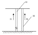
図1に本発明のトップローディング型モノポールアンテナ装置の構成を示す。従来の技術と比べて異なるのは、直径0.01波長以上の給電素子31および直径0.01波長以上の短絡導体32を用いることで給電点でのインピーダンスマッチングを可能とした点である。この給電素子、短絡導体の直径は従来の技術で900MHzの共振周波数であれば1mmの直径の導体を用いていたことと比較すると、外観の面では直径3mm以上の太い導線を用いている点で異なる。また、直径0.01波長以上の給電素子31および直径0.01波長以上の短絡導体32を用いるということは、すなわち断面の周囲長がそれぞれ0.03波長以上となることを意味する。
【0041】
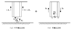
ここで、インピーダンスマッチングの原理を説明する。図2に示すのはトップローディング型モノポールアンテナに流れる電流の概念図である。本発明のアンテナの電流は放射に関係する不平衡伝送系と、放射には関係せずアンテナのインピーダンスのみに関係する平衡伝送系に分けて解析できる。
【0042】
図3に不平衡伝送系と平衡伝送系を分けて示し説明する。
【0043】
さらに、図3(a)のaa’からアンテナをみたインピーダンスをZuとし、図3(b)のbb’からアンテナを見たインピーダンスをZbとすると、
【0044】
【数1】
【0045】
【数2】
【0046】
の関係がある。
【0047】
さらに、次の連立方程式が図3において成立する。
【0048】
【数3】
【0049】
【数4】
【0050】
【数5】
【0051】
【数6】
【0052】
よって、本発明のアンテナの給電点15におけるインピーダンスZは
【0053】
【数7】
【0054】
で表せる。
【0055】
これは、本発明のアンテナの入力インピーダンスZはνiの関数であることを示している。
【0056】
電流分配率νiは給電素子31の半径ρ1、短絡導体32の半径ρ2、給電素子31と短絡導体32の中心距離sが決まれば、次式で求まる。
【0057】
【数8】
【0058】
これから、ρ1、ρ2の経を制御することで入力インピーダンスZが制御できることがわかる。(8)式は短絡導体32の半径ρ2を増加すれば入力インピーダンスZが増加し、給電素子31の半径ρ1を増加すれば入力インピーダンスZが減少することを意味する。
【0059】
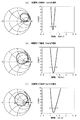
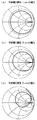
図4に給電素子31の直径を変化したとき、図5に短絡導体32の直径を変化したときの本発明のアンテナの入力インピーダンスの変化を示しこれを確かめる。
【0060】
図4(a)の左の図に示すのはスミスチャートと呼ぶインピーダンスの変化を示すための図である。スミスチャートの中心を通る線A−A’をスミスチャートの円弧が横切る位置Bが入力インピーダンスを表している。線A−A’においてインピーダンスはA側が低くA’側が高い。中心位置が整合している点である。ここで図4(b)、(c)と給電素子31の直径を大きくすると入力インピーダンスは低くなっている。また、図4(b)である給電素子31の直径3mmでほぼ整合しており、給電素子31の直径を変化させることで入力インピーダンスを整合できることがわかる。また、図5において短絡導体32の直径を変化させたときのインピーダンス変化からわかるように、短絡導体32の直径を大きくすることで、入力インピーダンスは高くなる。短絡導体32の直径だけを変化させても入力インピーダンスは整合できる。この結果は(8)式の結果と良く合っており、入力インピーダンスの課題に対しては給電素子31または短絡導体32の直径を変化させることで解決できたことがわかる。
【0061】
帯域幅に関しては、給電素子31の直径と短絡導体32の直径を適切に選択することで広げることが出来る。図4(a)、(b)、(c)は上述のように給電素子31の直径を変化させた時のインピーダンスの変化で、右側の図から帯域幅の拡大がわかる。これを以下に説明する。図4(a)の右側に示した図は給電素子31の直径を変化したときのVSWRの変化を示す図である。この図の横軸は周波数、縦軸はVSWRである。図中にC−C’で示す横線がVSWR=3の線で、VSWR=3以下をこのアンテナの使用可能な帯域と定義する。給電素子31の直径が1mmの図4(a)においてはVSWR=3を下回る帯域幅は80MHzで、給電素子31の直径が3mmの図4(b)では150MHz、給電素子31の直径が3mmの図4(b)では190MHzとなり、給電素子31の直径が大きくなるほど帯域が増加することがわかる。ただし、上述したように給電素子31の直径を大きくすると入力インピーダンスが低下するので、短絡導体32を適切な太さにして入力インピーダンスを整合させる必要がある。すなわち給電素子31と短絡導体32の直径を900MHzであればともに3mm以上つまり0.01波長以上の直径とすることで広帯域化が出来ることがわかる。
【0062】
図8は、本発明の第1の実施例に関わるトップローディング型モノポールアンテナ装置の構成を示す斜視図である。この第1の実施の形態のトップローディング型モノポールアンテナ装置は1点目のインピーダンスの整合に関する課題および2点目の帯域に関する課題に対する解決手段を提供するものである。
【0063】
図8に図示される第1の実施例に関わるアンテナは以下の点で従来のアンテナ形状と異なることを特徴としている。
【0064】
(1)線状素子の断面の周囲長が0.03波長となる。具体的には共振周波数900MHzのアンテナに対しては直径が約3mm以上の導体あるいは中空導体で線状素子が構成される。
【0065】
(2)短絡導体の断面の周囲長が0.03波長となる。具体的には共振周波数900MHzのアンテナに対しては直径が約3mm以上の導体あるいは中空導体で線状素子が構成される。
【0066】
図8に示すように本発明のトップローディング型モノポールアンテナ装置は、トップローディングのための円形平板形状の電極と電極と対向して設けられ平板形状の地板導体と給電点と電極とを電気的に接続する断面の周囲長が0.03波長以上の給電素子31と、電極と地板導体とを電気的に接続する断面の周囲長が0.03波長以上の短絡導体32から構成される。ここで、給電点には給電用同軸ケーブルの中心導体が接続され、給電用同軸ケーブルの地板導体は本発明のアンテナ装置の地板導体に接続される。
【0067】
本実施の形態において、電極の半径は1/4波長ないし1/6波長となる。また、地板導体の半径は好ましくは1/2波長以上に設定される。さらに当該アンテナの高さは、実施の形態においては1/8波長ないし1/10波長である。なお、本実施の形態およびそれ以降で説明する実施の形態および変形例において、1波長は当該アンテナが動作する動作中心周波数に対応する長さである。
【0068】
(実施の形態2)
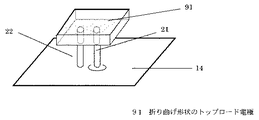
図9は本発明の第2の実施の形態に関わるトップローディング型モノポールアンテナの構成を示す斜視図である。図9に示す実施例は折り曲げられたトップロード電極91、給電素子31、短絡導体32、地板導体14から構成される。本実施例に関わるトップローディング型モノポールアンテナ装置は、第1の実施の形態のアンテナ装置と比較し、トップローディング電極部が折り曲げ部を有する点で異なる。
【0069】
図9のようにトップローディング部が折り曲げられることで、電極の上部から見たときの投影面積を小さくできる。さらに、トップローディング電極91の表面積においても折り曲げ部を有することで、折り曲げられた先端部と地板電極間に生じる容量性のリアクタンス成分が大きくなり、表面積が小さくなり、小型化に寄与する。
【0070】
(実施の形態3)
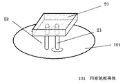
図10は本発明の第3の実施の形態にかかわるトップローディング型モノポールアンテナの構成を示す斜視図である。図10に示す実施例はトップロード電極91、給電素子31、短絡導体32、円形地板導体101から構成される。本実施例にかかわるトップローディング型モノポールアンテナ装置は第1の実施の形態のアンテナと比較し、地板導体が円形形状をしている点で異なる。このように円形の形状とすることで本実施例のトップローディング型モノポールアンテナを設置する際に設置方向を自由に回転することが可能となる。
【0071】
(実施の形態4)
図11は本発明の第4の実施の形態にかかわるトップローディング型モノポールアンテナの構成を示す斜視図である。図11に示す実施例はトップロード電極91、給電素子31、短絡導体32、地板導体14、給電素子13の一部と地板導体14を接続するインピーダンス調整用タップ111から構成される。本実施例にかかわるトップローディング型モノポールアンテナは、地板と給電素子を接続するインピーダンス調整用タップ111を有する点で第1の実施の形態と異なる。この導線によって給電点での電流量を調整することが出来る。入力インピーダンスは給電点での電圧と電流により決まるので、インピーダンス調整用タップ111を用いることで入力インピーダンスを微調整することが可能となる。
【0072】
(実施の形態5)
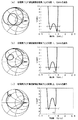
図6および図7および図12から図15は本発明によるモノポールアンテナの第5の実施の形態に関係する図を示すものである。図6および図7を用いて、無給電素子をもちいて複数の周波数で共振させる動作原理について説明する。図6のように片側を短絡した無給電素子を併設すると、前記無給電素子の長さが約1/4波長に相当する任意の周波数で前記無給電素子を共振させることが出来る。図7は給電素子31と片側短絡無給電素子81との間隔を変えたときの、入力インピーダンスの変化を示す図である。右側の図がVSWRと周波数の関係を示す図で、C−C’に示すVSWR=3の線を高い周波数で下回る部分F2が片側短絡無給電素子により生じた共振である。図7(a)は給電素子31と片側短絡無給電素子の間隔が1.0mmのときのVSWR変化を示しているが、一方図7(b)の給電素子31と片側短絡無給電素子の間隔が1.5mmのときのVSWR変化では共振周波数F2の時のVSWRの値は高くなり、図7(c)ではさらに高くなっている。このことから、無給電素子は給電素子との間隔が小さいほど放射電力が大きくなることがわかる。つまり、1.5GHzで2mm以下つまり0.1波長以下に給電素子31と片側短絡無給電素子の間隔を近づけることによって、2周波で共振するアンテナを実現し課題を解決できることがわかった。
【0073】
図12に示す実施例はトップロード電極11、給電素子31、短絡導体32、地板導体14、折り曲げ形状の片側短絡1/4波長無給電素子121から構成される。
【0074】
第1の実施の形態との違いは、折り曲げ形状の片側短絡1/4波長無給電素子121を有することである。この折り曲げ形状の片側短絡1/4波長無給電素子121は課題を解決する手段の項で前述したように給電素子31およびトップロード電極11からの誘導電流によりアンテナとして機能する。折り曲げ形状の片側短絡1/4波長無給電素子121の共振の中心周波数は任意に設定することが出来る。この時の折り曲げ形状の片側短絡1/4波長無給電素子121の長さは所望の共振の中心周波数の波長に対して1/4波長となることが望ましい。
【0075】
折り曲げ形状の片側短絡1/4波長無給電素子121の巾を変化させたときのインピーダンス変化を図13に示す。図13(a)が巾3mm、(b)が巾5mm、(c)が巾7mmの場合である。VSWRと周波数の関係を見ると、VSWR=3の位置を無給電素子による共振周波数F2で下回る部分は(a)の巾3mmでは下がりきらず(b)の巾5mm以降で生じることがわかる。(a)の場合を境界線と考えて、折り曲げ形状の片側短絡1/4波長無給電素子121は1.5GHz帯において巾3mm以上つまり0.15波長以上であればよいことがわかった。
【0076】
折り曲げ形状の片側短絡1/4波長無給電素子121は図12に示すように複数回折り曲げられた形状でも良いし、図6の61にしめすように1度だけ折り曲げられた形状でも良い。
【0077】
図14に示すのは、本実施例の異なる構成である。ここでは、折り曲げ形状の片側短絡1/4波長無給電素子121ではなく、両側開放の1/2波長無給電素子141である。この両側開放の1/2波長無給電素子141においても、トップロード電極11からの誘導電流によりアンテナとして機能する。この両側開放の1/2波長無給電素子141の長さは1/2波長となるのが望ましい。なぜなら、両方の端部が開放されているため両端での電流がゼロとなり、両側開放の1/2波長無給電素子141の中央の電流が最大となる。これは1/2波長の時に共振となる条件だからである。
【0078】
さらに図15に折り曲げ形状の片側短絡1/4波長無給電素子121を用い、折り曲げたトップロード電極とした構成として示した。図15の形状とすることで、小型で2つの周波数に共振を有するモノポールアンテナを実現できる。
【0079】
ここでは、給電素子31、短絡導体32として、断面の外周長が0.03波長以上の場合について説明したが、断面の外周長が0.03波長以下の場合においても同様の効果が得られる。
【0080】
さらに、短絡導体32がない場合においても折り曲げ形状の片側短絡1/4波長無給電素子121または両側開放の1/2波長無給電素子141を設けることで2周波化が図れる。
【0081】
さらに、折り曲げ形状の片側短絡1/4波長無給電素子121または両側開放の1/2波長無給電素子141を複数設置することで、2周波数以上、たとえば3周波数、4周波数に適合するダイポールアンテナ装置を提供することができる。
【0082】
(実施の形態6)
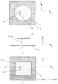
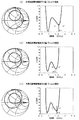
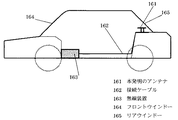
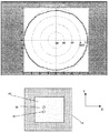
車内設置に関しては、小型のアンテナ形状とすることで解決する。本発明のアンテナは900MHzの共振周波数で、高さ20mm、巾30mm、奥行き30mmの大きさで実現できる。従来技術においては同じ共振周波数において高さ40mm、巾、奥行きは60mm程度の大きさであった。小型化することでアンテナ下方に必要となる地板導体の寸法を小さくすることができ、それにより地板導体の面積の小さい車内においても設置することが出来る。図16、17は本発明によるモノポールアンテナの第6の実施の形態に関係する図を示すものである。図16に示すのは車内における本発明のアンテナ161の設置方法である。本発明のアンテナは車内のリアウインドー165側に設置する。この時、無線装置163は車内に置き、無線装置163と本発明のアンテナ161は接続ケーブル162で接続する。本発明のアンテナ161は短絡導体32を有している。図17に本発明のアンテナの水平面の指向性を示す。この図17に示すように、短絡導体32と給電素子31を結んだ線と直交する方向に感度が高くなるので、この方向がリアウインドー165側になるように位置させることで車両の前後方向の感度が高くなる。
【0083】
本発明のアンテナは従来のトップロード型モノポールアンテナに比べトップロード電極11が小さくなるため地板導体14の必要となる大きさも小さくできる。それにより、車内設置に適している。車内に置くことで接続ケーブル162も短くでき、接続ケーブル162による車両ノイズ混入の確率を抑えさらに信号の劣化も抑えることが出来る。
【0084】
さらに、本発明のアンテナ161はフロントウインドー164側に位置しても良い。
【0085】
(実施の形態7)
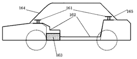
図17は本発明によるモノポールアンテナの第7の実施の形態に関係する図を示すものである。図17に示すのは本発明のアンテナ161を車内に2つ配置するときの設置方法である。本発明の実施例6と異なり、2つのアンテナを設置する時には、1つはフロントウインドー164寄りに設置し、他方はリアウインドー165寄りに設置する。車両両サイド方向へも本発明のアンテナ161が2つあることで高い指向性が得られるので、車両に対し全方向に高い指向性を得ることが出来る。
【0086】
ここで、フロントウインドー164方向およびリアウインドー165方向に各2つずつのアンテナを設置した場合は、同じウインドー側にあるアンテナ間の距離の差によって、ダイバーシチー効果が得られ、より安定した感度が期待できる。
【0087】
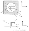
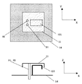
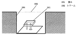
(実施の形態8)
図18は本発明によるモノポールアンテナの第8の実施の形態に関係する図を示すものである。図19に示すのは本発明のアンテナ161を車内あるいは車外に設置するときに目立たなく設置するための設置方法である。本発明のアンテナ161を窪み191内に設置し、レドーム192を被せる。レドーム192は導電体以外の材料で作成する。
【0088】
【発明の効果】
これまで、述べたように本発明によれば、低背形状で整合が可能なモノポールアンテナを提供できる。
【0089】
さらに本発明によれば、トップロード部の電極が小さなモノポールアンテナを提供できる。
【0090】
さらに本発明によれば、広帯域な低背形状のモノポールアンテナを提供できる。
【0091】
さらに本発明によれば、車内設置が可能なモノポールアンテナを提供できる。
【0092】
さらに本発明によれば、目立たず設置可能なモノポールアンテナを提供できる。
【0093】
以上のことから、 本発明によって低背形状で車内置きに適したモノポールアンテナを提供でき、車両の方向によらず高い感度を得ることが出来る。
【図面の簡単な説明】
【図1】本発明のアンテナの構成を示す図
【図2】本発明のアンテナの電流の概念図
【図3】本発明のアンテナの電流を平衡系と不平衡系に分けた概念図
【図4】給電素子の直径を変化したときのインピーダンスの変化を示す図
【図5】短絡導体の直径を変化したときのインピーダンス変化を示す図
【図6】本発明の2共振アンテナの構成図
【図7】給電素子と片側短絡無給電素子の間隔を変えたときの入力インピーダンスの変化を示す図
【図8】本発明の第1の実施の形態のモノポールアンテナの斜視図
【図9】本発明の第2の実施の形態のモノポールアンテナの斜視図
【図10】本発明の第3の実施の形態のモノポールアンテナの斜視図
【図11】本発明の第4の実施の形態のモノポールアンテナの斜視図
【図12】本発明の第5の実施の形態のモノポールアンテナの斜視図
【図13】片側短絡無給電素子の巾を変えたときの入力インピーダンスの変化を示す図
【図14】本発明の第5の実施の形態のモノポールアンテナの斜視図
【図15】本発明の第5の実施の形態のモノポールアンテナの斜視図
【図16】本発明の第6の実施の形態の通信システムの構成を示す図
【図17】本発明の第7の実施の形態のアンテナの水平面指向性を示す図
【図18】本発明の第8の実施の形態の通信システムの構成を示す図
【図19】本発明の第8の実施の形態の通信システムの構成を示す図
【図20】従来のトップロード型モノポールアンテナを示す図
【図21】従来の2共振トップロード型モノポールアンテナを示す図
【符号の説明】
11 トップロード電極
12 給電素子
13 短絡導体
14 地板導体
15 給電点
16 同軸ケーブル中心導体
17 同軸ケーブル地板導体
21 輪状素子
22 反共振回路
31 直径0.01波長以上の給電素子
32 直径0.01波長以上の短絡導体
61 片側短絡1/4波長無給電素子
81 方形のトップロード電極
91 折り曲げ形状のトップロード電極
101 円形地板導体
111 インピーダンス調整用タップ
121 折り曲げ形状の片側短絡1/4波長無給電素子
141 両側開放の1/2波長無給電素子
161 本発明のアンテナ
162 接続ケーブル
163 無線装置
164 フロントウインドー
165 リアウインドー
191 窪み
192 レドーム[0001]
TECHNICAL FIELD OF THE INVENTION
The present invention relates to a monopole antenna device and an antenna system used for a mobile radio device. In particular, the present invention relates to a monopole antenna device and an antenna system to be mounted in a vehicle for use in a vehicle.
[0002]
[Prior art]
A monopole antenna device is a general antenna as a vehicle-mounted antenna. The monopole antenna device is a linear antenna and often has a height of 1/4 wavelength or 3/4 wavelength. In the case of a frequency of 900 MHz used for a mobile phone, a quarter wavelength is 83 mm and a quarter wavelength is 249 mm, and the size becomes an issue as an antenna device placed on the roof of a vehicle or in a vehicle.
[0003]
Here, as a monopole antenna having a reduced height, there is a top-loading type monopole antenna (for example, see Non-Patent Document 1). FIG. 20 shows the structure of a conventional top-loading type monopole antenna. FIG. 20A is a perspective view, and FIG. 20B is a plan view seen perpendicular to the YZ plane. This top-loading type monopole antenna includes a top-loading-shaped electrode (hereinafter referred to as a top-load electrode) 11, a ground conductor 14 provided to face the top-load electrode 11, a feed point on the ground-plate conductor 14, and the top-load electrode 11 Are electrically connected to each other. The short-circuit conductor 13 for electrically connecting the top load electrode 11 and the ground plane conductor 14 is provided as necessary to improve impedance matching. Here, the center conductor 16 of the power supply coaxial cable is connected to the power supply point 15, and the ground plane conductor 17 of the power supply coaxial cable is connected to the ground plane conductor 14. Here, as the feed element 12 and the short-circuit conductor 13, a conductor of a conductor (such as copper) having a diameter of about 1 mm is generally used as long as the antenna has a resonance frequency of 900 MHz.
[0004]
This conventional top-loading type monopole antenna has a configuration in which a top load electrode 11 in the form of a circular flat plate is connected to the feed element 12 above the feed element 12. By using the circular plate-shaped electrode 11, the height of the monopole antenna device, which required a height of 83 mm at a quarter wavelength at a frequency of 900 MHz, can be reduced to 30 to 40 mm.
[0005]
Further, as an antenna having a plurality of resonance frequencies, a two-resonance antenna structure using a top-loading monopole antenna has been proposed (for example, see Patent Document 1). FIG. 21 shows the configuration of this antenna. In this method, the ring-shaped element 21 is arranged around the top-loading-shaped electrode 11, and the ring-shaped element 21 and the top-loading-shaped electrode 11 are connected by using an anti-resonance circuit 22 formed by a coil and a capacitor. Assuming that the resonance frequencies are a first frequency and a second frequency, respectively, the first frequency is a frequency excited by the top load electrode 11 and the feed element 12, and the second frequency is that the ring element 21 is also applied as a top loading load. This is the frequency excited from the ring element 21, the top load electrode 11, and the power supply element 12. The anti-resonance circuit 22 is an anti-resonance circuit for the first frequency, and has a function of making the state at the first frequency equivalent to a state where the ring-shaped element 21 is not connected.
[0006]
[Problems to be solved by the invention]
Next, problems which are related to the conventional example and which are to be solved by the present invention will be described.
[0007]
The first problem is that impedance matching becomes difficult when the height is low.
[0008]
As the height of the antenna is reduced, the distance between the top load electrode 11 and the ground plane conductor 14 is reduced.
[0009]
In general, in the antenna using the ground plane conductor 14, the presence of the ground plane conductor 14 causes the ground plane conductor 14 to flow symmetrically across the ground plane conductor 14 on the top load electrode 11 and parallel to the ground plane conductor 14. This is equivalent to the presence of a current in the opposite direction at an equal distance from. This is called an image current.
[0010]
If the interval is small, the radiated electric field due to the top load electrode is canceled out by the radiated electric field due to the image current, and becomes smaller. This means that the voltage at the feeding point 15 decreases. Since the current flowing through the antenna does not change much as compared to before the height is reduced, the input impedance decreases as the voltage decreases.
[0011]
The second problem is that the band becomes narrow when the height is low. The band used by a communication system using an antenna is fixed, and therefore the height to be lowered is also limited.
[0012]
A third problem is to resonate at a plurality of different frequencies. In recent years, many frequencies have been used in mobile communication. The 900 MHz mentioned as an example in the section related to the prior art is assumed to be a frequency (810 to 960 MHz) generally called a PDC 800 MHz band. In a mobile phone, a 1.5 GHz band is also used in addition to the 800 MHz band, and an antenna for a mobile phone mounted on a vehicle is assumed to be used in the present invention. Therefore, both frequencies need to be covered. However, multi-frequency response using a top-loading monopole antenna is not generally performed, and even in the configuration shown in the conventional example, a configuration that does not use an anti-resonance circuit for easier mass production. Is desired.
[0013]
The fourth problem is to reduce the size. It is particularly desirable for the antenna to be installed in the vehicle to have a small size. As described above, when the height of the normal top-load type monopole antenna is reduced, the top-load electrode 11 becomes large, and the required size of the ground conductor 14 also increases. In many cases, the height of the antenna is limited because the size of the ground plane cannot be sufficiently large in the vehicle. The conventional top-load type monopole antenna is not suitable because the height of the top-loading monopole antenna having a resonance frequency of 900 MHz is as high as 30 to 40 mm due to the restriction of the size of the ground conductor 14.
[0014]
[Means for Solving the Problems]
In order to solve the above problem, the antenna device of the present invention includes a ground plane conductor, an electrode that is provided to face the ground plane conductor and forms a top loading portion, a feed element that connects a feed point and the electrode, A top-loading type monopole antenna device having a short-circuit conductor for connecting an electrode to the ground conductor, wherein the linear element has an outer peripheral length of 0.03 wavelength or more in cross section.
[0015]
Also, a ground plane conductor, an electrode provided opposite to the ground plane conductor and constituting a top loading portion, a power supply element for connecting a power supply point to the electrode, and a short circuit for connecting the electrode and the connection conductor. A top-loading monopole antenna device having a conductor, wherein the short-circuit conductor has a cross-sectional outer peripheral length of 0.03 wavelength or more.
[0016]
Furthermore, a ground plane conductor, an electrode provided opposite to the ground plane conductor and constituting a top loading portion, a feed element for connecting a feed point and the electrode, and a short circuit for connecting the electrode and the connection conductor. A top-loading monopole antenna device having a conductor, wherein the feed element and the short-circuit conductor have a cross-sectional outer peripheral length of 0.03 wavelength or more.
[0017]
Here, the electrode constituting the top loading portion may have a bent portion.
[0018]
Further, the electrode having the top loading portion may be rectangular.
[0019]
Further, the power supply point may be connected via a matching circuit provided on the ground plane conductor.
[0020]
Further, the ground plate conductor may have a circular flat plate shape.
[0021]
In addition, a short-circuit control conductor for connecting an intermediate position located between both ends of the power supply conductor and the ground plane conductor may be further provided.
[0022]
In addition, the antenna device of the present invention includes a ground plane conductor, an electrode that is provided to face the ground plane conductor and forms a top loading portion, a feed element that connects a feed point and the electrode, and one end is connected to the ground plane conductor. A top-loading type monopole antenna device including a first conductor plate to be connected, wherein the first conductor plate has a portion parallel to the linear element and the short-circuit conductor.
[0023]
Here, the first conductor plate may have a width of 0.01 wavelength or more with respect to the wavelength of the resonance frequency of the first conductor plate.
[0024]
The distance between the first conductor plate and the power supply conductor may be within 0.01 wavelength with respect to the wavelength of the resonance frequency of the first conductor plate.
[0025]
Further, the first conductor plate may have a length of 波長 wavelength at an operation center frequency of the antenna device.
[0026]
Further, one end is a first conductor plate connected to the ground plane conductor, and the first conductor plate is provided in parallel with the linear element and the short-circuit conductor and in parallel with the electrode. A first conductor plate characterized by the above feature may be provided.
[0027]
Here, the first conductor plate may have a width of 0.01 wavelength or more with respect to the wavelength of the resonance frequency of the first conductor plate.
[0028]
Furthermore, the distance between the first conductor plate and the power supply conductor may be within 0.01 wavelength with respect to the wavelength of the resonance frequency of the first conductor plate.
[0029]
Further, the first conductor plate may have a length of 1 / wavelength at an operation center frequency of the antenna device.
[0030]
Further, the antenna device of the present invention includes a ground plane conductor, an electrode that is provided to face the ground plane conductor and forms a top loading portion, a feed element that connects a feed point and the electrode, the ground plane conductor and the electrode. And a second conductor plate parallel to the second conductor plate.
[0031]
Here, the second conductor plate may have a length of 波長 wavelength at an operation center frequency of the antenna device.
[0032]
Further, the second conductor plate may be parallel to the ground plate conductor and the electrode.
[0033]
Further, the second conductor plate may have a length of 波長 wavelength at an operation center frequency of the antenna device.
[0034]
Further, the communication system of the present invention has a receiver installed inside the vehicle, a configuration using the monopole antenna device of the present invention installed on the vehicle roof or trunk roof, and connected to the receiver. I do.
[0035]
Further, a configuration is provided using a receiver installed inside the vehicle and a monopole antenna device of the present invention installed inside the vehicle and connected to the receiver.
[0036]
Here, when the monopole antenna device is installed in the vicinity of the front window or the rear window of the vehicle, the front window or the direction perpendicular to the direction connecting the short-circuit conductor of the monopole antenna and the feed element is respectively set. The monopole antenna device may be installed so that the rear window is located.
[0037]
Further, a recess may be formed in the vehicle, the monopole antenna device may be installed in the recess, and the opening of the recess may be covered by a radome.
[0038]
BEST MODE FOR CARRYING OUT THE INVENTION
Hereinafter, embodiments of the present invention will be described with reference to the drawings. In the drawings, the same parts are denoted by the same reference numerals.
[0039]
(Embodiment 1)
First, the operation principle of the antenna device of the present invention will be described with reference to FIGS.
[0040]
FIG. 1 shows a configuration of a top-loading monopole antenna device of the present invention. The difference from the prior art is that impedance matching at the feeding point is enabled by using the feeding element 31 having a diameter of 0.01 wavelength or more and the short-circuit conductor 32 having a diameter of 0.01 wavelength or more. The diameter of the feeding element and the short-circuiting conductor is 1 mm in diameter if the resonance frequency is 900 MHz in the conventional technology. different. The use of the feeding element 31 having a diameter of 0.01 wavelength or more and the short-circuit conductor 32 having a diameter of 0.01 wavelength or more means that the circumference of the cross section is 0.03 wavelength or more.
[0041]
Here, the principle of impedance matching will be described. FIG. 2 is a conceptual diagram of a current flowing through a top-loading type monopole antenna. The current of the antenna of the present invention can be analyzed separately into an unbalanced transmission system related to radiation and a balanced transmission system related only to the antenna impedance without being related to radiation.
[0042]
FIG. 3 illustrates the unbalanced transmission system and the balanced transmission system separately.
[0043]
Further, assuming that the impedance when the antenna is viewed from aa ′ in FIG. 3A is Zu and the impedance when the antenna is viewed from bb ′ in FIG. 3B is Zb,
[0044]
(Equation 1)
[0045]
(Equation 2)
[0046]
There is a relationship.
[0047]
Further, the following simultaneous equations are established in FIG.
[0048]
[Equation 3]
[0049]
(Equation 4)
[0050]
(Equation 5)
[0051]
(Equation 6)
[0052]
Therefore, the impedance Z at the feeding point 15 of the antenna of the present invention is
[0053]
(Equation 7)
[0054]
Can be represented by
[0055]
This indicates that the input impedance Z of the antenna of the present invention is a function of νi.
[0056]
The current distribution ratio νi can be obtained by the following equation if the radius ρ1 of the feed element 31 and the radius ρ2 of the short-circuit conductor 32 and the center distance s between the feed element 31 and the short-circuit conductor 32 are determined.
[0057]
(Equation 8)
[0058]
From this, it is understood that the input impedance Z can be controlled by controlling the paths of ρ1 and ρ2. Equation (8) means that if the radius ρ2 of the short-circuit conductor 32 increases, the input impedance Z increases, and if the radius ρ1 of the feed element 31 increases, the input impedance Z decreases.
[0059]
FIG. 4 shows the change in the input impedance of the antenna of the present invention when the diameter of the feed element 31 is changed, and FIG. 5 shows the change in the input impedance when the diameter of the short-circuit conductor 32 is changed.
[0060]
The diagram on the left side of FIG. 4A is a diagram for illustrating a change in impedance called a Smith chart. The position B where the arc of the Smith chart crosses the line AA 'passing through the center of the Smith chart represents the input impedance. In the line AA ′, the impedance is lower on the A side and higher on the A ′ side. This is the point where the center positions match. Here, when the diameter of the feed element 31 is increased as shown in FIGS. 4B and 4C, the input impedance decreases. In addition, the matching is almost achieved at the diameter of the feeding element 31 of 3 mm shown in FIG. 4B, and it can be seen that the input impedance can be matched by changing the diameter of the feeding element 31. In addition, as can be seen from the change in impedance when the diameter of the short-circuit conductor 32 is changed in FIG. 5, the input impedance increases as the diameter of the short-circuit conductor 32 increases. Even if only the diameter of the short-circuit conductor 32 is changed, the input impedance can be matched. This result agrees well with the result of Expression (8), and it can be seen that the problem of the input impedance could be solved by changing the diameter of the feed element 31 or the short-circuit conductor 32.
[0061]
The bandwidth can be widened by appropriately selecting the diameter of the feed element 31 and the diameter of the short-circuit conductor 32. FIGS. 4A, 4B, and 4C show changes in impedance when the diameter of the feed element 31 is changed as described above. It can be seen from FIG. This will be described below. The diagram shown on the right side of FIG. 4A is a diagram showing a change in VSWR when the diameter of the feed element 31 is changed. In this figure, the horizontal axis is frequency, and the vertical axis is VSWR. In the figure, a horizontal line indicated by CC ′ is a line of VSWR = 3, and VSWR = 3 or less is defined as a usable band of this antenna. In FIG. 4A in which the diameter of the feed element 31 is 1 mm, the bandwidth below VSWR = 3 is 80 MHz. In FIG. 4B in which the diameter of the feed element 31 is 3 mm, 150 MHz, and the diameter of the feed element 31 is 3 mm. In FIG. 4B, the frequency is 190 MHz, and it can be seen that the band increases as the diameter of the feed element 31 increases. However, as described above, when the diameter of the feed element 31 is increased, the input impedance is reduced. Therefore, it is necessary to match the input impedance by making the short-circuit conductor 32 appropriate in thickness. That is, if the diameter of the feeding element 31 and the short-circuit conductor 32 is 900 MHz, the bandwidth can be widened by setting the diameter to 3 mm or more, that is, 0.01 wavelength or more.
[0062]
FIG. 8 is a perspective view showing the configuration of the top-loading type monopole antenna device according to the first embodiment of the present invention. The top-loading monopole antenna device according to the first embodiment provides a solution to the problem relating to the impedance matching at the first point and the problem relating to the band at the second point.
[0063]
The antenna according to the first embodiment shown in FIG. 8 is characterized in that it differs from the conventional antenna shape in the following points.
[0064]
(1) The perimeter of the cross section of the linear element is 0.03 wavelength. Specifically, for an antenna having a resonance frequency of 900 MHz, a linear element is formed of a conductor or a hollow conductor having a diameter of about 3 mm or more.
[0065]
(2) The circumference of the cross section of the short-circuit conductor is 0.03 wavelength. Specifically, for an antenna having a resonance frequency of 900 MHz, a linear element is formed of a conductor or a hollow conductor having a diameter of about 3 mm or more.
[0066]
As shown in FIG. 8, the top-loading type monopole antenna device of the present invention is provided with a circular flat plate-like electrode for top loading, a flat ground conductor, a feeding point, and an electrode. And a short-circuit conductor 32 having a circumference of 0.03 wavelength or more for electrically connecting the electrode and the ground plane conductor. Here, the center conductor of the feeding coaxial cable is connected to the feeding point, and the ground conductor of the feeding coaxial cable is connected to the ground conductor of the antenna device of the present invention.
[0067]
In the present embodiment, the radius of the electrode is 1 / to 1 / wavelength. Further, the radius of the ground plane conductor is preferably set to a half wavelength or more. Further, the height of the antenna is 1 / wavelength to 1/10 wavelength in the embodiment. In this embodiment and the embodiments and modifications described later, one wavelength has a length corresponding to an operation center frequency at which the antenna operates.
[0068]
(Embodiment 2)
FIG. 9 is a perspective view showing a configuration of a top-loading type monopole antenna according to the second embodiment of the present invention. The embodiment shown in FIG. 9 includes a bent top load electrode 91, a feed element 31, a short-circuit conductor 32, and a ground plane conductor 14. The top-loading type monopole antenna device according to the present embodiment is different from the antenna device of the first embodiment in that the top-loading electrode portion has a bent portion.
[0069]
The projection area when viewed from above the electrode can be reduced by bending the top loading portion as shown in FIG. Further, by providing the bent portion also in the surface area of the top loading electrode 91, the capacitive reactance component generated between the bent front end portion and the base plate electrode is increased, and the surface area is reduced, contributing to miniaturization.
[0070]
(Embodiment 3)
FIG. 10 is a perspective view showing a configuration of a top-loading type monopole antenna according to the third embodiment of the present invention. The embodiment shown in FIG. 10 includes a top load electrode 91, a feed element 31, a short-circuit conductor 32, and a circular ground plane conductor 101. The top-loading type monopole antenna device according to the present embodiment is different from the antenna of the first embodiment in that the ground plane conductor has a circular shape. With such a circular shape, the installation direction can be freely rotated when the top-loading type monopole antenna of the present embodiment is installed.
[0071]
(Embodiment 4)
FIG. 11 is a perspective view showing a configuration of a top-loading type monopole antenna according to the fourth embodiment of the present invention. The embodiment shown in FIG. 11 includes a top load electrode 91, a feed element 31, a short-circuit conductor 32, a ground plane conductor 14, and an impedance adjusting tap 111 for connecting a part of the feed element 13 to the ground plane conductor 14. The top-loading type monopole antenna according to the present embodiment is different from the first embodiment in having an impedance adjusting tap 111 for connecting a ground plane and a feed element. The amount of current at the feeding point can be adjusted by this conductor. Since the input impedance is determined by the voltage and the current at the feeding point, the input impedance can be finely adjusted by using the impedance adjusting tap 111.
[0072]
(Embodiment 5)
FIGS. 6 and 7 and FIGS. 12 to 15 show diagrams relating to a fifth embodiment of the monopole antenna according to the present invention. The operation principle of resonating at a plurality of frequencies using a parasitic element will be described with reference to FIGS. When a parasitic element whose one side is short-circuited as shown in FIG. 6 is provided, the parasitic element can resonate at an arbitrary frequency corresponding to a length of about 無 wavelength of the parasitic element. FIG. 7 is a diagram illustrating a change in input impedance when the distance between the feeding element 31 and the one-sided short-circuited parasitic element 81 is changed. The diagram on the right shows the relationship between the VSWR and the frequency. A portion F2 below the line of VSWR = 3 shown at CC ′ at a high frequency is the resonance caused by the one-side short-circuited parasitic element. FIG. 7A shows the VSWR change when the distance between the feeding element 31 and the one-sided short-circuited parasitic element is 1.0 mm, while the distance between the feeding element 31 and the one-sided short-circuited parasitic element in FIG. 7B is shown. Is 1.5 mm, the value of VSWR at the resonance frequency F2 becomes higher, and in FIG. 7C, it becomes even higher. This indicates that the smaller the distance between the parasitic element and the feed element, the greater the radiated power. In other words, it has been found that an antenna that resonates at two frequencies can be realized and the problem can be solved by reducing the distance between the feeding element 31 and the one-side short-circuited parasitic element to 2 mm or less at 1.5 GHz, that is, 0.1 wavelength or less.
[0073]
The embodiment shown in FIG. 12 includes a top-load electrode 11, a feed element 31, a short-circuit conductor 32, a ground plane conductor 14, and a bent one-side short-circuited quarter-wave parasitic element 121.
[0074]
The difference from the first embodiment is that a bent-shaped one-side short-circuited quarter-wave parasitic element 121 is provided. The folded one-side short-circuit quarter-wave parasitic element 121 functions as an antenna by the induced current from the feed element 31 and the top load electrode 11 as described in the section of the means for solving the problem. The center frequency of resonance of the bent one-side short-circuited quarter-wave parasitic element 121 can be set arbitrarily. At this time, it is desirable that the length of the folded one-side short-circuited quarter-wave parasitic element 121 is 1 / wavelength with respect to the wavelength of the desired resonance center frequency.
[0075]
FIG. 13 shows a change in impedance when the width of the one-side short-circuited quarter-wave parasitic element 121 having a bent shape is changed. 13A shows a case where the width is 3 mm, FIG. 13B shows a case where the width is 5 mm, and FIG. 13C shows a case where the width is 7 mm. Looking at the relationship between the VSWR and the frequency, it can be seen that the portion below the position of VSWR = 3 at the resonance frequency F2 of the parasitic element cannot be completely reduced with the width of 3 mm in (a) and occurs after the width of 5 mm in (b). Considering the case of (a) as a boundary line, it was found that the one-side short-circuited quarter-wave parasitic element 121 in the bent shape should have a width of 3 mm or more, that is, 0.15 wavelength or more in the 1.5 GHz band.
[0076]
The folded one-side short-circuited quarter-wave parasitic element 121 may be bent a plurality of times as shown in FIG. 12 or may be bent once only as shown at 61 in FIG.
[0077]
FIG. 14 shows a different configuration of this embodiment. Here, instead of the folded one-side short-circuited quarter-wave parasitic element 121, the half-wave parasitic element 141 is open on both sides. The half-wave parasitic element 141 that is open on both sides also functions as an antenna by the induced current from the top load electrode 11. It is desirable that the length of the half-wavelength parasitic element 141 that is open on both sides is half the wavelength. Because both ends are open, the current at both ends is zero, and the current at the center of the half-wave parasitic element 141 that is open at both ends is maximized. This is because it is a condition of resonance at the half wavelength.
[0078]
Further, FIG. 15 shows a configuration in which a bent top-load electrode is formed by using a one-side short-circuited quarter-wave parasitic element 121 having a bent shape. By adopting the shape shown in FIG. 15, a monopole antenna which is small and has resonance at two frequencies can be realized.
[0079]
Here, the case where the outer peripheral length of the cross section is 0.03 wavelength or more has been described as the feed element 31 and the short-circuit conductor 32, but the same effect can be obtained when the outer peripheral length of the cross section is 0.03 wavelength or less.
[0080]
Further, even when the short-circuit conductor 32 is not provided, by providing the one-side short-circuited quarter-wave parasitic element 121 having a bent shape or the half-wave parasitic element 141 open on both sides, two frequencies can be achieved.
[0081]
Further, by installing a plurality of folded one-side short-circuited quarter-wave parasitic elements 121 or a plurality of half-wave parasitic elements 141 opened on both sides, a dipole antenna apparatus adapted to two or more frequencies, for example, three frequencies and four frequencies. Can be provided.
[0082]
(Embodiment 6)
As for installation in a car, a small antenna shape can solve the problem. The antenna of the present invention can be realized with a resonance frequency of 900 MHz, a height of 20 mm, a width of 30 mm, and a depth of 30 mm. In the prior art, the height was 40 mm, the width and the depth were about 60 mm at the same resonance frequency. By reducing the size, the size of the ground plane conductor required below the antenna can be reduced, so that it can be installed even in a vehicle where the area of the ground plane conductor is small. FIGS. 16 and 17 are views showing a monopole antenna according to the sixth embodiment of the present invention. FIG. 16 shows a method of installing the antenna 161 of the present invention in a vehicle. The antenna of the present invention is installed on the rear window 165 side in the vehicle. At this time, the wireless device 163 is placed in the vehicle, and the wireless device 163 and the antenna 161 of the present invention are connected by the connection cable 162. The antenna 161 of the present invention has the short-circuit conductor 32. FIG. 17 shows the directivity of the antenna of the present invention in the horizontal plane. As shown in FIG. 17, the sensitivity increases in the direction orthogonal to the line connecting the short-circuit conductor 32 and the power supply element 31, so that this direction is located on the rear window 165 side, so that the front-rear direction of the vehicle can be improved. Sensitivity increases.
[0083]
In the antenna of the present invention, the required size of the ground conductor 14 can be reduced because the top load electrode 11 is smaller than the conventional top load type monopole antenna. Thereby, it is suitable for installation in a vehicle. The connection cable 162 can be shortened by placing it in the vehicle, and the probability of vehicle noise contamination due to the connection cable 162 can be suppressed, and furthermore, signal degradation can be suppressed.
[0084]
Further, the antenna 161 of the present invention may be located on the front window 164 side.
[0085]
(Embodiment 7)
FIG. 17 shows a diagram relating to a seventh embodiment of the monopole antenna according to the present invention. FIG. 17 shows an installation method when two antennas 161 of the present invention are arranged in a vehicle. Unlike the sixth embodiment of the present invention, when two antennas are installed, one is installed near the front window 164 and the other is installed near the rear window 165. Since high directivity is obtained by providing two antennas 161 of the present invention also in both directions of the vehicle, high directivity can be obtained in all directions with respect to the vehicle.
[0086]
Here, when two antennas are installed in each of the front window 164 direction and the rear window 165 direction, the diversity effect is obtained due to the difference in the distance between the antennas on the same window side, and more stable sensitivity is obtained. Can be expected.
[0087]
(Embodiment 8)
FIG. 18 shows a diagram relating to an eighth embodiment of the monopole antenna according to the present invention. FIG. 19 shows an installation method for installing the antenna 161 of the present invention inconspicuously when installed inside or outside a vehicle. The antenna 161 of the present invention is installed in the depression 191 and covers the radome 192. The radome 192 is made of a material other than a conductor.
[0088]
【The invention's effect】
As described above, according to the present invention, it is possible to provide a monopole antenna having a low profile and capable of matching.
[0089]
Further, according to the present invention, it is possible to provide a monopole antenna having a small electrode in the top load portion.
[0090]
Further, according to the present invention, it is possible to provide a broadband low-profile monopole antenna.
[0091]
Further, according to the present invention, a monopole antenna that can be installed in a vehicle can be provided.
[0092]
Further, according to the present invention, it is possible to provide a monopole antenna that can be installed inconspicuously.
[0093]
From the above, according to the present invention, a monopole antenna having a low profile and suitable for placing in a vehicle can be provided, and high sensitivity can be obtained regardless of the direction of the vehicle.
[Brief description of the drawings]
FIG. 1 is a diagram showing a configuration of an antenna of the present invention.
FIG. 2 is a conceptual diagram of the current of the antenna of the present invention.
FIG. 3 is a conceptual diagram in which the current of the antenna according to the present invention is divided into a balanced system and an unbalanced system.
FIG. 4 is a diagram showing a change in impedance when the diameter of a feed element is changed.
FIG. 5 is a diagram showing a change in impedance when the diameter of a short-circuit conductor is changed.
FIG. 6 is a configuration diagram of a two-resonance antenna of the present invention.
FIG. 7 is a diagram showing a change in input impedance when the distance between the feeding element and the one-sided short-circuited parasitic element is changed.
FIG. 8 is a perspective view of the monopole antenna according to the first embodiment of the present invention.
FIG. 9 is a perspective view of a monopole antenna according to a second embodiment of the present invention.
FIG. 10 is a perspective view of a monopole antenna according to a third embodiment of the present invention.
FIG. 11 is a perspective view of a monopole antenna according to a fourth embodiment of the present invention.
FIG. 12 is a perspective view of a monopole antenna according to a fifth embodiment of the present invention.
FIG. 13 is a diagram showing a change in input impedance when the width of a one-sided short-circuited parasitic element is changed.
FIG. 14 is a perspective view of a monopole antenna according to a fifth embodiment of the present invention.
FIG. 15 is a perspective view of a monopole antenna according to a fifth embodiment of the present invention.
FIG. 16 is a diagram showing a configuration of a communication system according to a sixth embodiment of the present invention.
FIG. 17 is a diagram showing the horizontal directivity of the antenna according to the seventh embodiment of the present invention;
FIG. 18 is a diagram showing a configuration of a communication system according to an eighth embodiment of the present invention.
FIG. 19 is a diagram showing a configuration of a communication system according to an eighth embodiment of the present invention.
FIG. 20 is a diagram showing a conventional top-load type monopole antenna.
FIG. 21 is a diagram showing a conventional two-resonance top-load type monopole antenna.
[Explanation of symbols]
11 Top load electrode
12 Feeding element
13 Short-circuit conductor
14 Ground conductor
15 feeding point
16 Coaxial cable center conductor
17 Coaxial cable ground plane conductor
21 Ring element
22 Anti-resonance circuit
31 Feeding element with diameter of 0.01 wavelength or more
32 Short-circuit conductor with a diameter of 0.01 wavelength or more
61 One-side short-circuited quarter-wave parasitic element
81 square top load electrode
91 Folded top load electrode
101 Circular ground plane conductor
111 Impedance adjustment tap
121 One-sided short-circuited quarter-wave parasitic element with bent shape
141 開放 -wavelength parasitic element open on both sides
161 Antenna of the Present Invention
162 connection cable
163 wireless device
164 front window
165 rear window
191 hollow
192 Radome