JP2004072106A - Adjustable pedestal thermal interface - Google Patents
Adjustable pedestal thermal interface Download PDFInfo
- Publication number
- JP2004072106A JP2004072106A JP2003281055A JP2003281055A JP2004072106A JP 2004072106 A JP2004072106 A JP 2004072106A JP 2003281055 A JP2003281055 A JP 2003281055A JP 2003281055 A JP2003281055 A JP 2003281055A JP 2004072106 A JP2004072106 A JP 2004072106A
- Authority
- JP
- Japan
- Prior art keywords
- heat sink
- pedestal
- cavity
- thin plate
- opening
- Prior art date
- Legal status (The legal status is an assumption and is not a legal conclusion. Google has not performed a legal analysis and makes no representation as to the accuracy of the status listed.)
- Pending
Links
Images


Classifications
-
- F—MECHANICAL ENGINEERING; LIGHTING; HEATING; WEAPONS; BLASTING
- F28—HEAT EXCHANGE IN GENERAL
- F28F—DETAILS OF HEAT-EXCHANGE AND HEAT-TRANSFER APPARATUS, OF GENERAL APPLICATION
- F28F13/00—Arrangements for modifying heat-transfer, e.g. increasing, decreasing
-
- H—ELECTRICITY
- H01—ELECTRIC ELEMENTS
- H01L—SEMICONDUCTOR DEVICES NOT COVERED BY CLASS H10
- H01L21/00—Processes or apparatus adapted for the manufacture or treatment of semiconductor or solid state devices or of parts thereof
- H01L21/02—Manufacture or treatment of semiconductor devices or of parts thereof
- H01L21/04—Manufacture or treatment of semiconductor devices or of parts thereof the devices having at least one potential-jump barrier or surface barrier, e.g. PN junction, depletion layer or carrier concentration layer
- H01L21/48—Manufacture or treatment of parts, e.g. containers, prior to assembly of the devices, using processes not provided for in a single one of the subgroups H01L21/06 - H01L21/326
- H01L21/4814—Conductive parts
- H01L21/4871—Bases, plates or heatsinks
- H01L21/4882—Assembly of heatsink parts
-
- H—ELECTRICITY
- H01—ELECTRIC ELEMENTS
- H01L—SEMICONDUCTOR DEVICES NOT COVERED BY CLASS H10
- H01L23/00—Details of semiconductor or other solid state devices
- H01L23/34—Arrangements for cooling, heating, ventilating or temperature compensation ; Temperature sensing arrangements
- H01L23/42—Fillings or auxiliary members in containers or encapsulations selected or arranged to facilitate heating or cooling
- H01L23/433—Auxiliary members in containers characterised by their shape, e.g. pistons
- H01L23/4338—Pistons, e.g. spring-loaded members
-
- F—MECHANICAL ENGINEERING; LIGHTING; HEATING; WEAPONS; BLASTING
- F28—HEAT EXCHANGE IN GENERAL
- F28F—DETAILS OF HEAT-EXCHANGE AND HEAT-TRANSFER APPARATUS, OF GENERAL APPLICATION
- F28F13/00—Arrangements for modifying heat-transfer, e.g. increasing, decreasing
- F28F2013/005—Thermal joints
- F28F2013/006—Heat conductive materials
-
- H—ELECTRICITY
- H01—ELECTRIC ELEMENTS
- H01L—SEMICONDUCTOR DEVICES NOT COVERED BY CLASS H10
- H01L2924/00—Indexing scheme for arrangements or methods for connecting or disconnecting semiconductor or solid-state bodies as covered by H01L24/00
- H01L2924/0001—Technical content checked by a classifier
- H01L2924/0002—Not covered by any one of groups H01L24/00, H01L24/00 and H01L2224/00
-
- H—ELECTRICITY
- H01—ELECTRIC ELEMENTS
- H01L—SEMICONDUCTOR DEVICES NOT COVERED BY CLASS H10
- H01L2924/00—Indexing scheme for arrangements or methods for connecting or disconnecting semiconductor or solid-state bodies as covered by H01L24/00
- H01L2924/30—Technical effects
- H01L2924/301—Electrical effects
- H01L2924/3011—Impedance
-
- Y—GENERAL TAGGING OF NEW TECHNOLOGICAL DEVELOPMENTS; GENERAL TAGGING OF CROSS-SECTIONAL TECHNOLOGIES SPANNING OVER SEVERAL SECTIONS OF THE IPC; TECHNICAL SUBJECTS COVERED BY FORMER USPC CROSS-REFERENCE ART COLLECTIONS [XRACs] AND DIGESTS
- Y10—TECHNICAL SUBJECTS COVERED BY FORMER USPC
- Y10T—TECHNICAL SUBJECTS COVERED BY FORMER US CLASSIFICATION
- Y10T29/00—Metal working
- Y10T29/49—Method of mechanical manufacture
- Y10T29/4935—Heat exchanger or boiler making
- Y10T29/49353—Heat pipe device making
Abstract
Description
本発明は、一般に、ヒート・シンクの分野に関するものであり、とりわけ、ヒート・シンクの底面と共通の面内に位置することができない上面を有する発熱デバイスとの熱伝導を最大にするように構成されたヒート・シンクの分野に関するものである。 The present invention relates generally to the field of heat sinks, and in particular, is configured to maximize heat transfer with a heating device having a top surface that cannot be located in a common plane with the bottom surface of the heat sink. In the field of heat sinks.
最新電子機器は、デバイスの製造サイズをますます縮小できるようになってきたことによる恩恵を受けている。デバイスの縮小能力の向上につれて、その性能も向上した。あいにく、性能の向上には、デバイスにおける電力並びに電力密度の増大を伴うことになる。これらのデバイスの信頼性を維持するため、産業界は、この熱を効率よく除去するための新規の方法を見つけ出す必要がある。 Modern electronics have benefited from the ability to reduce device manufacturing size. As the device's ability to shrink has increased, so has its performance. Unfortunately, increased performance will involve increasing power and power density in the device. To maintain the reliability of these devices, industry needs to find new ways to efficiently remove this heat.
定義として、ヒート・シンキングは、発熱コンポーネントに冷却デバイスを取り付けることによって、空気または水のような何らかの冷却媒体に熱を移動させることを表わしている。あいにく、2つのデバイスを接合して、共通表面を介して熱を伝達する上での主たる問題の1つは、接合部に熱界面が生じるということである。この熱界面は、熱接触インピーダンスを有する。熱接触インピーダンスは、接触圧、表面仕上げ、及び、ギャップ・サイズの関数である。 By definition, heat sinking refers to transferring heat to some cooling medium, such as air or water, by attaching a cooling device to a heating component. Unfortunately, one of the main problems in joining two devices and transferring heat through a common surface is that a thermal interface occurs at the junction. This thermal interface has a thermal contact impedance. Thermal contact impedance is a function of contact pressure, surface finish, and gap size.
電子デバイスの電力密度が増すにつれて、発熱デバイスから周囲の環境への熱伝達は、デバイスの適正な動作にとってますます重要になる。多くの現行電子デバイスは、ヒート・シンク・フィンを組み込んで、フィンをわたる周囲の空気に対して熱を放散させている。これらのヒート・シンクは、さまざまな技法によって電子デバイスに熱的に接続されている。デバイスには、接触抵抗を弱めようとして、熱伝導性ペーストを利用するものもある。他のデバイスには、機械的強度と熱コンダクタンスの両立のために、2つの構成要素間にハンダを利用することが可能なものもある。しかし、これら2つの解決法は、接触抵抗が存在しなければ必要のない、追加コスト及びプロセス・ステップを必要とする。 As the power density of electronic devices increases, heat transfer from the heating device to the surrounding environment becomes increasingly important for the proper operation of the device. Many current electronic devices incorporate heat sink fins to dissipate heat to the surrounding air across the fins. These heat sinks are thermally connected to the electronic device by various techniques. Some devices utilize a thermally conductive paste to reduce contact resistance. Other devices may utilize solder between the two components for both mechanical strength and thermal conductance. However, these two solutions require additional costs and process steps that would not be required if contact resistance were not present.
多くの現行電子モジュールには、単一基板上に複数の発熱電子デバイスが含まれている。これらのデバイスには、単一ヒート・シンクと複数のデバイスとの熱的結合を可能にする、単一の共面(共通面)を構成するような上面がない。熱ペースト及び他の熱伝導材料を利用して、発熱電子デバイスと単一ヒート・シンクとの間のギャップを充填することも可能であるが、発熱デバイス間の許容誤差が積み重なる問題によって生じる大きいギャップは、ペーストで充填できない場合が多い。熱ギャップ・パッドは、約20〜200ミル(ミリインチ)程度のギャップを充填することはできるが、熱伝導率が比較的低く、大量の熱を発生する高性能デバイスには利用できない可能性がある。こうした場合、複数ヒート・シンクの利用が可能であるが、これによって、コストが増大し、放熱効率が低下する。 現行 Many current electronic modules include multiple heating electronic devices on a single substrate. These devices do not have a top surface that constitutes a single coplanar surface that allows thermal coupling of a single heat sink to multiple devices. Although it is possible to use thermal paste and other thermally conductive materials to fill the gap between the heat-generating electronic device and the single heat sink, the large gap created by the problem of accumulated tolerances between the heat-generating devices Often cannot be filled with a paste. Thermal gap pads can fill gaps on the order of about 20-200 mils (milliinches), but have relatively low thermal conductivity and may not be available for high performance devices that generate large amounts of heat. . In such cases, the use of multiple heat sinks is possible, but this increases costs and reduces heat dissipation efficiency.
デバイスが共面に位置することができない場合に、ヒート・シンクと複数の発熱電子デバイスが接触する構成を可能にする。 構成 Enables a configuration where the heat sink and multiple heat-generating electronic devices are in contact when the devices cannot be coplanar.
少なくとも1つの導電性ペデスタルを含むヒート・シンクが製作される。ペデスタルは、電子デバイスの高さ及び傾斜に合わせるため、必要に応じて上げ/下げしたり、傾斜させることが可能である。ヒート・シンク内の、ペデスタルの上方には、ペデスタルとヒート・シンク・フィンとの間に生じる接触熱抵抗を低減するため、製作中に、ハンダまたは熱伝導性液体のような熱伝導材料を充填することが可能な空洞が、設けられている。また、熱ペーストまたは熱パッドのような熱伝導材料は、発生する接触熱抵抗を低減するため、発熱デバイスとペデスタルの間に利用することも可能である。 A heat sink including at least one conductive pedestal is fabricated. The pedestal can be raised / lowered or tilted as needed to match the height and tilt of the electronic device. Fill the heat sink above the pedestal with a thermally conductive material such as solder or a thermally conductive liquid during fabrication to reduce the contact thermal resistance between the pedestal and the heat sink fins. Cavities are provided. A thermally conductive material, such as a thermal paste or thermal pad, can also be used between the heating device and the pedestal to reduce the generated contact thermal resistance.
本発明の他の態様及び利点については、例証のため、本発明の原理を図解した添付の図面に関連してなされる、下記の詳細な説明から明らかになるであろう。 Other aspects and advantages of the present invention will become apparent from the following detailed description, taken in conjunction with the accompanying drawings, illustrating by way of example the principles of the invention.
図1は、本発明によるヒート・シンクの実施態様例に関する断面図である。発熱電子デバイス100は、基板102に取り付けられる。熱伝導性ネジ付きペデスタル104が、基板102の反対側にある電子デバイス100と熱的に結合されている。ヒート・シンク・ベース108、プレート112、フィン120、及び、薄いプレート110を含むヒート・シンクが、ネジ付きペデスタル104に取り付けられている。本発明の実施態様の中には、ヒート・シンク・ベース108、プレート112、及び、フィン120を個別に製作して、ヒート・シンクをなすように組立てるのではなく、全て、ヒート・シンクの一体化部品として製作することが可能なものもある点に留意されたい。本発明のいくつかの実施態様において、発熱電子デバイス100の上面の傾斜に合わせて、ネジ付きペデスタル104をわずかに角度をつけてねじ込むことができるように薄いプレート110が構成される場合もある。図1に示すネジ山は、例示のため、サイズが誇張されているという点に留意されたい。本発明の多くの実施態様では、この図に示すものに比べて、つり合いのとれた小さいねじ山が利用されている。本発明の実施態様の中には、プレート112を、図2に示すヒート・シンク・ベース108の連続部分として形成することが可能なものもある。本発明の他の実施態様には、プレート112をヒート・シンクベース108とは別個に製作し、物理的に互いに接続して、図1に示すヒート・シンク・フィン120の取り付け面を形成することが可能なものもある。プレート112には、駆動アクセス・ホール114(ドライブアクセス・ホール)及びハンダ・オーバフロー・ベント116が含まれている。ネジ付きペデスタル104には、駆動ソケット106(ドライブソケット)が含まれている。例えば、駆動ソケット106はドライバーに適合する形状を有し、ネジ付きペデスタル104はドライバーによって回転されるように構成されてよい。この場合、駆動アクセス・ホール114はドライバーを通すための開口となる。
FIG. 1 is a cross-sectional view of an embodiment of a heat sink according to the present invention. The heat-generating
図2は、本発明による3つのネジ付きペデスタルを含むヒート・シンクの実施態様例に関する断面図である。本発明の実施態様例の1つでは、単一ヒート・シンクに複数の熱伝導性ネジ付きペデスタルを利用することによって、上面が共面にない複数の発熱電子デバイスからの放熱を可能にすることができる。図2に示す本発明の実施態様例では、高さの異なる3つの発熱電気デバイスが、単一ヒート・シンク本体220、及び、単一組をなすヒート・シンク・フィン240に対して熱的に結合される。第1の高さを有する第1の発熱電子デバイス202は、第2の高さを有する第2の発熱電子デバイス208及び第3の高さを有する第3の発熱電子デバイス214と共に、基板200に取り付けられている。第1、第2、及び、第3の高さは、図2の本発明の実施態様例に示すように、全て、異なるものとすることが可能である。
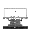
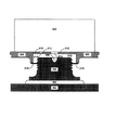
FIG. 2 is a cross-sectional view of an exemplary embodiment of a heat sink including three threaded pedestals according to the present invention. One example embodiment of the present invention utilizes a plurality of thermally conductive threaded pedestals in a single heat sink to allow heat dissipation from a plurality of non-coplanar top heating electronic devices. Can be. In the example embodiment of the present invention shown in FIG. 2, three differently-heated electrical devices are thermally coupled to a single heat sink body 220 and a single set of
第1のハンダ空洞222、第2のハンダ空洞228、及び、第3のハンダ空洞234を含む、ヒート・シンク本体220が製作される。第1のペデスタル204を収容するサイズを付与された開口部248を含む、第1の薄いプレート242が、第1のハンダ空洞222の下においてヒート・シンク本体220に取り付けられている。第2のペデスタル210を収容するサイズを付与された開口部250を含む、第2の薄いプレート244が、第2のハンダ空洞228の下においてヒート・シンク本体220に取り付けられている。第3のペデスタル216を収容するサイズを付与された開口部252を含む、第3の薄いプレート246が、第3のハンダ空洞234の下においてヒート・シンク本体220に取り付けられている。第1のハンダ・オーバフロー・ベント226及び第1の駆動アクセス・ホール224が、第1のハンダ空洞222の上方において、ヒート・シンク本体220の一部に含まれている。第2のハンダ・オーバフロー・ベント232及び第2の駆動アクセス・ホール230が、第2のハンダ空洞228の上方において、ヒート・シンク本体220の一部に含まれている。第3のハンダ・オーバフロー・ベント238及び第2の駆動アクセス・ホール236が、第3のハンダ空洞234の上方において、ヒート・シンク本体220の一部に含まれている。第1の駆動ソケット206を含む第1のネジ付きペデスタル204、第2の駆動ソケット212を含む第2のネジ付きペデスタル210、及び、第3の駆動ソケット218を含む第3のネジ付きペデスタル216が、設けられている。
ヒ ー ト The heat sink body 220 including the
図2に示す本発明の実施態様例を利用する場合、3つの駆動アクセス・ホール224、230、及び、236を通る駆動ツール(ドライバー等のドライブツール)によって、高さの異なる3つの発熱電気デバイス202、208、及び、214に合わせて、3つのネジ付きペデスタル204、210、及び、216の高さ等が調整される。本発明の他の実施態様では、駆動ソケット及び駆動アクセス・ホールの利用を必要としないこともある。組立てられたヒート・シンクが基板上に配置される前に、ヒート・シンクにネジ付きペデスタルを既知の深さまでねじ込むこと(螺合すること)によって、駆動ソケット及び駆動アクセス・ホールの必要がなくなる。3つの発熱電気デバイス202、208、及び、214と3つのネジ付きペデスタル204、210、及び、216との間に、ハンダ・ペースト、熱グリース、または、熱パッドといった熱伝導性材料を用いることが可能である。3つのハンダ空洞222、228、及び、234を溶融ハンダで充填して、3つのネジ付きペデスタル204、210、及び、216とヒート・シンク本体220との間で低い抵抗を有する熱接続を構成することが可能である。3つのハンダ空洞222、228、及び、236の充填は、基板200に対するヒート・シンクの機械的取り付け前または後に実施可能である。ハンダ空洞222、228、及び、236の充填時に、過剰なハンダが、3つのハンダ・オーバフロー・ベント226、232、及び、238を介して漏れ出す可能性がある。3つのハンダ・オーバフロー・ベント226、232、及び、238におけるハンダの存在は、3つのハンダ空洞222、228、及び、236が満杯であることの視覚的表示として利用することが可能である。
When utilizing the exemplary embodiment of the present invention shown in FIG. 2, three heat generating electrical devices having different heights by a driving tool (a driving tool such as a driver) passing through three
図3は、本発明によるヒート・シンクの代替実施態様例に関する断面図である。本発明の実施態様の中には、ヒート・シンク本体308とヒート・シンク・フィン320の間にプレート312を取り付けることによって、ヒート・シンク本体308を単純化するのが望ましいものもあり得る。本発明の実施態様には、ヒート・シンク・ベース308、プレート312、及び、フィン320を個別に製作して、ヒート・シンクをなすように組立てるのではなく、全て、ヒート・シンクの一体化部品として製作することが可能なものもある点に留意されたい。この実施態様の場合、ハンダ・オーバフロー・ベント316及び駆動アクセス・ホール314は、ヒート・シンク本体308内にではなく、プレート312に形成することが可能である。薄いプレート310が、ハンダ空洞318の下においてヒート・シンク本体308の底面に取り付けられている。発熱電気デバイス300が、基板302に取り付けられ、駆動ソケット306を含む熱伝導性ネジ付きペデスタル304が、薄いプレート310にねじ込まれている。プレート312の追加以外については、本発明のこの実施態様例は、図1に示すものと同様である。
FIG. 3 is a cross-sectional view of an alternative embodiment of a heat sink according to the present invention. In some embodiments of the present invention, it may be desirable to simplify the
図4は、本発明によるヒート・シンクの実施態様例に関する平面図である。断面Aは、図1及び図3に用いられている断面である。図2に示す本発明の実施態様と同様、ヒート・シンク本体408に取り付けられたヒート・シンク・フィン400が示されている。図1及び図3に示す本発明の実施態様例の場合には、図4のヒート・シンク本体408は、プレートを示すことになる。ヒート・シンク本体408には、ハンダ・オーバフロー・ベント406及び駆動アクセス・ホール402が示されている。駆動ソケット404は、駆動アクセス・ホール402から見ることができる。
FIG. 4 is a plan view of an embodiment of the heat sink according to the present invention. Section A is the section used in FIGS. 1 and 3. A
図5は、本発明によるヒート・シンクを製作する方法例のフローチャートである。ステップ500では、ハンダ空洞を含むヒート・シンク本体が設けられる。オプションのステップ502では、ヒート・シンク本体にヒート・シンク・フィンが取り付けられる。本発明の他の実施態様例では、ヒート・シンク・フィンは、ヒート・シンク本体の一体化部分として形成することもできるし、あるいは、全く必要としない場合もある。ステップ504では、ヒート・シンク本体に、ハンダ空洞内へのオーバフロー・ベントが形成される。オプションのステップ506では、ヒート・シンク本体に、ハンダ空洞内への駆動アクセス・ホールが形成される。ステップ508では、熱伝導性ペデスタルを収容するサイズが付与された開口部を含む薄いプレートが、ハンダ空洞の下においてヒート・シンク本体に機械的に取り付けられる。ステップ510では、熱伝導性ペデスタルが薄いプレートの開口部にねじ込まれる。ステップ512では、ペデスタルの底面の位置が、基板上の発熱電気デバイスの高さに一致するように調整される、つまりペデスタルの底面が基板上の発熱電気デバイスに接するように調整される。ステップ514では、ハンダ空洞に溶融ハンダが充填される。オプションのステップ516では、熱ペデスタルと電気デバイスの間に、熱ペーストのような熱伝導材料が配置される。オプションのステップ518では、ヒート・シンク・アセンブリが、基板に機械的に取り付けられる。本発明の実施態様によっては、ヒート・シンク本体を基板に機械的に取り付ける必要のないものもある。そうした実施態様では、本発明の範囲内において、他の技法を利用することにより、ヒート・シンクのシフトを阻止することが可能である。さらに、本発明の他の実施態様には、溶融ハンダでハンダ空洞を充填する前に、ヒート・シンク・アセンブリを基板に取り付けることが可能なものもある。
FIG. 5 is a flowchart of an example of a method for manufacturing a heat sink according to the present invention. In
図6は、本発明によるヒート・シンクの実施態様例に関する断面図である。発熱電子デバイス600が基板602に取り付けられている。歯付きの熱伝導性ペデスタル604が、基板602の反対側にある電子デバイス600と熱的に結合されている。歯付きペデスタル604は、螺旋状のネジ山の代わりに、ペデスタルの外周に一連の円形の鋸歯状切り込みを備えている。ヒート・シンク・ベース608、プレート612、フィン620、及び、薄いプレート610を含むヒート・シンクが、プッシュ・イン・ペデスタル604に取り付けられている。組立て時には、歯付きペデスタル604は、薄いプレート610の適切なサイズを付与された開口部にただ単に押し込まれるだけであり、歯付きペデスタル604表面の鋸歯によって、ヒート・シンクから戻されて、外れるのが阻止される。図6に示す歯は、例示のため、サイズが誇張されているという点に留意されたい。本発明の多くの実施態様では、この図に示すものと比べて、つり合いのとれた小さい歯が利用されている。薄いプレート610は、歯付きペデスタル604をぴったりとはめることができるように構成されているが、さらに、歯付きペデスタル604を角度をつけてプレートにはめることができるようにも構成されているので、薄いプレート610に対して平行ではない発熱デバイス600に対して利用することが可能になる。本発明の実施態様の中には、図2に示すように、プレート612をヒート・シンク・ベース608の連続部分として形成することが可能なものもある。本発明の他の実施態様には、ヒート・シンク・ベース608とは別個にプレート612を製作し、互いに物理的に接続することによって、図6に示す、ヒート・シンク・フィン620の取り付け面を形成することが可能なものもある。プレート612には、駆動アクセス・ホール614及びハンダ・オーバフロー・ベント616が含まれている。プッシュ・イン・ペデスタル604には、駆動ソケット606が含まれている。
FIG. 6 is a cross-sectional view of an embodiment of the heat sink according to the present invention. The heat-generating
本発明の以上の説明は、例証及び解説を目的として提示されたものである。本発明を余すところなく説明しようとか、あるいは、開示の形態にそっくりそのまま制限することを意図したものではなく、上記教示に鑑みて、他の修正及び変更を加えることが可能である。実施態様は、本発明の原理、及び、その実際の応用例を最も分りやすく説明することによって、他の当業者が、企図する特定の用途に合わせた、さまざまな実施態様及びさまざまな修正態様において、本発明を最も有効に利用できるように、選択され、解説されている。先行技術による制限のある場合を除いて、付属の請求項は、本発明の他の代替実施態様を含むものと解釈されるように意図されている。 The foregoing description of the present invention has been presented for purposes of illustration and description. It is not intended to be exhaustive or to limit the invention to the precise form disclosed, and other modifications and changes may be made in light of the above teachings. The embodiments will best explain the principles of the invention and its practical applications, and will enable others skilled in the art to review various embodiments and various modifications that are tailored to the particular application contemplated. It has been selected and described in order to make the most effective use of the present invention. Except as limited by the prior art, the appended claims are intended to be construed to include other alternative embodiments of the invention.
本発明は、基板上で使用される電子部品に対するヒートシンクにおいて利用可能である。 The present invention can be used in a heat sink for electronic components used on a substrate.
100 電気デバイス
102 基板
104 ペデスタル
106 駆動ソケット
108 ヒート・シンク本体
110 薄いプレート
112 プレート
114 駆動アクセス・ホール
116 オーバフロー・ベント
118 空洞
604 ペデスタル
610 薄いプレート
REFERENCE SIGNS
Claims (10)
空洞を含むヒート・シンク本体と、
前記ヒート・シンク本体に機械的に取り付けられて、前記空洞を覆い、かつ開口部を含む薄いプレートと、
前記薄いプレートの開口部に挿入されるペデスタルが含まれている、
ヒート・シンク。 A heat sink,
A heat sink body including a cavity,
A thin plate mechanically attached to the heat sink body, covering the cavity, and including an opening;
A pedestal inserted into the opening of the thin plate;
heatsink.
前記ヒート・シンク本体は、前記ヒート・シンク本体を介して、前記ペデスタルの駆動ソケットへのアクセスを可能にするように構成された、前記空洞内へつながる駆動アクセス・ホールを含むことを特徴とする、
請求項1に記載のヒート・シンク。 The pedestal has a drive socket;
The heat sink body includes a drive access hole leading into the cavity configured to allow access to the drive socket of the pedestal through the heat sink body. ,
The heat sink according to claim 1.
空洞を含むヒート・シンク本体と、
前記ヒート・シンク本体に機械的に取り付けられたプレートと、
前記ヒート・シンク本体に機械的に取り付けられて、前記空洞を覆い、かつ開口部を含む薄いプレートと、
前記薄いプレートの開口部に挿入されるペデスタルが含まれている、
ヒート・シンク。 A heat sink,
A heat sink body including a cavity,
A plate mechanically attached to the heat sink body,
A thin plate mechanically attached to the heat sink body, covering the cavity, and including an opening;
A pedestal inserted into the opening of the thin plate;
heatsink.
前記プレートは、前記プレートを介して、前記ペデスタルの駆動ソケットへのアクセスを可能にするように構成された、前記空洞内へつながる駆動アクセス・ホールを含むことを特徴とする、
請求項5に記載のヒート・シンク。 The pedestal has a drive socket;
The plate includes a drive access hole leading into the cavity configured to allow access to the drive socket of the pedestal through the plate.
A heat sink according to claim 5.
a)空洞を含むヒート・シンク本体を設けるステップと、
b)前記ヒート・シンク本体に前記空洞内へつながるオーバフロー・ベントを形成するステップと、
c)前記空洞の下方において、前記ヒート・シンク本体に開口部を含む薄いプレートを取り付けるステップと、
d)前記薄いプレートの開口部にペデスタルを挿入するステップが含まれている、
方法。 A method for configuring a heat sink, comprising:
a) providing a heat sink body including a cavity;
b) forming an overflow vent in the heat sink body leading into the cavity;
c) attaching a thin plate including an opening to the heat sink body below the cavity;
d) inserting a pedestal into the opening of the thin plate;
Method.
e)電気デバイスの高さと一致するように前記ペデスタルを調整するステップと、
f)前記空洞を溶融ハンダで充填するステップと、
g)前記ヒート・シンクを基板に機械的に取り付けるステップが含まれていることを特徴とする、
請求項9に記載のヒート・シンクを構成するための方法。 further,
e) adjusting the pedestal to match the height of the electrical device;
f) filling the cavity with molten solder;
g) mechanically attaching the heat sink to a substrate.
A method for configuring a heat sink according to claim 9.
Applications Claiming Priority (1)
| Application Number | Priority Date | Filing Date | Title |
|---|---|---|---|
| US10/209,981 US6695042B1 (en) | 2002-07-31 | 2002-07-31 | Adjustable pedestal thermal interface |
Publications (2)
| Publication Number | Publication Date |
|---|---|
| JP2004072106A true JP2004072106A (en) | 2004-03-04 |
| JP2004072106A5 JP2004072106A5 (en) | 2005-06-02 |
Family
ID=31187183
Family Applications (1)
| Application Number | Title | Priority Date | Filing Date |
|---|---|---|---|
| JP2003281055A Pending JP2004072106A (en) | 2002-07-31 | 2003-07-28 | Adjustable pedestal thermal interface |
Country Status (3)
| Country | Link |
|---|---|
| US (1) | US6695042B1 (en) |
| JP (1) | JP2004072106A (en) |
| TW (1) | TWI272053B (en) |
Cited By (1)
| Publication number | Priority date | Publication date | Assignee | Title |
|---|---|---|---|---|
| US7577001B2 (en) | 2006-01-16 | 2009-08-18 | Samsung Electronics Co., Ltd. | Support structure of electronic device and hard disk drive comprising the same |
Families Citing this family (16)
| Publication number | Priority date | Publication date | Assignee | Title |
|---|---|---|---|---|
| US7288839B2 (en) * | 2004-02-27 | 2007-10-30 | International Business Machines Corporation | Apparatus and methods for cooling semiconductor integrated circuit package structures |
| US7257001B2 (en) * | 2004-04-23 | 2007-08-14 | Shmuel Erez | Device and method for fastener-free connection via a heat-shrinkable insert |
| FR2886809B1 (en) * | 2005-06-03 | 2007-08-10 | Thales Sa | THERMAL DRAIN FOR ELECTRONIC CARD |
| US7277291B2 (en) * | 2005-08-08 | 2007-10-02 | Verifone Holdings, Inc. | Thermal transfer device |
| US7905276B2 (en) * | 2006-02-09 | 2011-03-15 | Onscreen Technology, Inc. | Method and apparatus for leak-proof mounting of a liquid cooling device on an integrated circuit |
| US20080173427A1 (en) * | 2007-01-23 | 2008-07-24 | Richard Schumacher | Electronic component cooling |
| US20100008045A1 (en) * | 2008-07-09 | 2010-01-14 | Hong Fu Jin Precision Industry(Shenzhen) Co., Ltd | Heat sink |
| US8018719B2 (en) * | 2009-05-26 | 2011-09-13 | International Business Machines Corporation | Vapor chamber heat sink with cross member and protruding boss |
| WO2015012790A1 (en) * | 2013-07-22 | 2015-01-29 | Ge Intelligent Platforms, Inc. | Square plug adjustable heat sinks and methods of fabricating the same |
| WO2015012792A1 (en) * | 2013-07-22 | 2015-01-29 | Ge Intelligent Platforms, Inc. | Screw plug adjustable heat sinks and methods of fabricating the same |
| US9736966B1 (en) * | 2016-02-10 | 2017-08-15 | International Business Machines Corporation | Heat sink with integrated threaded lid |
| US10182514B2 (en) | 2016-06-27 | 2019-01-15 | International Business Machines Corporation | Thermal interface material structures |
| CN106852073B (en) * | 2017-01-13 | 2019-06-07 | 奇鋐科技股份有限公司 | Heat radiation module |
| CN108260325B (en) * | 2017-12-04 | 2024-02-06 | 国网新疆电力公司吐鲁番供电公司 | Water-cooling heat dissipation device |
| US11262815B2 (en) * | 2019-11-01 | 2022-03-01 | Hewlett Packard Enterprise Development Lp | Heat sink system with broad compatibility capacity |
| US11908495B2 (en) | 2022-04-21 | 2024-02-20 | Western Digital Technologies, Inc. | Electronic device with heat transfer pedestal having optimized interface surface and associated methods |
Family Cites Families (9)
| Publication number | Priority date | Publication date | Assignee | Title |
|---|---|---|---|---|
| US2993153A (en) * | 1958-09-25 | 1961-07-18 | Westinghouse Electric Corp | Seal |
| US3170098A (en) * | 1963-03-15 | 1965-02-16 | Westinghouse Electric Corp | Compression contacted semiconductor devices |
| US3313987A (en) * | 1964-04-22 | 1967-04-11 | Int Rectifier Corp | Compression bonded semiconductor device |
| DE1764795A1 (en) * | 1968-01-12 | 1971-11-11 | Siemens Ag | Rectifier arrangement |
| DE2042333A1 (en) * | 1970-08-26 | 1972-03-02 | Siemens Ag | Method for gas-tight sealing of semiconductor components |
| JPH1070219A (en) * | 1996-08-27 | 1998-03-10 | Fujitsu Ltd | Packaged module cooling device |
| US6014315A (en) * | 1998-09-08 | 2000-01-11 | Chip Coolers, Inc. | Heat sink assembly with multiple pressure capability |
| US5945736A (en) * | 1998-09-28 | 1999-08-31 | Chip Coolers, Inc. | Heat sink assembly with snap-in cover plate having multiple pressure capability |
| US6021045A (en) * | 1998-10-26 | 2000-02-01 | Chip Coolers, Inc. | Heat sink assembly with threaded collar and multiple pressure capability |
-
2002
- 2002-07-31 US US10/209,981 patent/US6695042B1/en not_active Expired - Fee Related
-
2003
- 2003-02-11 TW TW092102788A patent/TWI272053B/en not_active IP Right Cessation
- 2003-07-28 JP JP2003281055A patent/JP2004072106A/en active Pending
Cited By (1)
| Publication number | Priority date | Publication date | Assignee | Title |
|---|---|---|---|---|
| US7577001B2 (en) | 2006-01-16 | 2009-08-18 | Samsung Electronics Co., Ltd. | Support structure of electronic device and hard disk drive comprising the same |
Also Published As
| Publication number | Publication date |
|---|---|
| US6695042B1 (en) | 2004-02-24 |
| TWI272053B (en) | 2007-01-21 |
| US20040020634A1 (en) | 2004-02-05 |
| TW200402260A (en) | 2004-02-01 |
Similar Documents
| Publication | Publication Date | Title |
|---|---|---|
| JP2004072106A (en) | Adjustable pedestal thermal interface | |
| US5920458A (en) | Enhanced cooling of a heat dissipating circuit element | |
| KR100523498B1 (en) | Parallel-plate/pin-fin hybrid copper heat sink for cooling high-powered microprocessor | |
| US6180436B1 (en) | Method for removing heat from a flip chip semiconductor device | |
| US5792677A (en) | Embedded metal planes for thermal management | |
| US20060061969A1 (en) | Circuit arrangement for cooling of surface mounted semi-conductors | |
| US6821816B1 (en) | Relaxed tolerance flip chip assembly | |
| US20030139071A1 (en) | Thermally enhanced interposer and method | |
| JP2009044156A (en) | Circuit support structure having improved radiation property | |
| JP2004095586A (en) | Electric apparatus and wiring board | |
| US20180241285A1 (en) | Cooling a heat-generating electronic device | |
| WO1981003734A1 (en) | Heat pin integrated circuit packaging | |
| JP6569314B2 (en) | Substrate heat dissipation structure and assembly method thereof | |
| JP2020533796A (en) | Printed circuit board with heat sink | |
| CN111615746A (en) | Power electronic module and method of manufacturing a power electronic module | |
| JP3733783B2 (en) | Module having heat dissipation structure of heating element | |
| JP2006332479A (en) | Power semiconductor device | |
| US6625026B1 (en) | Heat-activated self-aligning heat sink | |
| JP2010205863A (en) | On-vehicle electronic controller | |
| JP2004247684A (en) | Heat sink and heat radiating device | |
| JP2007019125A (en) | Electric power conversion device | |
| CN109075241B (en) | Thermal block assembly, LED arrangement with thermal block assembly and method of manufacturing the thermal assembly | |
| US20050199377A1 (en) | Heat dissipation module with heat pipes | |
| JP3378174B2 (en) | Heat dissipation structure of high heating element | |
| CN210298190U (en) | PCB structure easy to radiate heat |
Legal Events
| Date | Code | Title | Description |
|---|---|---|---|
| A521 | Written amendment |
Free format text: JAPANESE INTERMEDIATE CODE: A523 Effective date: 20041008 |
|
| A621 | Written request for application examination |
Free format text: JAPANESE INTERMEDIATE CODE: A621 Effective date: 20041008 |
|
| A131 | Notification of reasons for refusal |
Free format text: JAPANESE INTERMEDIATE CODE: A131 Effective date: 20070925 |
|
| A02 | Decision of refusal |
Free format text: JAPANESE INTERMEDIATE CODE: A02 Effective date: 20080304 |