JP2004030884A - Method to minimize error in magnetoresistive solid-state storage device - Google Patents
Method to minimize error in magnetoresistive solid-state storage device Download PDFInfo
- Publication number
- JP2004030884A JP2004030884A JP2003126443A JP2003126443A JP2004030884A JP 2004030884 A JP2004030884 A JP 2004030884A JP 2003126443 A JP2003126443 A JP 2003126443A JP 2003126443 A JP2003126443 A JP 2003126443A JP 2004030884 A JP2004030884 A JP 2004030884A
- Authority
- JP
- Japan
- Prior art keywords
- cells
- cell
- tendency
- parallel
- group
- Prior art date
- Legal status (The legal status is an assumption and is not a legal conclusion. Google has not performed a legal analysis and makes no representation as to the accuracy of the status listed.)
- Pending
Links
Images


Classifications
-
- G—PHYSICS
- G11—INFORMATION STORAGE
- G11C—STATIC STORES
- G11C11/00—Digital stores characterised by the use of particular electric or magnetic storage elements; Storage elements therefor
- G11C11/02—Digital stores characterised by the use of particular electric or magnetic storage elements; Storage elements therefor using magnetic elements
- G11C11/14—Digital stores characterised by the use of particular electric or magnetic storage elements; Storage elements therefor using magnetic elements using thin-film elements
- G11C11/15—Digital stores characterised by the use of particular electric or magnetic storage elements; Storage elements therefor using magnetic elements using thin-film elements using multiple magnetic layers
Abstract
Description
【0001】
【発明の属する技術分野】
本発明は、一般に磁気抵抗固体記憶素子に関し、特に磁気抵抗固体記憶素子における誤りを最小限にすることに関する。
【0002】
【従来の技術】
磁気ランダムアクセスメモリ(MRAM)素子といった一般的な磁気抵抗固体記憶素子は、記憶セルのアレイを含む。各セルは典型的には、誘電体層により分離された2つの磁気薄膜層から構成される。その一方の磁気薄膜層の磁化方向は可変であり、一方、他方の磁気薄膜層の磁化方向は、特定の方向に固定され又は「ピン留め」(pinned)される。可変の磁化方向を有する磁気薄膜層は一般に「データ記憶層」と呼ばれ、固定された磁化方向を有する磁気薄膜層は一般に「基準層」と呼ばれる。
【0003】
かかる記憶セルのアレイにわたり複数の導電性トレースが配線される。該導電性トレースは、一般に行及び列に配列される。記憶セルの行に沿って延びる導電性トレースは一般に「ワード線」と呼ばれ、記憶セルの列に沿って延びる導電性トレースは一般に「ビット線」と呼ばれる。該ワード線及びビット線は、一般に互いに垂直に向けられる。各記憶セルは、ワード線とビット線との各交点に配置され、1つの磁化方向として1ビットの情報を格納する。
【0004】
一般に、データ記憶層内の磁化方向は、データ記憶層の軸(一般に磁化容易軸と呼ばれる)に沿って整列する。一般に、所望の論理状態に応じて、磁化容易軸に沿ったデータ記憶層内の磁化方向を基準層内の磁化方向に対して平行又は逆平行の何れかの方向に反転させるように、外部磁界がかけられる。
【0005】
各記憶セルの磁化方向は、あらゆる所与の時点で2つの安定した方向のうちの一方を呈することになる。一般に、これらの2つの安定した方向、すなわち平行及び逆平行は「1」及び「0」の論理値をそれぞれ表すものとなる。代替的に、逆平行状態を論理「1」と解釈し、平行状態を論理「0」と解釈するようシステムを構成することも可能である。選択された記憶セルの磁化方向は、該選択された記憶セルの位置で交差するワード線とビット線とに電流を供給することにより変更する(すなわち、平行から逆平行に又はその逆にする)ことが可能である。該電流は磁界を生成し、該磁界が組み合わされて、選択された記憶セルの磁化方向を平行から逆平行に(又はその逆に)切り替えることが可能となる。
【0006】
理想的には、MRAMアレイの各セル内の磁界は、平行又は逆平行の何れかの方向に整列することになる。しかし、残念ながら、MRAMアレイを形成するために用いられる磁性材料の不完全性に起因して、MRAMアレイ内の各セルは完全には直角に配置されない場合がある。それ故、記憶セルのうちの幾つかの磁界が互いに整列しなくなる場合がある。かかるセルの磁界は、一般に、逆平行又は平行の何れかの方向に整列しやすい傾向を有するものとなり、その結果として、該セルにデータを書き込もうとする際に誤りが生じる可能性がある。状況によっては、特定のセル内の磁界が逆平行又は平行の何れかの方向に固定されてしまうことすらある。一方の方向を他の方向よりも好む傾向を有するセルは一般に、書き込みが行われる際にその方向を確実に切り替えないため、データに誤りが導入されることになる。例えば、MRAMアレイ内に2進数0000を格納したいものと仮定する。しかし、2進数0000の各ビットがアレイ内の各セルに書き込まれ、それらのビットのうちの1つが、論理「1」に対応する磁化方向に留まる傾向を有するセルに書き込まれる場合には、書き込まれた数がアレイから読み出される際に、論理「1」に対応する磁化方向に留まる傾向を有するセルから「0」でなく「1」が読み出され(例えば、該アレイから読み出される数が0000ではなく0010になる可能性があり)、このため、システム内に誤りが生じることになる。
【0007】
【発明が解決しようとする課題】
それ故、本発明の目的は、MRAM素子における上記の欠陥及び欠点を解消させることにある。
【0008】
【課題を解決するための手段】
本発明は、磁気ランダムアクセスメモリ(MRAM)素子アレイといった複数のセルを有する磁気抵抗固体記憶素子における誤りを最小限にすることを可能にする例示的な実施形態を提供する。本開示の方法は、特定の磁化方向に留まる傾向を有することを特徴とする故障挙動(failure mode)を有する磁気抵抗固体記憶素子内のセルを識別し、該識別されたセルの場所をマッピングし、該マッピングされた場所においてセルの故障挙動を補償する、という各ステップを含むことを特徴とするものである。
【0009】
1つの例示的なシステムは、特定の磁化方向に留まる傾向を有することを特徴とする故障挙動を有する磁気抵抗固体記憶素子内のセルを識別するよう構成された検査要素と、メモリ要素と、前記識別されたセルの場所を前記メモリ要素内にマッピングして該マッピングされたセルの故障挙動を補償するよう構成された処理要素とを含む。
【0010】
本発明の他の特徴及び利点は、以下の図面及び詳細な説明を検討することにより当業者には明らかとなろう。全てのかかる特徴及び利点は、特許請求の範囲により規定される本発明の範囲内に含めることが意図されたものである。
【0011】
【発明の実施の形態】
特許請求の範囲で規定する本発明は、図面を参照して一層良好に理解することが可能である。同図面における各構成要素は必ずしも互いに対して縮尺が一定である訳ではなく、本発明の原理を明瞭に示すことに重きがおかれている。
【0012】
本発明の以下に記載する詳細な説明では、その一部を形成し、一例として本発明が実施され得る特定の実施形態を示す、図面への参照がなされる。他の実施形態が用いられてもよく、本発明の範囲から逸脱することなく、構造的又は論理的な変更がなされ得ることを理解されたい。それ故、以下に記載される詳細な説明は、本発明を限定する意味に受け取られるべきではなく、本発明の範囲は、特許請求の範囲により規定される。例えば、以下の説明では、本発明を磁気ランダムアクセスメモリ(MRAM)アレイに適用されるものとして説明するが、本発明は一般に、MRAM、EEPROM、フリップフロップ、シフトレジスタ等(但しこれらには限定されない)を含む、磁気抵抗記憶セルを記憶要素として用いる任意の素子に適用することが可能である。
【0013】
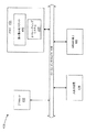
ここで図面を参照する。同図では、類似する参照符号は幾つかの図面を通して対応する構成要素を示している。図1は、本発明の実施形態が動作することが可能な例示的な磁気抵抗固体記憶素子である磁気ランダムアクセスメモリ(MRAM)素子アレイを単純化して示す説明図である。同図は、制御回路118に接続された記憶セル116のアレイ110を含むMRAM素子100を単純化して示している。
【0014】
典型的な実施形態では、MRAM素子100は約1024×1024の記憶セルを含むが、それよりも遙かに少数の記憶セルを有する例を図示している。記憶セル116はそれぞれ制御線112,114の交点に形成される。この例では、制御線112は行をなすよう配列され、制御線114は列をなすよう配列されている。制御線112,114は典型的には直交するが、他の更に複雑な格子構造も実施可能である。好適には、行線112及び列線114は制御回路118に接続され、該制御回路118は複数の読み出し/書き込み制御回路を含むものとなる。実装形態に応じて、一列につき1つの読み出し/書き込み制御回路が設けられ、又は複数列間で読み出し/書き込み制御回路が多重化されもしくは共有される。
【0015】
書き込み動作又は読み出し動作といった素子へのアクセス時には、図1に示すように、必要とされる1つ又は2つ以上の記憶セル116にアクセスするために、典型的には1つの行112と1つ又は2つ以上の列114とが制御回路118により選択される。しかし、アレイ110の方向に応じて、1つの列114と複数の行112とを制御回路118により選択することが可能である。図1に示す例示的な構成を参照すると、選択されたセル116、選択された行線112、及び選択された列線114はそれぞれ太線により表されている。典型的なMRAM素子は、セル間の干渉を最小限にするために、選択された列線114間に最小距離m(例えば64セル)を必要とする。各アレイ110が、長さl(例えば1024記憶セル)の行を有する場合には、該アレイ110から一意にアドレス指定することが可能なl/m=1024/64=16個までのセルに同時にアクセスすることが可能である。
【0016】
各記憶セル116は、数値、好適には2進値(すなわち1又は0)を適当に表す1ビットのデータを格納する。好適には、各記憶セルは、平行及び逆平行として知られる2つの安定した磁化方向のうちの一方を呈する2つの薄膜を含むものとなる。該磁化方向は、記憶セルの抵抗値に影響を与えるものとなる。記憶セル116が逆平行状態にある場合に、その抵抗値はその最も高くなり、該記憶セル116が平行状態にある場合には、その抵抗値はその最も低くなる。好適には、高抵抗の逆平行状態が「0」論理状態を画定し、低抵抗値の平行状態が「1」論理状態を画定する(その逆も可能である)。磁気抵抗固体記憶素子の1つの典型的な実施形態では、各記憶セル116の抵抗値は、スピントンネル現象として知られる現象にしたがって決定され、該記憶セルは、磁気トンネル接合記憶セルと呼ばれる。記憶セルの状態は、センス電流(抵抗値に比例する)、又は既知のキャパシタンスを放電するための応答時間といった関連するパラメータを測定し、各記憶セル毎に1つ又は2つ以上のパラメータ値を取得することにより求められる。次いで、取得された1つ又は2つ以上のパラメータ値から論理値を導出することができる。MRAM素子の特性及び構成に応じて、読み出し動作は、複数ステップを含むことが可能であり、又は読み出し及び再書き込み動作の組み合わせを必要とすることが可能である。
【0017】
図2は、図1のMRAM素子100を更に詳細に示したものである。複数の個々のアレイ110を含むマクロアレイ200が形成され、その各アレイ110は、図1に関して上述したように形成される(単純化のため制御回路118を図2から省略した)。複数のアレイを利用することにより、アレイ内の個々のアレイ110をその製造又は制御が困難になるほど大きくすることなく、所望の全データ記憶容量を有するMRAM素子を得ることが可能となる。単純化のため、図2はマクロアレイ200の一部のみを示している。
【0018】
素子の製造中に適当な基板上にアレイ110をレイアウトする際には、当業者であれば数多くの設計上の選択が可能であるが、とりわけ、各アレイのための基板面積を縮小させることが一般に望ましい。都合のよいことに、アレイ110を複数の層として製造できることがわかった。図2の例では、4つのアレイ110が積層化されて1つのスタック115が形成される。144Mb程度の記憶容量を有する一例の実際的な素子の場合には、1152個のアレイ110が、4つのスタック層を有する幅16アレイ×高さ18アレイのマクロアレイとして配列される。随意選択的に、MRAM素子は2つ以上のかかるマクロアレイを含むことが可能である。
【0019】
図2に示すように、マクロアレイ200に対するアクセスは、複数のアレイ110の各々における1つの行112を選択し及び該複数のアレイの各々から複数の列114を選択することで複数の記憶セル116(図1)を選択することにより、行うことが可能である。複数のアレイの各々におけるアクセスされるセルは、一単位のデータの小部分に対応する。アクセスされるセルが共に一つになって、一単位のデータ全体(例えば1セクタのデータ全体)又は一単位のデータの少なくとも大部分が提供される。複数のアレイの各々にほぼ同時にアクセスできることが有利であり、これは当業界では「マクロアレイのスライス・スルー(a slice through themacro−array)」として知られている。スライス・スルーを用いることにより、読み出し動作又は書き込み動作に関する素子のアクセス速度が高められる。
【0020】
図2に示すように、複数のアレイ110の各々において同じ行アドレス及び同じ列アドレスを選択するのが好適である。すなわち、一単位のデータは、複数のアレイ110の各々において同じ行及び列アドレスを用いて複数のアレイ110にわたって格納される。
【0021】
また図2に示すように、アレイ110は典型的には積層化されてスタックが形成される。一度に各スタック内の1つのアレイにのみアクセスすることができる。それ故、1セクタ単位のデータを格納するために用いられる複数のアレイ110はそれぞれ異なるスタック内に存在する(すなわち選択された複数のアレイはその何れも同じスタック内には存在しない)のが好適である。また、全て同じ層内に存在するアレイを選択するのが好適である。理想的には、各スタックから1つずつアレイが選択され、該アレイの各々が各スタック内の同じ層内に存在する。図2に示す例では、各スタック内の最上位のアレイが選択されている。
【0022】
最も好適には、マクロアレイ200において利用可能なアレイの数が、その素子内に格納されることになる1セクタ単位のデータのサイズと一致することである。この場合には、1つのアレイ内で同時にアクセスできるセルの数が与えられた際に、素子の単一の層のアレイの全てのセルを使用して1セクタ単位を格納して、1セクタ単位のデータ全体を格納するように、アレイの総数を与えるのが好適である。別の実施形態では、1セクタ単位のデータの整数の分の一(例えば1セクタ単位の1/2又は1/3)に同時にアクセスするのが好適となる。
【0023】
概ね信頼性は高いが、素子が記憶セル116にデータを確実に格納するための能力に影響を与える故障が生じ得ることが分かった。故障は、極めて望ましくなく、素子内の少なくとも幾つかの記憶セルに対して確実に書き込み又は読み出しを行うことができないことを意味する。故障による影響を受けるセルは、読み出し不能になって該セルから論理値を読み出すことができなくなり、又は信頼性がなくなって該セルから読み出される論理値が必ずしも該セルに書き込まれた値と同じでなくなる(例えば「1」を書き込んだのに「0」が読み出される)。素子の記憶容量及び信頼性が深刻な影響を受け、最悪の場合には素子全体が使用不能になる可能性がある。
【0024】
故障のメカニズムは数多くの形をとり得るものである。本発明の一実施形態は、セルに異なる状態を書き込もうとしているにもかかわらず該セルが通常の動作時に平行又は逆平行の何れかの状態に留まる傾向を有する結果として生じる誤りを最小限にすることに向けられる。本書で用いるように、セルが特定の状態に留まる傾向は、セルの抵抗値がアレイ内の典型的なセルの抵抗値よりも極めて高いい状況又は極めて低い状況、並びにセルが特定の方向に固定される状況を含む。セルの抵抗値がアレイ内の典型的なセルの抵抗値よりも極めて極めて低い場合には(一般に「短絡ビット」と呼ばれる)、該セルは典型的には、セルを逆平行状態に反転させるために一般に必要とされる電圧よりも高いバイアス電圧において平行状態に留まることになる。また、セルの抵抗がアレイ内の典型的なセルの抵抗よりも極めて高い場合には(一般に「開放ビット」と呼ばれる)、該セルは典型的には、セルを逆平行状態に反転させるために一般に必要とされる電圧よりも高いバイアス電圧において平行状態に留まることになる。セルが平行方向又は逆平行方向の何れかに拘束される場合には、該セルは、バイアス電圧を増加させた場合であっても書き込み命令に応じてその方向を変更しなくなる。
【0025】
本発明の一実施形態は、平行状態又は逆平行状態の何れかをとる傾向を有するセルを含むメモリセクションにデータを正しく読み書きすることを可能にする。ここで、MRAMアレイ内のセルを検査して、そのセルのうちの何れが(もしあるなら)通常の動作時に平行状態又は逆平行状態の何れかに留まる傾向を有するかを判定するための例示的な方法を、図3を参照して説明する。素子は、該素子内の各セルの検査を介して、また代替的には、セルの行及び/又は列の検査を介して、検査することが可能である、ということに留意されたい。上述の複数の故障挙動のうちの幾つかの結果として、関連する複数グループのセルの故障が生じ得るので(例えば、短絡ビットは典型的には、同じ行及び同じ列に存在する全ての記憶セルに影響を与え、開放ビットは(必ずではないが)同じ行もしくは列又はその両者に存在する全ての記憶セルに影響を与える)、アレイ内の各セルが特定の状態をとる傾向は、そのセルの統計的に有意なサンプルが検査される限り、実際に各セルを個々に検査することなく予測することが可能である。
【0026】
図3は、図1関して上述したアレイと類似したアレイ110の一部を概略的に示したものである。図3では、アレイ110は、検査セル160の行120を含む。好適には、検査セル160は、アレイの残りの部分の記憶セル116と同一に構成される。検査行120はあらゆる適当な場所(アレイ110の上部又は底部又は内部等)に設けることが可能である。典型的には、アレイ110の一行の記憶セル116が、検査行120として機能するよう選択される。検査行は、それ自体が故障のあるセルを含まず他の行内の故障のあるセルによる影響を受ける行となるよう適当に選択される。検査行は、好適には、素子の製造時に決定される。また必要であれば、検査行120は、場合に応じて選択し直し又は移動させることが可能である。
【0027】
都合の良いことに、検査行120内の検査セル160の状態を調べることにより、アレイの他の部分の記憶セル116の状態を正確に予測することが可能であることが分かった。1つの例示として、図3は、アレイ110の一部を示しており、該部分でセル161に短絡ビット故障が生じる。図3の典型的なMRAM素子内の故障の性質に起因して、短絡ビットセル161は、同じ行及び同じ列内に存在する全てのセル(検査行120内の検査セル160中の検査セル162を含む)に影響を与える。それ故、検査セル162は、短絡ビット故障が生じており、該故障が検査セル162が存在する列に影響を与えていることを示す。
【0028】
読み出し動作中に、行線112と1つ又は2つ以上の列線114とが(例えば図1の制御回路118により)駆動されて、図3の太線で示すように、アレイ110内の一組の記憶セル116が選択される。短絡ビットセル161の影響を受けているセル163は、これら選択されたセルの中に存在する。検査セル162の状態を調べることにより、セル163が故障による影響を受けていることを予測することができる。次いで、該予測は、該選択されたセルに関する後続の読み出し動作ステージの改善を可能にする。
【0029】
他の方式を用いて、アレイ内のセルのうちの何れが(もしあるなら)通常の動作時に平行又は逆平行の何れかの状態に留まる傾向を有するかを判定することも可能である。1つの単純な動作モードでは、検査セルを一回だけ検査して、故障(特に短絡ビット故障、開放ビット故障、又は「固定された」ビット)による影響を受けるアレイ110内の列114を判定する。
【0030】
検査セル160の検査は、あらゆる適当な形態をとることが可能である。一実施形態では、各検査セル160に論理「1」といった既知の値が書き込まれる。次いで、該検査セル160から論理値を読み出すことにより該検査セル160が検査される。検査セルのうちの任意のセルが論理値「0」を示す場合には、検査セル160が存在する列114に影響を与える短絡ビット故障等の故障が生じているものと予測することができる。同様に、検査セルに「0」を書き込み「1」が読み出された場合には、開放ビット故障が示されることになる。随意選択的に、2つの検査行を設けることが可能であり、この場合には、第1の検査行は短絡ビット故障を示すよう構成され、第2の検査行は開放ビット故障を示すよう構成される。検査セルは、一回だけ書き込んで繰り返し読み出すことが可能であり、又はセルの保全性を維持するために、必要に応じて各読み出しの後に再び書き込むことが可能である。検査セル160の場所及び性質、並びに検査セル160の検査方法は、特定のMRAM素子の特定の性質に合わせて容易に変更することが可能である。
【0031】
検査セル160を使用してアレイ内のセルの故障挙動を予測することが可能であるが、代替的に、アレイ中の各セルを(例えばバーンイン中に)検査して各セルの故障挙動を判定することが可能である。例えば、平行状態が論理「1」を構成し、逆平行状態が論理「0」を構成するものと仮定する。一実施形態では、アレイ110内の各セルに論理「1」といった既知の値が書き込まれる。セルから論理「0」が読み出された場合には、該セルは逆平行状態をとる傾向を有するものとみなされる。同様に、セルに「0」を書き込み「0」が読み出された場合には、該セルが平行状態をとる傾向を有することが示されることになる。
【0032】
各セルを検査することにより、又は統計的に有意な数の選択された検査セルを検査し、該選択された検査セルの検査結果に基づいて他のセルの傾向を予測することにより、特定の方向をとる傾向を有するセルが識別されると、該傾向を補償する態様でデータがセルに格納される。こうして、本発明は、かかるセルを回避するのではなく、その使用を可能にする。
【0033】
本発明の実施形態は、ソフトウエア(例えばファームウエア)、ハードウエア、又はそれらの組み合わせで実施することが可能である。一例として、そのシステムは、パーソナルコンピュータ(PC;IBM互換機、Apple互換機その他)、ワークステーション、ミニコンピュータ、又はメインフレームコンピュータにおけるプロセッサといった専用又は汎用プロセッサにより実行される実行可能プログラム等のソフトウエアを含むコンピュータシステムにおいて実施することが可能である(但しこれらには限定されない)。本発明の実施形態を実施することができる汎用コンピュータの一例を図4に示す。図4では、コンピュータシステムは、符号400で示されている。
【0034】
一般的に、ハードウエア・アーキテクチャに関しては、図4に示すように、該コンピュータシステム400は、図1に関して上述したように構成されるMRAM素子100を含み、該MRAM素子は、本発明の実施形態を実施することが望ましい典型的な磁気抵抗固体記憶素子である。該コンピュータシステム400はまた、プロセッサ412と、メモリ414と、1つ又は2つ以上の入出力(I/O)装置416(又は周辺装置)を含み、それらは全て、ローカルインタフェイス418を介して通信可能となるよう接続される。該ローカルインタフェイス418は、例えば当業界で知られている1つ又は複数のバスその他の有線又は無線接続とすることが可能なものである(但しそれらには限定されない)。ローカルインタフェイス418は、単純化のため省略してあるが、コントローラ、バッファ(キャッシュ)、ドライバ、リピータ、及び受信機といった、通信を可能にするための更に別の装置を有することが可能である。更に、ローカルインタフェイスは、上記の構成要素間における適当な通信を可能にするためのアドレス接続、制御接続、及び/又はデータ接続を含むことが可能である。
【0035】
プロセッサ412は、ソフトウエア(特にメモリ414に格納されたソフトウエア)を実行するためのハードウエア要素である。プロセッサ412は、あらゆる特注品又は市販品のプロセッサ、すなわち中央演算処理装置(CPU)、コンピュータシステム400に付随する幾つかのプロセッサの中の補助プロセッサ、半導体ベースの(マイクロチップ又はチップセットという形の)マイクロプロセッサ、マクロプロセッサ、又は一般にソフトウエア命令を実行するためのあらゆる素子とすることが可能なものである。適当な市販のマイクロプロセッサの例として、ヒューレット・パッカード社のPA−RISCシリーズマイクロプロセッサ、インテル社の80x86又はPentium(R)シリーズマイクロプロセッサ、IBM社のPowerPCマイクロプロセッサ、サンマイクロシステムズ社のSparcマイクロプロセッサ、又はモトローラ社の68xxxシリーズマイクロプロセッサが挙げられる。
【0036】
メモリ414は、揮発性メモリ要素(例えばランダムアクセスメモリ(DRAM、SRAM、SDRAM等のRAM))又は不揮発性メモリ要素(例えば磁気ランダムアクセスメモリ(MRAM)、ROM、ハードドライブ、テープ、CD−ROM等)の何れか一方、又はそれらの組み合わせを含むことができる。MRAMは不揮発性であるが、他のタイプのRAM(すなわち、DRAM、SRAM、SDRAM等)は揮発性であることに留意されたい。このため、特定の応用形態では、揮発性RAMよりも不揮発性のMRAMを用いる方が有利となる。これは、MRAMアレイにおける誤りを最小限にすることの必要性を更に強調している。MRAM素子100は、メモリ414の外部に存在するものとして図示したが、代替的に、メモリ414の一部を構成することが可能である。
【0037】
メモリ414はまた、電子的、磁気的、光学的、及び/又はその他のタイプの記憶媒体を含むことが可能である。メモリ414は、分散形アーキテクチャを有することができ、この場合には種々の構成要素が互いから離隔して配置されるが、プロセッサ412によりアクセスすることが可能である、という点に留意されたい。
【0038】
メモリ414内のソフトウエアは、1つ又は2つ以上の別個のプログラムを含むことが可能であり、該プログラムの各々は、論理機能を実施するための実行可能命令を順に並べたリストを含むものとなる。図4の例では、メモリ414内のソフトウエアは、誤り最小化ロジック410及び適当なオペレーティングシステム(O/S)422を含む。市販の適当なオペレーティングシステム422の例として、(a)Micosoft社のWindowsオペレーティングシステム、(b)Novell社のNetwareオペレーティングシステム、(c)Apple Computer社のMacintoshオペレーティングシステム、(d)Hewlett−Packard社、Sun Microsystems社、及びAT&T社といった数多くのベンダから購入できるUNIXオペレーティングシステム、(e)インターネット上で容易に入手できるフリーウエアのLINUXオペレーティングシステム、(f)WindRiver Systems社のランタイムVxworksオペレーティングシステム、又は(g)ハンドヘルドコンピュータ又は個人情報端末(PDA)に実装されるようなアプライアンス・ベースのオペレーティングシステム(例えば、Palm Computing社のPalmOS、Microsoft社のWindows CE)が挙げられる(但し、これらには限定されない)。オペレーティングシステム422は、基本的には、誤り最小化ロジック410といった他のコンピュータプログラムの実行を制御し、スケジューリング、入出力制御、ファイル及びデータ管理、メモリ管理、並びに通信制御及びそれに関連するサービスを提供する。
【0039】
誤り最小化ロジック410は、ソースプログラム、実行可能プログラム(オブジェクトコード)、スクリプト、又は実行すべき一組の命令を含む他のあらゆるエンティティとすることが可能である。ソースプログラムの場合には、該ソースプログラムは典型的には、O/S422に関連して適当に動作するように、コンパイラ、アセンブラ、インタープリタ及びその類を介して翻訳されることになり、それらは、メモリ414内に含めることも含めないことも可能である。更に、誤り最小化ロジック410は、(a)データクラス及びメソッドを有するオブジェクト指向プログラミング言語として、又は(b)ルーチン、サブルーチン、及び/又は関数を有するプロシージャプログラミング言語(例えば、C、C++、Pascal、Basic、Fortran、Cobol、Perl、Java、及びAda)として書くことが可能である(但しこれらには限定されない)。
【0040】
I/O装置416は、入力装置、例えば、キーボード、マウス、スキャナ、マイクロフォン等を含むことが可能である(但しこれらには限定されない)。更に、I/O装置416は、出力装置、例えば、プリンタ、ディスプレイ等を含むことが可能である(但しこれらには限定されない)。最後に、I/O装置416は更に、入力及び出力の両方と通信する装置、例えば、変調器/復調器(例えば、他の装置、システム、又はネットワークにアクセスするためのモデム)、無線周波数(RF)その他の送受信器、電話インタフェイス、ブリッジ、ルータ等を含むことが可能である。
【0041】
コンピュータ400がPC、ワークステーション、及びその類である場合には、メモリ414内のソフトウエアは更に、BIOS(basic input output system)(単純化のため省略する)を含む可能性がある。BIOSは、始動時にハードウエアを初期化し及び検査し、O/S422を起動させ、ハードウエアデバイス間のデータ転送をサポートする、一組の基本的なソフトウエアルーチンである。BIOSは、コンピュータ300の起動時に実行できるようROMに格納される。
【0042】
コンピュータ400が動作中である場合に、プロセッサ412は、メモリ414内に格納されているソフトウエアを実行し、該メモリ414との間でデータをやりとりし、及び該ソフトウエアに応じてコンピュータ400の動作を全般的に制御するよう構成される。誤り最小化ロジック410及びO/S422は、それらの全体又は一部(典型的には一部)が、プロセッサ412により読み出され、おそらくは該プロセッサ412内にバッファリングされ、次いで実行される。
【0043】
図4に示すように、誤り最小化ロジック410がソフトウエアで実施される場合には、該誤り最小化ロジック410を、コンピュータによりデータを読み出すことが可能なあらゆる媒体(以下「コンピュータ読出可能媒体」と称す)上に格納して、該コンピュータに関連するシステム又は方法により使用し又はそれらに関連して使用することができるようにすることが可能である点に留意されたい。本書では、コンピュータ読出可能媒体は、コンピュータ関連システム又は方法により使用し又はそれらに関連して使用するためのコンピュータプログラムを収容し又は格納することができる電子的、磁気的、光学的、又はその他の物理的な装置又は手段とすることが可能なものである。誤り最小化ロジック410は、命令実行システム、装置、又はデバイス(例えば、コンピュータベースのシステム、プロセッサを含むシステム、又は命令実行システム、装置、又はデバイスからの命令をフェッチして該命令を実行することができる他のシステム)により使用し、又はそれらに関連して使用するためのあらゆるコンピュータ読出可能媒体で実施することが可能である。本書では、「コンピュータ読出可能媒体」は、命令実行システム、装置、又はデバイスにより使用し又はそれらに関連して使用するためのプログラムを格納し、通信し、伝達し、又は移送することができる、あらゆる手段とすることが可能である。コンピュータ読出可能媒体は、例えば、電子、磁気、光学、電磁気、赤外線、又は半導体を利用したシステム、装置、デバイス、又は伝達媒体とすることが可能である(但しこれらには限定されない)。コンピュータ読出可能媒体の更なる特定の例として、1つ又は2つ以上の配線を有する電気的接続(電子的な一例)、ポータブルコンピュータディスケット(磁気的な一例)、ランダムアクセスメモリ(RAM)(電子的な一例)、リードオンリーメモリ(ROM)(電子的な一例)、消去可能プログラマブルリードオンリーメモリ(EPROM、EEPROM、又はフラッシュメモリ)(電子的な一例)、光ファイバ(光学的な一例)、及びポータブルコンパクトディスク・リードオンリーメモリ(CD−ROM)(光学的な一例)が挙げられる(但しこれらには限定されない)。コンピュータ読出可能媒体は、プログラムが印刷された紙その他の適当な媒体とすることも可能である点に留意されたい。これは、プログラムを、例えば、紙その他の媒体の光学的な走査を介して電子的に捕捉し、次いで必要に応じて適当な態様でコンパイルし、解釈し、又はその他の処理を行って、コンピュータメモリに格納することができるからである。
【0044】
システムがハードウエアで実施される代替的な実施形態では、誤り最小化ロジック410は、当業界で周知の技術、すなわち、複数のデータ信号に関して複数の論理機能を実施する複数の論理ゲートを有する離散的な論理回路(discrete logic circuit)、適当な組み合わせ論理ゲートを有する特定用途向け集積回路(ASIC)、プログラマブルゲートアレイ(PGA)、及びフィールドプログラマブルゲートアレイ(FPGA)等の何れか又はそれらの組み合わせを使用して実施することが可能である。
【0045】
図5は、MRAM素子100等の磁気抵抗固体記憶素子にデータを格納する際の誤りを最小限にするために図4の誤り最小化ロジック410により実施することができる典型的な方法を示すフローチャートである。該フローチャートにおけるプロセスの記述又はブロックは、該プロセスにおける特定の論理機能又はステップを実施するための1つ又は2つ以上の実行可能命令を含むことが可能なコードのモジュール、セグメント、又は一部を表すものであることを理解されたい。また、関連する機能に応じて本書で説明し図示する順序とは異なる順序で(例えば、ほぼ同時に又は逆順で)機能が実行される代替的な実装形態もまた本発明の範囲内に含まれることが、当業者には理解されよう。
【0046】
ブロック501では、誤り最小化ロジック410は、MRAM素子100中の各セルのうち、1つの磁化方向(逆平行よりも平行又はその逆)を他の方向よりも好む傾向を有することを特徴とする故障挙動を有するセル、及び各セルに関する特定の故障挙動とを識別する。図5に示す実施形態では、故障挙動の判定は、誤り最小化ロジック410により行われる。
【0047】
本発明は、アレイ内のセルのうち1つの磁化方向を他の方向よりも好む傾向を有するセルを識別するために使用される特定の方法に限定されるものではない。当業者に知られているあらゆる検査方法(図3に関して上述した典型的な検査方法を含む(但しこれには限定されない))を使用して、素子内のセルの傾向を判定することが可能である。別の考え得る検査方法として(当業者にとって既知であるように)、素子中のセルの幾つか又は全てについてBH曲線を解析することが挙げられる。例えば、素子内の各セル(又は検査セット内の各セル)に磁界を加え、次いで、該素子(又は該素子のセルの検査用サブセット)内の各セル毎にBH曲線のオフセットを解析することに基づいて、各セル毎の故障挙動の判定を行う(又は検査セットを用いる場合には予測する)ことができる。
【0048】
ブロック501で故障挙動が判定されると、誤り最小化ロジックはブロック503に進む。ブロック503では、ブロック501で識別されたセルの場所が(例えば該場所をメモリ414に格納することにより)マッピングされる。ブロック501,503は、特定の磁化状態をとる傾向を有するMRAM素子100内の各セルの場所の識別及びマッピングが完了するまで繰り返される。
【0049】
代替的な実施形態では(図示せず)、ブロック501,503で実行される機能をMRAM素子100のバーンインプロセスの一部として実行し、及び判定された故障挙動を有するセルの場所をメモリ414内に予めマッピングすることが可能である。
【0050】
ここで図5の実施形態に戻る。各セルの場所についての特定の故障挙動が識別され(ブロック501)マッピングされる(ブロック503)と、ブロック505で、該マッピングされた各セルの特定の故障挙動を補償するように誤り最小化ロジック410が構成される。次いで、ブロック507で、該誤り最小化ロジック410を用いて、ブロック503でマッピングされた各場所に対する書き込み及び読み出し動作が制御され、これにより、それらの場所を使用すること及び該使用に関連する誤りを最小限にすることが可能となる。
【0051】
誤り最小化ロジック410は、種々の方法でデータを符号化及び復号化して、特定のセルに関する故障挙動を補償することが可能である。例えば、一実施形態では、誤り最小化ロジック410は、論理「1」の方向をとる傾向を有するセルを専ら使用して、論理「1」に対応するデータビットを格納し、論理「0」の方向をとる傾向を有するセルを専ら使用して、論理「0」に対応するデータビットを格納することが可能である。
【0052】
別の実施形態では、誤り最小化ロジック410は、論理「1」に対応するデータビットを、該ビットを論理「0」に反転させることにより符号化し、次いで、該反転されたビットを論理「0」の方向をとる傾向を有するセルに格納することが可能である。次いで、誤り最小化ロジック410は、該ビットをその復号化を行う際にその正しい論理状態に戻すことになる。
【0053】
更に別の実施形態では、誤り最小化ロジック410は、他の状態よりも一方の論理状態をとる傾向を有するセルを補償するために素子(又は該素子の検査セット)内の各セルについてのBH曲線のオフセットの解析を利用することが可能である。かかる解析に基づいて、誤り最小化ロジックは、特定のセルのBH曲線のオフセットを補償するために、(例えばBH曲線のオフセットを有するセルにおいて交差する特定のワード線及びビット線に加える電流を増大させることにより)該セルにデータを書き込むために加えられる磁界の強さを動的に変更することになる。
【0054】
本発明の原理から実質的に逸脱することなく上述の本発明の好適な実施形態に対して数多くの変更及び変形がなされ得ることは当業者には明らかであろう。他の状態よりも一方の論理状態を好む、アレイ内の幾つかのセルの傾向を補償することに関する基本的な概念を利用するために、本発明の他の修正例及び変形例を実施することが可能である。全てのかかる変更及び変形を特許請求の範囲で規定する本発明の範囲内に含めることが意図されている。
【図面の簡単な説明】
【図1】本発明の実施形態が動作することが可能な典型的な磁気抵抗固体記憶素子である磁気ランダムアクセスメモリ(MRAM)素子アレイを単純化して示す説明図である。
【図2】図1のMRAM素子アレイの一実施形態を詳細に示す説明図である。
【図3】図1のMRAM素子アレイを示す別の説明図である。
【図4】本発明の一実施形態を実施するために用いることができるコンピュータシステムを単純化して示すブロック図である。
【図5】MRAM素子アレイ等の磁気抵抗固体記憶素子アレイにおける誤りを最小限にするために図4の誤り最小化ロジックにより実行される各ステップを示す例示的なフローチャートである。[0001]
TECHNICAL FIELD OF THE INVENTION
The present invention relates generally to magneto-resistive solid-state storage elements, and more particularly to minimizing errors in magneto-resistive solid-state storage elements.
[0002]
[Prior art]
A typical magnetoresistive solid state storage element, such as a magnetic random access memory (MRAM) element, includes an array of storage cells. Each cell is typically composed of two magnetic thin film layers separated by a dielectric layer. The magnetization direction of one of the magnetic thin film layers is variable, while the magnetization direction of the other magnetic thin film layer is fixed or “pinned” in a particular direction. A magnetic thin film layer having a variable magnetization direction is commonly referred to as a "data storage layer" and a magnetic thin film layer having a fixed magnetization direction is commonly referred to as a "reference layer."
[0003]
A plurality of conductive traces are routed across such an array of storage cells. The conductive traces are generally arranged in rows and columns. Conductive traces that extend along a row of storage cells are commonly referred to as "word lines", and conductive traces that extend along a column of storage cells are commonly referred to as "bit lines". The word lines and bit lines are generally oriented perpendicular to each other. Each storage cell is arranged at each intersection of a word line and a bit line, and stores one bit of information as one magnetization direction.
[0004]
Generally, the direction of magnetization in the data storage layer is aligned along the axis of the data storage layer (commonly referred to as the easy axis). Generally, an external magnetic field is applied to reverse the direction of magnetization in the data storage layer along the easy axis in either a parallel or anti-parallel direction to the direction of magnetization in the reference layer, depending on the desired logic state. Is applied.
[0005]
The magnetization direction of each storage cell will assume one of two stable directions at any given time. In general, these two stable directions, parallel and anti-parallel, will represent logical values of "1" and "0", respectively. Alternatively, the system can be configured to interpret the anti-parallel state as logic "1" and the parallel state as logic "0". The magnetization direction of the selected storage cell is changed by supplying current to the intersecting word and bit lines at the location of the selected storage cell (ie, from parallel to anti-parallel or vice versa). It is possible. The current creates a magnetic field that, in combination, allows the magnetization direction of the selected storage cell to be switched from parallel to anti-parallel (or vice versa).
[0006]
Ideally, the magnetic field in each cell of the MRAM array will align in either a parallel or anti-parallel direction. Unfortunately, however, due to imperfections in the magnetic material used to form the MRAM array, each cell in the MRAM array may not be perfectly orthogonal. Therefore, the magnetic fields of some of the storage cells may not be aligned with each other. The magnetic field of such cells generally has a tendency to align in either anti-parallel or parallel directions, which can result in errors when attempting to write data to the cell. In some situations, the magnetic field in a particular cell may be pinned in either an anti-parallel or parallel direction. Cells that tend to prefer one direction over the other generally do not reliably switch directions when writing occurs, thereby introducing errors into the data. For example, assume that one wants to store binary 0000 in an MRAM array. However, if each bit of binary 0000 is written to each cell in the array, and one of those bits is written to a cell that tends to stay in the magnetization direction corresponding to a logic "1", then the write When a read number is read from the array, a "1" is read instead of a "0" from a cell that tends to stay in the magnetization direction corresponding to a logical "1" (eg, if the number read from the array is 0000). Rather than 0010), which would lead to errors in the system.
[0007]
[Problems to be solved by the invention]
Therefore, it is an object of the present invention to eliminate the above-mentioned deficiencies and disadvantages in MRAM devices.
[0008]
[Means for Solving the Problems]
The present invention provides an exemplary embodiment that allows for minimizing errors in a magneto-resistive solid-state storage device having multiple cells, such as a magnetic random access memory (MRAM) device array. The method of the present disclosure identifies a cell in a magnetoresistive solid state storage element having a failure mode characterized by having a tendency to remain in a particular magnetization direction and maps the location of the identified cell. And compensating for the failure behavior of the cell at the mapped location.
[0009]
One exemplary system includes a test element configured to identify a cell in a magnetoresistive solid-state storage element having a failure behavior characterized by having a tendency to remain in a particular magnetization direction; a memory element; A processing element configured to map the location of the identified cell into the memory element to compensate for the failure behavior of the mapped cell.
[0010]
Other features and advantages of the present invention will become apparent to one with skill in the art upon examination of the following figures and detailed description. All such features and advantages are intended to be included within the scope of the present invention as defined by the appended claims.
[0011]
BEST MODE FOR CARRYING OUT THE INVENTION
The invention as defined in the claims can be better understood with reference to the drawings. The components in the figures are not necessarily to scale with respect to one another, and emphasis is placed on clearly illustrating the principles of the invention.
[0012]
In the following detailed description of the invention, reference is made to the drawings that form a part hereof, and in which are shown by way of illustration specific embodiments in which the invention may be practiced. It is to be understood that other embodiments may be used and structural or logical changes may be made without departing from the scope of the invention. Therefore, the following detailed description is not to be taken in a limiting sense, and the scope of the present invention is defined by the appended claims. For example, in the following description, the present invention is described as applied to a magnetic random access memory (MRAM) array, but the present invention is generally applicable to, but not limited to, MRAMs, EEPROMs, flip-flops, shift registers, and the like. ) Can be applied to any element using a magnetoresistive storage cell as a storage element.
[0013]
Reference is now made to the drawings. In the figures, like reference numerals designate corresponding components throughout the several views. FIG. 1 is a simplified illustration of a magnetic random access memory (MRAM) element array, which is an exemplary magnetoresistive solid state storage element in which embodiments of the present invention can operate. This figure shows a
[0014]
In the exemplary embodiment,
[0015]
When accessing an element, such as a write or read operation, typically one
[0016]
Each
[0017]
FIG. 2 shows the
[0018]
While laying out the
[0019]
As shown in FIG. 2, access to the
[0020]
As shown in FIG. 2, it is preferable to select the same row address and the same column address in each of the plurality of
[0021]
Also, as shown in FIG. 2,
[0022]
Most preferably, the number of arrays available in the
[0023]
Although generally reliable, it has been found that failures can occur that affect the ability of the device to reliably store data in the
[0024]
Failure mechanisms can take many forms. One embodiment of the present invention minimizes the resulting errors that result in a cell having a tendency to remain in either a parallel or anti-parallel state during normal operation despite attempting to write a different state to the cell. It is aimed at doing. As used herein, the tendency of a cell to remain in a particular state is when the resistance of the cell is much higher or lower than the resistance of a typical cell in the array, and when the cell is fixed in a particular direction. Including situations where If the resistance of the cell is much lower than the resistance of a typical cell in the array (commonly referred to as a "short bit"), the cell typically flips the cell to an anti-parallel state. Will remain parallel at bias voltages higher than generally required. Also, if the resistance of a cell is much higher than the resistance of a typical cell in the array (commonly referred to as an "open bit"), the cell is typically driven to an anti-parallel state by flipping the cell to an anti-parallel state. It will remain parallel at bias voltages higher than generally required. If the cell is constrained in either a parallel or anti-parallel direction, the cell will not change its direction in response to a write command, even if the bias voltage is increased.
[0025]
One embodiment of the present invention allows data to be correctly read and written to a memory section that includes cells that tend to be in either a parallel or anti-parallel state. Here, an example for examining cells in the MRAM array to determine which of the cells (if any) tend to remain in a parallel or anti-parallel state during normal operation. A typical method will be described with reference to FIG. It should be noted that the device can be tested via inspection of each cell in the device and, alternatively, via inspection of the row and / or column of the cell. Some of the failure behaviors described above may result in failure of associated groups of cells (eg, a shorting bit typically results in all storage cells being in the same row and column). The open bit affects (but does not necessarily affect all storage cells in the same row and / or column) the tendency of each cell in the array to assume a particular state. Can be predicted without actually testing each cell individually, as long as a statistically significant sample of.
[0026]
FIG. 3 schematically illustrates a portion of an
[0027]
Advantageously, it has been found that by examining the state of the
[0028]
During a read operation, the
[0029]
Other schemes can also be used to determine which of the cells in the array (if any) tend to remain in parallel or anti-parallel during normal operation. In one simple mode of operation, the test cells are tested only once to determine the
[0030]
Inspection of the
[0031]
The
[0032]
By examining each cell or by examining a statistically significant number of selected test cells and predicting the trend of other cells based on the test results of the selected test cells, When a cell having a tendency to take a direction is identified, data is stored in the cell in a manner that compensates for the tendency. Thus, the present invention does not avoid such cells, but allows their use.
[0033]
Embodiments of the present invention may be implemented in software (eg, firmware), hardware, or a combination thereof. As an example, the system may be software such as an executable program executed by a dedicated or general-purpose processor such as a personal computer (PC; IBM compatible, Apple compatible, etc.), a workstation, a minicomputer, or a processor in a mainframe computer. (Including, but not limited to) a computer system including: FIG. 4 shows an example of a general-purpose computer capable of implementing the embodiment of the present invention. In FIG. 4, the computer system is indicated by
[0034]
Generally, with respect to the hardware architecture, as shown in FIG. 4, the
[0035]
[0036]
The memory 414 may be a volatile memory element (for example, random access memory (RAM, DRAM, SRAM, RAM such as SDRAM)) or a non-volatile memory element (for example, magnetic random access memory (MRAM), ROM, hard drive, tape, CD-ROM, etc.). ) Or a combination thereof. Note that MRAM is non-volatile, while other types of RAM (ie, DRAM, SRAM, SDRAM, etc.) are volatile. Thus, in certain applications, it is advantageous to use non-volatile MRAMs rather than volatile RAMs. This further emphasizes the need to minimize errors in MRAM arrays. Although the
[0037]
Memory 414 may also include electronic, magnetic, optical, and / or other types of storage media. Note that memory 414 can have a distributed architecture, in which case the various components are spaced apart from one another, but can be accessed by
[0038]
The software in memory 414 may include one or more separate programs, each of which includes an ordered list of executable instructions for performing the logic functions. It becomes. In the example of FIG. 4, the software in memory 414 includes
[0039]
The
[0040]
The I /
[0041]
If
[0042]
When the
[0043]
As shown in FIG. 4, when the
[0044]
In an alternative embodiment where the system is implemented in hardware,
[0045]
FIG. 5 is a flowchart illustrating an exemplary method that may be implemented by the
[0046]
In
[0047]
The invention is not limited to the particular method used to identify cells in the array that have a tendency to favor one magnetization direction over another. Any test method known to those skilled in the art, including, but not limited to, the typical test methods described above with respect to FIG. 3, can be used to determine the propensity of cells within the device. is there. Another possible test method (as known to those skilled in the art) includes analyzing a BH curve for some or all of the cells in the device. For example, applying a magnetic field to each cell in the device (or each cell in the test set), and then analyzing the BH curve offset for each cell in the device (or a test subset of cells of the device). , The failure behavior of each cell can be determined (or predicted when a test set is used).
[0048]
If the failure behavior is determined in
[0049]
In an alternative embodiment (not shown), the functions performed in
[0050]
Now return to the embodiment of FIG. Once the particular failure behavior for each cell location is identified (block 501) and mapped (block 503), at
[0051]
[0052]
In another embodiment,
[0053]
In yet another embodiment,
[0054]
It will be apparent to those skilled in the art that many modifications and variations can be made to the preferred embodiment of the present invention described above without departing substantially from the principles of the present invention. Implementing other modifications and variations of the invention to take advantage of the basic concept of compensating for the tendency of some cells in an array to prefer one logic state over another Is possible. All such changes and modifications are intended to be included within the scope of the present invention as defined in the appended claims.
[Brief description of the drawings]
FIG. 1 is a simplified illustration showing a magnetic random access memory (MRAM) element array, which is a typical magnetoresistive solid-state storage element capable of operating an embodiment of the present invention.
FIG. 2 is an explanatory diagram showing an embodiment of the MRAM element array of FIG. 1 in detail.
FIG. 3 is another explanatory diagram showing the MRAM element array of FIG. 1;
FIG. 4 is a simplified block diagram illustrating a computer system that can be used to implement an embodiment of the present invention.
5 is an exemplary flowchart showing the steps performed by the error minimization logic of FIG. 4 to minimize errors in a magnetoresistive solid state storage element array, such as an MRAM element array.
Claims (10)
前記素子内のセルのうち特定の磁化方向に留まる傾向を有することを特徴とする故障挙動を有するセルを識別し(501)、
前記識別されたセルの場所をマッピングし(503)、
該マッピングされた場所におけるセルの故障挙動を補償する(505)、
という各ステップを含む方法。A method for minimizing errors in a magnetoresistive solid state storage element (100) having a plurality of cells (116), comprising:
Identifying cells having a failure behavior characterized by having a tendency to remain in a particular magnetization direction among the cells in the element (501);
Mapping the location of the identified cell (503);
Compensating for the failure behavior of the cell at the mapped location (505);
A method that includes each step.
前記素子内の前記セルのサブセットを画定し、
該サブセット内のセルを検査して、該サブセット内のセルのうち特定の磁化方向に留まる傾向を有することを特徴とする故障挙動を有するセルを識別し、
前記サブセット内の前記識別されたセルに基づいて、前記サブセットの外部に位置する前記素子内のセルが、特定の磁化方向に留まる傾向を有することを特徴とする故障挙動を有するか否かを予測する、
という各ステップを含む、請求項1に記載の方法。The identification step comprises:
Defining a subset of the cells in the element;
Examining cells in the subset to identify cells in the subset that have a failure behavior characterized by having a tendency to remain in a particular magnetization direction;
Predicting, based on the identified cells in the subset, whether cells in the element located outside the subset have a failure behavior characterized by having a tendency to remain in a particular magnetization direction. Do
The method according to claim 1, comprising the steps of:
前記素子内のセルに磁界を加え、
該磁界が加えられた該素子内のセルの各々毎にBH曲線を解析して、該BH曲線がオフセットされているセルを識別する、
という各ステップを含む、請求項1に記載の方法。The identification step comprises:
Applying a magnetic field to the cells in the element,
Analyzing a BH curve for each of the cells in the device to which the magnetic field has been applied to identify cells in which the BH curve is offset;
The method according to claim 1, comprising the steps of:
前記サブセット内のセルに磁界を加え、
該磁界が加えられた該サブセット内の各セル毎にBH曲線を解析して、該BH曲線がオフセットされているセルを識別し、
前記BH曲線がオフセットされていると識別された前記サブセット内の前記セルに基づいて、前記素子内のセルのうち前記サブセットの外部に位置するセルの前記故障挙動を予測する、
という各ステップを更に含む、請求項2に記載の方法。The identification step comprises:
Applying a magnetic field to cells in said subset;
Analyzing a BH curve for each cell in the subset to which the magnetic field has been applied to identify cells in which the BH curve is offset;
Predicting the failure behavior of cells in the element that are located outside the subset based on the cells in the subset in which the BH curve has been identified as being offset;
3. The method of claim 2, further comprising the steps of:
平行な磁化方向をとる傾向を有するものと評価された前記セルを第1のグループに割り当て、
逆平行の磁化方向をとる傾向を有するものと評価された前記セルを第2のグループに割り当て、
前記第1のグループ内の各セルの場所を格納し、
前記第2のグループ内の各セルの場所を格納する、
という各ステップを含む、請求項3に記載の方法。The mapping step comprises:
Assigning the cells evaluated as having a tendency to take parallel magnetization directions to a first group;
Assigning the cells evaluated as having a tendency to take antiparallel magnetization directions to a second group;
Storing the location of each cell in the first group;
Storing the location of each cell in the second group;
4. The method of claim 3, comprising the steps of:
メモリ要素(414)と、
前記素子内のセルのうち特定の磁化方向に留まる傾向を有することを特徴とする故障挙動を有するセルを識別し、該識別されたセルの場所をマッピングし、及び該マッピングされたセルの前記故障挙動を補償するよう構成された、処理要素(412)と
を含むシステム。A system for minimizing errors in a magnetoresistive solid state storage element (100) having a plurality of cells (116),
A memory element (414);
Identifying cells having a failure behavior characterized by having a tendency to remain in a particular magnetization direction among the cells in the element, mapping the location of the identified cells, and providing the failure of the mapped cells. A processing element (412) configured to compensate for the behavior.
Applications Claiming Priority (1)
| Application Number | Priority Date | Filing Date | Title |
|---|---|---|---|
| US10/138,074 US6762952B2 (en) | 2002-05-01 | 2002-05-01 | Minimizing errors in a magnetoresistive solid-state storage device |
Publications (2)
| Publication Number | Publication Date |
|---|---|
| JP2004030884A true JP2004030884A (en) | 2004-01-29 |
| JP2004030884A5 JP2004030884A5 (en) | 2006-06-15 |
Family
ID=29249762
Family Applications (1)
| Application Number | Title | Priority Date | Filing Date |
|---|---|---|---|
| JP2003126443A Pending JP2004030884A (en) | 2002-05-01 | 2003-05-01 | Method to minimize error in magnetoresistive solid-state storage device |
Country Status (3)
| Country | Link |
|---|---|
| US (1) | US6762952B2 (en) |
| JP (1) | JP2004030884A (en) |
| FR (1) | FR2839380B1 (en) |
Cited By (4)
| Publication number | Priority date | Publication date | Assignee | Title |
|---|---|---|---|---|
| JP2008090451A (en) * | 2006-09-29 | 2008-04-17 | Toshiba Corp | Storage device |
| WO2011030410A1 (en) * | 2009-09-09 | 2011-03-17 | 株式会社 東芝 | Memory device |
| CN105917413A (en) * | 2014-01-08 | 2016-08-31 | 高通股份有限公司 | Real time correction of bit failure in resistive memory |
| US11875834B2 (en) | 2020-09-17 | 2024-01-16 | Kioxia Corporation | Magnetic memory device and memory system |
Families Citing this family (14)
| Publication number | Priority date | Publication date | Assignee | Title |
|---|---|---|---|---|
| KR100988087B1 (en) * | 2003-11-24 | 2010-10-18 | 삼성전자주식회사 | Analysis Apparatus of Magnetic Random Access Memory and Analysis Method Thereof |
| US7027323B2 (en) * | 2004-04-02 | 2006-04-11 | Hewlett-Packard Development Company, L.P. | Storage device having parallel connected memory cells that include magnetoresistive elements |
| US7362549B2 (en) * | 2004-05-19 | 2008-04-22 | Seagate Technology Llc | Storage device having first and second magnetic elements that interact magnetically to indicate a storage state |
| JP2008529270A (en) * | 2005-01-25 | 2008-07-31 | ノーザン ライツ セミコンダクター コーポレイション | Single chip with magnetoresistive memory |
| US20080198674A1 (en) * | 2007-02-21 | 2008-08-21 | Jan Keller | Method of testing an integrated circuit, method of determining defect resistivity changing cells, testing device, and computer program adapted to perform a method for testing an integrated circuit |
| US8406033B2 (en) * | 2009-06-22 | 2013-03-26 | Macronix International Co., Ltd. | Memory device and method for sensing and fixing margin cells |
| US8634235B2 (en) | 2010-06-25 | 2014-01-21 | Macronix International Co., Ltd. | Phase change memory coding |
| US8374019B2 (en) | 2011-01-05 | 2013-02-12 | Macronix International Co., Ltd. | Phase change memory with fast write characteristics |
| US8891293B2 (en) | 2011-06-23 | 2014-11-18 | Macronix International Co., Ltd. | High-endurance phase change memory devices and methods for operating the same |
| US8923041B2 (en) | 2012-04-11 | 2014-12-30 | Everspin Technologies, Inc. | Self-referenced sense amplifier for spin torque MRAM |
| US9001550B2 (en) | 2012-04-27 | 2015-04-07 | Macronix International Co., Ltd. | Blocking current leakage in a memory array |
| US8964442B2 (en) | 2013-01-14 | 2015-02-24 | Macronix International Co., Ltd. | Integrated circuit 3D phase change memory array and manufacturing method |
| US9779810B2 (en) | 2015-09-11 | 2017-10-03 | Macronix International Co., Ltd. | Adjustable writing circuit |
| US10817392B1 (en) * | 2017-11-01 | 2020-10-27 | Pure Storage, Inc. | Ensuring resiliency to storage device failures in a storage system that includes a plurality of storage devices |
Family Cites Families (13)
| Publication number | Priority date | Publication date | Assignee | Title |
|---|---|---|---|---|
| JP2870523B2 (en) * | 1997-06-25 | 1999-03-17 | 日本電気株式会社 | Memory module |
| US6011734A (en) * | 1998-03-12 | 2000-01-04 | Motorola, Inc. | Fuseless memory repair system and method of operation |
| US6910152B2 (en) * | 1998-08-28 | 2005-06-21 | Micron Technology, Inc. | Device and method for repairing a semiconductor memory |
| US5953269A (en) * | 1998-09-03 | 1999-09-14 | Micron Technology, Inc. | Method and apparatus for remapping addresses for redundancy |
| US6041000A (en) * | 1998-10-30 | 2000-03-21 | Stmicroelectronics, Inc. | Initialization for fuse control |
| US6154413A (en) * | 1999-04-05 | 2000-11-28 | Longwell; Michael L. | Method for designing a memory tile for use in a tiled memory |
| US6297983B1 (en) * | 2000-02-29 | 2001-10-02 | Hewlett-Packard Company | Reference layer structure in a magnetic storage cell |
| DE10043218C2 (en) * | 2000-09-01 | 2003-04-24 | Infineon Technologies Ag | Circuit arrangement and method for accelerating aging in an MRAM |
| JP3667244B2 (en) * | 2001-03-19 | 2005-07-06 | キヤノン株式会社 | Magnetoresistive element, memory element using the same, magnetic random access memory, and method for recording / reproducing magnetic random access memory |
| JP5119563B2 (en) * | 2001-08-03 | 2013-01-16 | 日本電気株式会社 | Semiconductor memory device having defective memory cell relief circuit |
| US6545906B1 (en) * | 2001-10-16 | 2003-04-08 | Motorola, Inc. | Method of writing to scalable magnetoresistance random access memory element |
| US6906396B2 (en) * | 2002-01-15 | 2005-06-14 | Micron Technology, Inc. | Magnetic shield for integrated circuit packaging |
| US6735111B2 (en) * | 2002-01-16 | 2004-05-11 | Micron Technology, Inc. | Magnetoresistive memory devices and assemblies |
-
2002
- 2002-05-01 US US10/138,074 patent/US6762952B2/en not_active Expired - Lifetime
-
2003
- 2003-04-23 FR FR0304960A patent/FR2839380B1/en not_active Expired - Lifetime
- 2003-05-01 JP JP2003126443A patent/JP2004030884A/en active Pending
Cited By (8)
| Publication number | Priority date | Publication date | Assignee | Title |
|---|---|---|---|---|
| JP2008090451A (en) * | 2006-09-29 | 2008-04-17 | Toshiba Corp | Storage device |
| WO2011030410A1 (en) * | 2009-09-09 | 2011-03-17 | 株式会社 東芝 | Memory device |
| US9075742B2 (en) | 2009-09-09 | 2015-07-07 | Kabushiki Kaisha Toshiba | Memory device |
| CN105917413A (en) * | 2014-01-08 | 2016-08-31 | 高通股份有限公司 | Real time correction of bit failure in resistive memory |
| JP2017502445A (en) * | 2014-01-08 | 2017-01-19 | クアルコム,インコーポレイテッド | Real-time correction of bit failure in resistive memory |
| KR101746701B1 (en) | 2014-01-08 | 2017-06-13 | 퀄컴 인코포레이티드 | Real time correction of bit failure in resistive memory |
| CN105917413B (en) * | 2014-01-08 | 2019-04-19 | 高通股份有限公司 | The real time correction of position failure in resistance-type memory |
| US11875834B2 (en) | 2020-09-17 | 2024-01-16 | Kioxia Corporation | Magnetic memory device and memory system |
Also Published As
| Publication number | Publication date |
|---|---|
| US6762952B2 (en) | 2004-07-13 |
| FR2839380A1 (en) | 2003-11-07 |
| FR2839380B1 (en) | 2005-11-04 |
| US20030206432A1 (en) | 2003-11-06 |
Similar Documents
| Publication | Publication Date | Title |
|---|---|---|
| JP2004030884A (en) | Method to minimize error in magnetoresistive solid-state storage device | |
| US7210077B2 (en) | System and method for configuring a solid-state storage device with error correction coding | |
| JP3958692B2 (en) | System and method for determining the logic state of a memory cell in a magnetic tunnel junction memory device | |
| US11107536B2 (en) | Apparatus for determining data states of memory cells | |
| US6363008B1 (en) | Multi-bit-cell non-volatile memory with maximized data capacity | |
| US10346088B2 (en) | Method and apparatus for per-deck erase verify and dynamic inhibit in 3d NAND | |
| KR100327136B1 (en) | Semiconductor memory device and parallel bit test method thereof | |
| JP3878062B2 (en) | Method and apparatus for storing memory test information | |
| KR20200040350A (en) | Storage device and operating method of storage device | |
| JP5340420B2 (en) | In situ resistance measurement method for magnetic random access memory (MRAM) | |
| KR100265910B1 (en) | Semiconductor memory device with redundancy switching method | |
| CN103339679B (en) | Data are mapped to nonvolatile memory | |
| US8724408B2 (en) | Systems and methods for testing and assembling memory modules | |
| US20070208968A1 (en) | At-speed multi-port memory array test method and apparatus | |
| US7055013B2 (en) | Spare data site allocation | |
| AU2006334660A1 (en) | Method and apparatus for recording high-speed input data into a matrix of memory devices | |
| KR101434567B1 (en) | Apparatus and method of managing mapping table of non-volatile memory | |
| CN1218961A (en) | Method for detecting memory unit | |
| CN113227981A (en) | Controller architecture testing using automatic test vectors | |
| JP2008262614A (en) | Nonvolatile semiconductor memory device | |
| CN111798912A (en) | Memory built-in self-test error correction code (MBIST ECC) for low voltage memory | |
| US7707380B2 (en) | Memories, method of storing data in memory and method of determining memory cell sector quality | |
| US11081202B2 (en) | Failing address registers for built-in self tests | |
| KR101892415B1 (en) | Magnetroresistive random access memory and method of inspecting defect of memory cells in the same | |
| JP2007280546A (en) | Semiconductor test equipment and semiconductor device testing method |
Legal Events
| Date | Code | Title | Description |
|---|---|---|---|
| A521 | Request for written amendment filed |
Free format text: JAPANESE INTERMEDIATE CODE: A523 Effective date: 20060426 |
|
| A621 | Written request for application examination |
Free format text: JAPANESE INTERMEDIATE CODE: A621 Effective date: 20060426 |
|
| A711 | Notification of change in applicant |
Free format text: JAPANESE INTERMEDIATE CODE: A711 Effective date: 20070705 |
|
| A521 | Request for written amendment filed |
Free format text: JAPANESE INTERMEDIATE CODE: A821 Effective date: 20070706 |
|
| A977 | Report on retrieval |
Free format text: JAPANESE INTERMEDIATE CODE: A971007 Effective date: 20081113 |
|
| A131 | Notification of reasons for refusal |
Free format text: JAPANESE INTERMEDIATE CODE: A131 Effective date: 20081209 |
|
| A521 | Request for written amendment filed |
Free format text: JAPANESE INTERMEDIATE CODE: A523 Effective date: 20090309 |
|
| A02 | Decision of refusal |
Free format text: JAPANESE INTERMEDIATE CODE: A02 Effective date: 20090331 |