JP2004029298A - Optical demultiplexer/ multiplexer - Google Patents
Optical demultiplexer/ multiplexer Download PDFInfo
- Publication number
- JP2004029298A JP2004029298A JP2002184435A JP2002184435A JP2004029298A JP 2004029298 A JP2004029298 A JP 2004029298A JP 2002184435 A JP2002184435 A JP 2002184435A JP 2002184435 A JP2002184435 A JP 2002184435A JP 2004029298 A JP2004029298 A JP 2004029298A
- Authority
- JP
- Japan
- Prior art keywords
- light
- grating
- incident
- case
- optical
- Prior art date
- Legal status (The legal status is an assumption and is not a legal conclusion. Google has not performed a legal analysis and makes no representation as to the accuracy of the status listed.)
- Pending
Links
Images


Classifications
-
- G—PHYSICS
- G02—OPTICS
- G02B—OPTICAL ELEMENTS, SYSTEMS OR APPARATUS
- G02B6/00—Light guides; Structural details of arrangements comprising light guides and other optical elements, e.g. couplings
- G02B6/24—Coupling light guides
- G02B6/26—Optical coupling means
- G02B6/28—Optical coupling means having data bus means, i.e. plural waveguides interconnected and providing an inherently bidirectional system by mixing and splitting signals
- G02B6/293—Optical coupling means having data bus means, i.e. plural waveguides interconnected and providing an inherently bidirectional system by mixing and splitting signals with wavelength selective means
- G02B6/29379—Optical coupling means having data bus means, i.e. plural waveguides interconnected and providing an inherently bidirectional system by mixing and splitting signals with wavelength selective means characterised by the function or use of the complete device
- G02B6/2938—Optical coupling means having data bus means, i.e. plural waveguides interconnected and providing an inherently bidirectional system by mixing and splitting signals with wavelength selective means characterised by the function or use of the complete device for multiplexing or demultiplexing, i.e. combining or separating wavelengths, e.g. 1xN, NxM
-
- G—PHYSICS
- G02—OPTICS
- G02B—OPTICAL ELEMENTS, SYSTEMS OR APPARATUS
- G02B6/00—Light guides; Structural details of arrangements comprising light guides and other optical elements, e.g. couplings
- G02B6/24—Coupling light guides
- G02B6/26—Optical coupling means
- G02B6/28—Optical coupling means having data bus means, i.e. plural waveguides interconnected and providing an inherently bidirectional system by mixing and splitting signals
- G02B6/293—Optical coupling means having data bus means, i.e. plural waveguides interconnected and providing an inherently bidirectional system by mixing and splitting signals with wavelength selective means
- G02B6/29304—Optical coupling means having data bus means, i.e. plural waveguides interconnected and providing an inherently bidirectional system by mixing and splitting signals with wavelength selective means operating by diffraction, e.g. grating
- G02B6/29305—Optical coupling means having data bus means, i.e. plural waveguides interconnected and providing an inherently bidirectional system by mixing and splitting signals with wavelength selective means operating by diffraction, e.g. grating as bulk element, i.e. free space arrangement external to a light guide
- G02B6/29307—Optical coupling means having data bus means, i.e. plural waveguides interconnected and providing an inherently bidirectional system by mixing and splitting signals with wavelength selective means operating by diffraction, e.g. grating as bulk element, i.e. free space arrangement external to a light guide components assembled in or forming a solid transparent unitary block, e.g. for facilitating component alignment
Landscapes
- Physics & Mathematics (AREA)
- General Physics & Mathematics (AREA)
- Optics & Photonics (AREA)
- Diffracting Gratings Or Hologram Optical Elements (AREA)
- Optical Elements Other Than Lenses (AREA)
Abstract
Description
【0001】
【発明の属する技術分野】
本発明は、波長分割多重光を用いて行う光通信において、通信用光の分波若しくは合波を行う光分波合波器に関する。
【0002】
【従来の技術】
従来技術と知られるWDM(波長分割多重)光通信における光分波合波器は、例えば誘電体多層膜ダイクロイックミラー、ファイバーブラッググレーティング(FBG)、グレーティング分光器、AWG(アレイ導波路グレーティング)を用いたもの等が実用化されている。このうち誘電体多層膜ダイクロイックミラー、ファイバーブラッググレーティングを用いたものはチャネル数が4程度であり、AWGを用いたものは主として数十チャネル程度である。グレーティング分光器形の光分波合波器では数チャネルから数十チャネルまでのものが実現できるが、AWG形の光分波合波器ほどチャネル数を必要としない、WDM光通信用に適していると考えられており、過去に幾つかの試みがなされている。
【0003】
WDM光通信用の光分波合波器には、何よりも小型で低損失なことが要求される。この点を考慮した例として、例えば図24に示すように、屈折率分布型ロッドレンズ101をいわゆるリトローレンズとして用い、これと光ファイバーアレイ102及びグレーティング103を一体構造として構成した光分波合波器が考案されている。しかしながら、このような構成の光分波合波器では、ロッドレンズの製造上の制約や光学設計上の制約が大きく最適化設計に困難が伴うため、多チャンネルに適用できるだけの十分な性能を発揮させることが難しいと考えられる。また、図25に示すように、均一媒質からなる第1のレンズ111と第2のレンズ112とを用いて2レンズ構成とし、第1のレンズ111に光ファイバーアレイ113を、また第2のレンズ112に回折格子114を設けたリトロー形光分波合波器も考案されている。このタイプの光分波合波器は上述のロッドレンズ方式より設計の自由度が大きいという利点があるが、損失を小さくして必要な性能を発揮させるには、光通信の現場で要求される寸法よりもかなり大型なものとなってしまうため、あまり現実的ではないといえる。
【0004】
【発明が解決しようとする課題】
グレーティング分光器形の光分波合波器におけるスループットを決める主原因は、グレーティングの回折効率と、グレーティングによって生ずるアナモルフィック効果及び構成光学系において発生する幾何光学的収差の大きさであるが、グレーティングの回折効率についてはなるべく回折効率の高いものを用いるしかないため、小型で低損失な光分波合波器を実現するためには、グレーティングによって生ずるアナモルフィック効果の低減及び構成光学系において発生する幾何光学的収差を小さくすることが必要となる。
【0005】
本発明においては、グレーティングによって生ずるアナモルフィック効果を低減すること及び構成光学系おいて発生する幾何光学的収差を小さくすることにより、小型でありながら低損失な性能が得られる光分波合波器を提供することを目的とする。
【0006】
【課題を解決するための手段】
本発明に係る光分波合波器は、内部空間及びこの内部空間と繋がる光入射口及び光出射口を有して構成されるケースと、ケースの光入射口に接続された入射用光伝送路と、ケースの光出射口に接続された複数の出射用光伝送路と、ケースの内部空間内に設けられ、入射用光伝送路を介して内部空間内に入射された波長分割多重光を反射させて平行光にする第1の凹面反射面と、ケースに固定され、第1の凹面反射面において平行光にされた波長分割多重光を複数の直線状の回折溝が等間隔に並べられてなる平面形の反射回折面において波長の異なる複数の光に分光するグレーティングと、ケースの内部空間内に設けられ、グレーティングにおいて分光された光を出射用光伝送路に入射させる第2の凹面反射面とを備え、光入射口と光出射口とは、グレーティングにおける回折溝の延びる方向に、グレーティングを挟んで設けられている。
【0007】
本発明に係る光分波合波器では、入射用光伝送路を介してケースの内部空間内に入射した波長分割多重光は、第1の凹面反射面において反射されて平行光となり、グレーティングに入射する。グレーティングに入射した光は波長の異なる複数の光に分光され、それぞれ第2の凹面反射面において反射したうえで、それぞれ対応する出射用光伝送路へ出射される。ここで、グレーティングは、複数の直線状の回折溝が等間隔に並べられてなる平面形の反射回折面を有しており、入射した波長分割多重光を波長の異なる複数の光に分光するのであるが、光入射口と光出射口とが、このグレーティングにおける回折溝の延びる方向に、グレーティングを挟んで設けられているため、グレーティングへの入射光束とグレーティングからの反射回折光束とがなす、反射回折後の光が分散する方向についての角度を極めて小さくすることができ、反射回折の前後における光のアナモルフィック効果を大幅に低減させることができる。
【0008】
このため本発明に係る光分波合波器では、入射した波長分割多重光とグレーティングにおける反射回折後の波長ごとに分波された各光との間のNAの差は極めて小さいものとなり(すなわちNAが高レベルに保存され)、小型でありながら低損失な性能が得られる。また、このような性能を備えることにより、本分波合波器をWDM光通信に適用した場合、従来技術のうち誘電体多層膜ダイクロイックミラー方式やファイバーブラッググレーティング方式が4波程度の分波・合波が普通なのに対し、小型ながらより多くの波長チャネルを同時に扱うことが可能となる。
【0009】
ここで、上記光分波合波器においては、ケースの内部空間内が透明な固体媒質で満たされており、入射用光伝送路の端面及び出射用光伝送路の端面がそれぞれ上記固体媒質に接合されていることが好ましい。このようにすれば、光の進行に伴って生じる散乱損失を小さく抑えることができ、光分波合波器全体としての損失を更に低減することが可能である。また、このような構成によれば、予め所定の形状にした透明な固体媒質に第1の凹面反射面及び第2の凹面反射面を取り付けてこれらを一体構造(モノリシックな構成)とした上で固体媒質をケースにより覆い、これに入射用光伝送路及び出射用光伝送路を取り付けるという手順で本光分波合波器を製造することができるので、製造工程が大変簡易になる。
【0010】
また、上記光分波合波器では、上記反射回折面が空気を隔ててケースの内部空間と対向しており、第1の凹面鏡において反射された光はケースに設けられた開口及び空気を通って反射回折面に入射し、反射回折面において反射回折した光は空気及び上記開口を通って第2の凹面鏡に至るようになっていることが好ましい。その理由は、空気はガラスなどの媒質に比べて屈折率の温度変化が小さいため、光の波長変動も小さくなるからである。勿論真空なら更によい。光の波長変動が大きいと、グレーティング回折角度も大きく変動し、結像位置のドリフトを招くため好ましくない。
【0011】
また、上記光分波合波器では、第2の凹面反射面の焦点がグレーティングの反射回折面上若しくはその近傍位置に位置していることが好ましい。このような構成であれば、グレーティングの反射回折面において反射回折されて波長ごとに分光された各光束は、第2の凹面反射面において反射した後、各波長ごとの光の主光線は互いに平行となる(テレセントリックな結像態様となる)ため、ケースの光出射口に繋がる複数の出射用光伝送路が平行に配列されており、かつ、各出射用光伝送路の端面カットの角度が全て同じで互いに平行になるように処理されているのであれば、各波長ごとの光の結像光線(の主光線)はほぼ等しい角度で、対応する出射用光伝送路に入射することになる。したがって、第2の凹面反射面において反射した波長ごとの光の出射用光伝送路への入射角度を最適値に調節すれば、出射用光伝送路との間の結合損失を低減させて、本光分波合波器全体としての損失をより一層低減させることが可能となる。
【0012】
或いは、第1の凹面反射面及び第2の凹面反射面がそれぞれ同一の回転放物面上の異なる一部分となっており、回転放物面の生成回転軸が入射用光伝送路を介してケースの内部空間内に入射した光の主光線に対して平行となり、かつ、回転放物面の焦点がグレーティングの反射回折面上若しくはその近傍位置に位置するように第1の凹面反射面及び第2の凹面反射面の配置がなされていることが好ましい。このような構成であれば、入射用光伝送路を介してケースの内部空間内に入射し、最終的に第2の凹面反射面において反射した光の主光線は回転放物面の生成回転軸、及び光の主光線の光軸と平行になる(テレセントリックな結像態様となる)ため、上記した第1の凹面反射面及び第2の凹面反射面をそれぞれ同一の回転放物面上の異なる一部分とした場合と同様の効果を得ることができる。
【0013】
或いはまた、第1の凹面反射面及び第2の凹面反射面がそれぞれ同一のトーリック面上の異なる一部分となっており、トーリック面の生成回転軸を通る平面を経面、生成軸に垂直な平面のうちトーリック面との交円が大円となる平面を赤道面としたときに、トーリック面を赤道面により切断したときに得られる交円が1つである場合には、第1の凹面反射面及び第2の凹面反射面は、▲1▼これら両凹面反射面を含むトーリック面の経面のうち選択された一つが入射用光伝送路を介してケースの内部空間内に入射する光の主光線の光軸に対して平行になるとともに、▲2▼選択された経面内方向の焦点が反射回折面上若しくはその近傍位置に位置し、かつ、▲3▼上記選択された経面が、入射用光伝送路を介してケースの内部空間内に入射した光の主光線を含んでグレーティングの回折溝と平行な方向に延びる平面と0°ないし45°の範囲で交わる位置に設けられ、トーリック面を赤道面により切断したときに得られる交円が2つである場合には、第1の凹面反射面及び第2の凹面反射面は、▲1▼これら両凹面反射面を含むトーリック面の赤道面のうち選択された一つが入射用光伝送路を介してケースの内部空間内に入射する光の主光線の光軸に対して平行になるとともに、▲2▼選択された赤道面内方向の焦点が反射回折面上若しくはその近傍位置に位置し、かつ、▲3▼上記選択された赤道面が、入射用光伝送路を介してケースの内部空間内に入射した光の主光線を含んでグレーティングの回折溝と平行な方向に延びる平面と0°ないし45°の範囲で交わる位置に設けられていることが好ましい。このような構成であれば、入射用光伝送路を介してケースの内部空間内に入射し、最終的に第2の凹面反射面において反射した光の主光線はトーリック面の生成回転軸、及び光の主光線の光軸と平行になる(テレセントリックな結像態様となる)ため、上記した第1の凹面反射面及び第2の凹面反射面をそれぞれ同一の回転放物面上の異なる一部分とした場合と同様の効果を得ることができる。
【0014】
また、この場合、第1の凹面反射面及び第2の凹面反射面を含むトーリック面についての2つの曲率半径のうち大きい方の曲率半径をRt、小さい方の曲率半径をRsとし、入射用光伝送路を介してケースの内部空間内に入射した光の主光線が第1の凹面反射面に至るときの光軸と第1の凹面反射面において反射した後の光軸とが形成する角度を2θとしたときに、式Rs/Rt=cos2θが満足されることが好ましい。このような構成であれば、第1の凹面反射面及び第2の凹面反射面において反射する光の非点収差の発生が抑えられることになり、非点収差による像の伸び変形が発生しない。したがって、受光側でファイバ結合率を高く維持でき、損失をより小さく抑えることが可能となる。
【0015】
【発明の実施の形態】
以下、図面を参照して本発明の好ましい実施形態について説明する。本発明に係る光分波合波器は光分波器及び光合波器として用いられるが、ここでは光分波器としての作用のみを述べる。本光分波合波器を光合波器として用いる場合は、光の光路が全く逆になるだけである。
【0016】
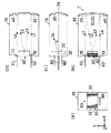
図1は本発明の一実施形態に係る光分波合波器1の斜視図を示しており、図2(A)はこの光分波合波器1の正面図、図2(B)は右側面図、図2(C)は平面図、図2(D)は左側面図(但し、右側面図とは上下が逆)である。本光分波合波器1は、内部空間11及びこの内部空間11と繋がる光入射口12及び光出射口13を有して構成されるケース10と、このケース10の内部空間11内に設けられた凹面反射面からなるコリメータ20と、ケース10に固定され、複数の直線状の回折溝31が等間隔に並べられてなる平面形の反射回折面32を有するグレーティング30と、ケース10の内部空間11内に設けられた凹面反射面からなるイメージングミラー40と、ケース10の光入射口12に接続された入射用光伝送路としての1本の入射用光ファイバ50と、ケース10の光出射口13に接続された出射用光伝送路としての複数の出射用光ファイバ60とを備えて構成される。以下、説明の便宜上、図2(A)における紙面の左右方向をケース10の左右(幅)方向、図2(B)における紙面の上下方向をケース10の上下方向、図2(B)における紙面の左右方向をケース10の左右方向(紙面の左側が前方、右側が後方)として説明する。また、ケース10の左右方向にX軸を、ケース10の上下方向にY軸を、またケース10の前後方向にZ軸を当てることにする。
【0017】
図1及び図2に示すように、コリメータ20とイメージングミラー40とはケース10の後部に上下に並んで設けられており(コリメータ20が上方、イメージングミラー40が下方)、グレーティング30の回折溝31はこのコリメータ20とイメージングミラー40とが並ぶ方向、すなわち上下方向に延びて設けられている。また、ケース10の内部空間11は光透過性のよい透明な固体媒質(例えば石英ガラス)Tmにより満たされた状態となっている。
【0018】
ケース10の前方中央部にはZ軸と垂直に位置する壁部14が設けられており、この壁部14の前方下方には、壁部14に対して垂直(すなわちXZ面に平行)に延びたグレーティング載置部15が設けられている。グレーティング30はこのグレーティング載置部15に回折溝31が上下方向に延びる姿勢で載置されており、その反射回折面32は空気を挟んで壁部14に(すなわちケース10の内部空間11に)対向している。ここで、グレーティング30は、その反射回折面32が壁部14と平行になるように設置されるのではなく、図2(C)に示すように、反射回折面32の法線GVがZ軸(図2(C)では軸ZXで示す)に対して或る程度の角度φだけ傾いた姿勢になるように設置される。
【0019】
壁部14には、グレーティング30の反射回折面32を壁部14に投影したときに形成される反射回折面32の投影像とほぼ同じ大きさの開口16が設けられている。
【0020】
光入射口12と光出射口13とは、グレーティング30の回折溝31の延びる方向(ここでは上下方向)にグレーティング30を挟んで、しかもグレーティング30からの距離がほぼ等距離になるように設けられている。光入射口12はグレーティング30の上方であって、コリメータ20とZ軸方向に沿って対向する位置に、また光出射口13はグレーティング30の下方であって、イメージングミラー40とZ軸方向に沿って対向する位置に設けられている。
【0021】
光入射口12には1本の入射用光ファイバ50が取り付けられており、光出射口13には入射用光ファイバ50を介してケース10の内部空間11内(固体媒質Tm内)に入射される波長分割多重光に含まれる波長数、言い換えると、本分波合波器1により分波しようとする波長数分の本数の出射用光ファイバ60がケース10の幅方向(X軸方向)に整列して取り付けられている。
【0022】
ここで、図3(A)に示すように、入射用光ファイバ50の端面はケース10の光入射口12から差し込まれた状態で内部空間11内の固体媒質Tmの表面に接合されるが、その接合面は、入射用光ファイバ50の中心軸線CX1の延びる方向(ここではZ軸方向)に垂直な面に対して所定の角度δ1(例えばδ1=8°)だけ傾斜していることが多い。これは、ファイバ切断面での反射光の戻りを防止するためである。したがって、入射用光ファイバ50からの射出光束は屈折作用を受けて偏向するが、これを相殺するだけの傾きを、固体媒質Tmの入射部に持たせてある。
【0023】
また同様に、図3(B)に示すように、各出射用光ファイバ60の端面はケース10の光出射口13から差し込まれた状態で内部空間11内の固体媒質Tmの表面に接合されるが、その接合面は、出射用光ファイバ60の中心軸線CX2の延びる方向(ここではZ軸方向)に垂直な面に対して所定の角度δ2(例えばδ2=8°)だけ傾斜していることが多い。これに応じて固体媒質Tmの射出部も入射部同様傾けている。
【0024】
入射用光ファイバ50及び出射用光ファイバ60は、それぞれケース10の光入射口12或いは光出射口13に取り付けた、反射損失の少ない材料からなる接着剤BDにより固着されている。ここで、入射用光ファイバ50と固体媒質Tmとの間の接合面、及び出射用光ファイバ60と固体媒質Tmとの間の接合面に屈折率マッチング用のゲル剤を充填させておいてもよい。また、このように屈折率マッチング用のゲル剤が充填される場合には、出射用光ファイバ60をケース10の光出射口13に完全に固定することなく、光出射口13に差し込んだ状態の出射用光ファイバ60の中心軸線CX2方向に微小量だけ移動自在としておくことが好ましい。このようにすることにより、波長ごとに分波された各光が対応する出射用光ファイバ60に入射する際のピント合わせを精度良く行うことができるようになる。
【0025】
このような構成の光分波合波器1において、入射用光ファイバ50より光が入射された場合における光の光路について、図1及び図2に図4を加えて説明する。ここで、図4は本光分波合波器1におけるケース10内の構成品を模式的に示すとともに光の進行状況を(A),(B),(C),(D)の順に示したものであり、図の左側の列はケース10内部の右側面図を示し、図の右側の列はケース10内部の平面図(但し、光の光路を示し易くするため、構成品の一部を適宜省略している)を示している。入射用光ファイバ50を介してケース10の内部空間11内に入った波長分割多重光は、ケース10の内部空間11を占める固体媒質Tm内を後方に進んでコリメータ20に入射する(図4(A)参照。この光をL1とする。図1、図2では主光線の光軸で示す)。この光L1は光入射口12を頂点とする円錐状の光束であるが、コリメータ20に反射されて平行光となり、固体媒質Tm内を前下方に進んで壁部14の開口16を通り、更に空気層を透過してグレーティング30の反射回折面32に至る(図4(B)参照この光をL2とする。図1、図2においては主光線の光軸で示す)。
【0026】
グレーティング30の反射回折面32に至った光はそこで反射回折されて波長の異なる複数の光に分光(分波)され、空気層及び開口16を通ってケース10の内部空間11内に入り、固体媒質Tm内を後下方に進んでイメージングミラー40に入射する(図4(C)参照。この光をL3とする。図1、図2においては主光線の光軸で示す)。ここで、グレーティング30に入射する光L2は平行光であるが、グレーティング30の反射回折面32は平面形で直線状の回折溝31を有するタイプであるので、その反射回折光L3もおおむね平行光のままとなる。なお、この反射回折光L3は入射光L1に含まれる波長ごとに分離して存在する。
【0027】
グレーティング30において反射した波長ごとの光は上述のように各々平行光であるが、イメージングミラー40において反射されて円錐状の光束となり、グレーティング30において分波された波長数を備えるスペクトラルイメージを形成して固体媒質Tm内を前方に進み、それぞれに対応する各出射用光ファイバ60の端面に至る(図4(D)参照この光をL4とする。図1、図2においては主光線の光軸で示す)。このように、本光分波合波器1においては、入射用光ファイバ50より入射された波長分割多重光は、波長ごとに分波された状態で出射用光ファイバ60より出射される。
【0028】
上記のように、本実施形態に係る光分波合波器1では、グレーティング30の反射回折面32は空気中に晒された回折面で光の回折を行う表面回折形であるが、反射回折面がこのような表面回折形であるか、後述する裏面反射形であるかを問わず、一般に反射回折面を有するグレーティングでは、光が反射回折される際に図5に示すようなアナモルフォシスが発生する。すなわち、図5(A)に示すように、グレーティングGへ入射するビームW1のビーム幅とグレーティングGで反射回折作用を受けた後のビームW2ビーム幅とが大きく異なってしまう。例えば、グレーティングGへ入射する光の断面形状(光軸に垂直な断面形状)が円形であった場合には、図示のように像面においては楕円形に変形することになり、図示はしないが、併せてビームの集光NA(開口数)も変形作用を受けることになる。したがって、グレーティングへの反射回折前後で光のアナモルフォシスが発生すると(アナモルフィック効果を受けると)、反射回折後の光を光ファイバへ入射させた際に大きな結合損失が発生してしまうことになる。
【0029】
これに対し、図5(B)に示すように、グレーティングGへ入射するビームW1のビーム幅とグレーティングGでの反射回折作用を受けた後のビームW2のビーム幅とに大きな差異が発生しなければ、上記のようなアナモルフォシスの発生を小さく抑えることができる(このとき、グレーティングGへ入射する光の断面帰依状が円形であった場合には、像面においてもほぼ円形となる)。すなわち、グレーティングは反射回折前後において光を等倍結合する構成であることが好ましい。このようにすれば、光分波合波器に光を入射させる側の光ファイバと光分波合波器より光を出射させる側の光ファイバとを同じもの(同じ材質、同じ径)にしたときには、原理的に高い結合効率が得られることになる。
【0030】
このような考え方から、本光分波合波器1においては、光入射口12と光出射口13とがグレーティング30の回折溝31の延びる方向に、グレーティング30を挟むように配設されている。このような構成によれば、グレーティング30へ入射する光束とグレーティング30において反射回折した光束とがなす角度(但し、反射回折後の光が分散する方向についての角度)を極めて小さくすることができ、その結果、反射回折前後におけるの光の断面形状の変形は小さくなり、グレーティング30において発生するアナモルフィック効果を大幅に低減させることができる
【0031】
このため本光分波合波器1では、入射した波長分割多重光とグレーティング30における反射回折後の波長ごとに分波された各光との間のNAの差は極めて小さいものとなり(すなわちNAが高レベルに保存され)、小型でありながら低損失な性能が得られる。また、このような性能を備えることにより、本分波合波器1をWDM光通信に適用した場合、従来技術のうち誘電体多層膜ダイクロイックミラー方式やファイバーブラッググレーティング方式が4波程度の分波・合波が普通なのに対し、小型ながらより多くの波長チャネルを同時に扱うことが可能となる。更に、アナモルフォシスの発生を抑えた結果、イメージ(像)の変形が小さくなり、例えば等倍の像に結像させた場合、入射側光ファイバ端のモードフィールド像がイメージとしてよく再現され、同時に光ファイバのNAも忠実に再現されることになる。更に本分波合波器1によれば、後述する実施例において示すように、像点における収差が良好に補正される。
【0032】
また、これらの特徴は、従来のグレーティング分光器方式のものよりも光ファイバへの光エネルギーの結合効率を高める効果があり、使用波長域にグレーティングのブレーズ波長域が合致した場合、従来のいずれの方式にもない、低い内部損失での分波・合波を実現できる可能性を秘めている。また、非常に小型化されるという特徴は、省スペースが強く要求される光通信アクセス系の光学部品として適している。更に、本分波合波器1は、光ファイバアレイ以外は一体構造となっているので、機械的安定性が抜群に良い分波・合波が実現できる点も光通信アクセス系の光学部品として適している。
【0033】
また、本光分波合波器1で、上述したように、ケース10の内部空間11内は光透過性のよい固体媒質Tmにより満たされている。なお、ここでは内部空間11内に満たされる透明媒質は固体であるが、これは光透過性のよい液体(ゲル状の物質を含む)であってもよい。或いは、ケース10の内部空間11は単なる空洞であってもよい。但し、この場合には内部は真空状態であることがより好ましい。また、このようにケース10の内部空間11が空洞或いは液体で満たされるときには、光入射用光ファイバ50の端面及び光出射用光ファイバ60の端面は、内部空間11内或いは液体内に晒された状態となる。
【0034】
ここで、本光分波合波器1のように、内部空間11を透明な固体媒質Tmが満たす構成であるときには、予め所定の形状にした固体媒質Tmにコリメータ20及びイメージングミラー40を取り付けてこれらを一体構造(モノリシックな構成)とした上で固体媒質Tmをケース10により覆い、これに入射用光ファイバ50及び出射用光ファイバ60を取り付けるという手順で本光分波合波器1を製造することができるので、製造工程が大変簡易になる。
【0035】
また、本光分波合波器1では、上述したように、入射用光ファイバ50と固体媒質Tmとの接続面、及び出射用光ファイバ60と固体媒質Tmとの接続面にはともに傾斜が付けられていたが、これら双方の接続面は互いに平行であることが好ましい。例えば、アライメントエラーにより入射用光ファイバ50の固体媒質Tm表面上への取り付け位置が本来の位置よりも上方にずれてしまった場合には、入射光束L1の主光線が上方にずれるとともに、出射光束L4の主光線も同じ量だけ下方にずれるのであるが、ここで、図3に示すような方向の傾斜が上記両接続面に平行に設けられているとすると、入射用光ファイバ50の取り付け位置が上方にずれたときには上記傾斜により光の入射口12は入射用光ファイバ50側(図3では紙面の左方)にもずれており、光の入射点はコリメータ20から僅かに遠ざかることになる。一方、これにより像点はイメージングミラー40に近づくことになるが、上記のようにこの像点は光の入射点が上方にずれた分だけ下方にずれるので、ちょうど出射用光ファイバ60と固体媒質Tmとの接続面上に位置して結像することになる。このように、入射用光ファイバ50と固体媒質Tmとの接続面、及び出射用光ファイバ60と固体媒質Tmとの接続面が互いに平行であれば、アライメントエラーにより生ずる結像点の位置ずれは自動的に修正される。
【0036】
また、本光分波合波器1においては、イメージングミラー40の焦点がグレーティング30の反射回折面32上(若しくはその近傍位置)に位置していることが好ましい。イメージングミラー40がこのように配置されているのならば、グレーティング30の反射回折面32において反射回折されて波長ごとに分光(分波)された各光束は、グレーティング30を上方より見た図6より分かるように、イメージングミラー40において反射した後、各波長ごとの光の主光線は互いに平行となる(すなわちテレセントリックな結像態様となる)。
【0037】
ここで、ケース10の光出射口13繋がる複数の出射用光ファイバ60が平行に配列されており、かつ、上記した各出射用光ファイバ60の端面カットの角度が全て同じで互いに平行になるように処理されているのであれば、各波長ごとの光の結像光線(の主光線)はほぼ等しい角度で、対応する出射用光ファイバ60のコア61に入射することになる。したがって、イメージングミラー40において反射した波長ごとの光L4の出射用光ファイバ60への入射角度を最適値に調節すれば、固体媒質Tmと出射用光ファイバ60との間の結合損失を低減させて、本光分波合波器1全体としての損失をより一層低減させることが可能となる。
【0038】
また、上記実施形態において示したグレーティング30は、空気中に晒された反射回折面32において反射回折を行う表面反射形のグレーティングであったが、このような表面反射形のグレーティングを用いれば、ケース10の内部空間11内を占める媒質(固体とは限らない)の屈折率の温度変化が問題となる場合において有効となる。すなわち、一般にガラスなどの固体、液体からなる媒質は屈折率の温度変化が気体に比べて大きく、屈折率が変化すると上記媒質内を伝播中の光の波長が変化してしまう。その結果、グレーティングによる回折角度に変動が生じ、像点位置のドリフトが生じる虞がある。ここで、上記実施形態において示したように、グレーティングの反射回折面を空気中に晒し、空気層を介して光の反射回折を行うようにすることにより、温度変化による像点ドリフトを大幅に軽減させることができる。
【0039】
また、コリメータ20及びイメージングミラー40は上述したように、ともに凹面反射面であるが、本光分波合波器1ではこれを特に回転放物面形状とすることにより、波長ごとに分波した各光L4を対応する出射用光ファイバ60へ結合させるときに生じる結合損失を低減させて本分波合波器1全体としての損失を低下させることができる。具体的には、図7に示すように、コリメータ20及びイメージングミラー40がそれぞれ同一の回転放物面PS上の異なる一部分となるようにするとともに、回転放物面PSの生成回転軸PXが入射用光ファイバ50を介してケース10の内部空間11内(固体媒質Tm内)に入射した光L1の主光線に対して平行となり、かつ、回転放物面PSの焦点PFがグレーティング30の反射回折面32上(若しくはその近傍位置)に位置するようにコリメータ20及びイメージングミラー40を配置する。
【0040】
コリメータ20及びイメージングミラー40が上記のように配置された場合、入射用光ファイバ50を介してケース10の内部空間11内(固体媒質Tm内)に入射した光L1がコリメータ20において反射した光L2の主光線はグレーティング30の反射回折面32上に至るが、この光L2の主光線の光軸が反射回折面32と交わる点は、コリメータ20及びイメージングミラー40の表面形状を含んでなる回転放物面PSの生成回転軸PX上に位置し、しかも、その回転放物面PSの焦点PFに一致(或いはほぼ一致)する。このとき、グレーティング30の反射回折面32において反射回折した光L3は回転放物面PSの焦点PFより発する光となるため、その回転放物面PSの一部であるイメージングミラー40において反射した光L4の主光線は回転放物面PSの生成回転軸PX、及び光L1の主光線の光軸と平行になる(テレセントリックな結像態様となる)。
【0041】
ここで、上述したように、ケース10の光出射口13に繋がる複数の出射用光ファイバ60の列が平行に配列されており、かつ、上記した各出射用光ファイバ60の端面カットの角度が全て同じで互いに平行になるように処理されているのであれば、各波長ごとの光の結像光線(の主光線)はほぼ等しい角度で、対応する出射用光ファイバ60のコア61に入射することになるため、イメージングミラー40において反射した波長ごとの光L4の出射用光ファイバ60への入射角度を最適値に調節すれば、固体媒質Tmと出射用光ファイバ60との間の結合損失を低減させて、本光分波合波器1全体としての損失をより一層低減させることが可能となる。
【0042】
ここでもし、グレーティング30をただの平面ミラーに置き換えて、その反射面をコリメータ20及びイメージングミラー40の表面形状を含んでなる回転放物面PSの生成回転軸PXに垂直に設置するならば、入射用光ファイバ50を介してケース10の内部空間11内(固体媒質Tm内)に入射し、コリメータ20、平面ミラー、イメージングミラー40を経て、出射用光ファイバ60の端面にできる入射用光ファイバ50の端面像は、おおよそアプラナティックな結像をすることになり、幾何光学的収差が非常に小さくなる。本光分波合波器1のようにグレーティング30をグレーティングとして作用させてもその傾向は残るので、やはり幾何光学的収差は大変小さくなる。
【0043】
また、上記のようにコリメータ20及びイメージングミラー40の表面形状が回転放物面となるようにする代わりに、コリメータ20及びイメージングミラー40の表面形状がをトーリック面となるようにすることによっても、波長ごとに分波した各光L4を対応する出射用光ファイバ60へ結合させるときに生じる結合損失を低減させて本分波合波器1全体としての損失を低下させることができる。
【0044】
具体的な説明に入る前に、先ずトーリック面について説明する。トーリック面には図8に示すように2つのタイプがあり、そのトーリック面の生成回転軸AXを通る平面を経面M、生成軸AXに垂直な平面のうちトーリック面との交円が大円となる平面を赤道面Eとした場合、赤道面Eによりトーリック面自身を切断したときに交円が1つ得られるタイプのもの(第1のタイプのトーリック面とする)と、赤道面Eによりトーリック面自身を切断したときに交円が2つ得られるタイプのもの(第2のタイプのトーリック面とする)とが存在する。図8(A)は前者の例を示しており、図8(B)は後者の例を示している。これら両タイプのトーリック面とも大きさの異なる2つの曲率半径を有しているが、このうち大きい方の曲率半径をタンジェンシャル(メリジオナル)方向の曲率半径Rt、小さい方の曲率半径がサジタル方向の曲率半径Rsとする。
【0045】
ここで、コリメータ20及びイメージングミラー40の表面形状を含むトーリック面として上記第1のタイプを採用する場合には、図9に示すように、コリメータ20及びイメージングミラー40がそれぞれ同一のトーリック面TS上の異なる一部分となるようにしたうえで、これらコリメータ20及びイメージングミラー40を、▲1▼そのトーリック面TSの経面Mのうち選択された一つ(経面M1とする)が入射用光ファイバ50を介してケース10の内部空間11内(固体媒質Tm内)に入射する光L1の主光線の光軸に対して平行になるとともに、▲2▼その選択された経面M1内方向の焦点RMFが反射回折面32上(若しくはその近傍位置)に位置し、かつ、▲3▼上記選択された経面M1が、上記光L1の主光線を含んでグレーティング30の回折溝31と平行な方向に延びる平面BS1と0°ないし45°の範囲で交わる(図9中に示す角度Ψ1が0≦Ψ1≦45°の範囲となる)位置に設ける。
【0046】
一方、コリメータ20及びイメージングミラー40を含むトーリック面として上記第2のタイプを採用する場合には、図10に示すように、コリメータ20及びイメージングミラー40がそれぞれ同一のトーリック面TS上の異なる一部分となるようにしたうえで、これらコリメータ20及びイメージングミラー40を、▲1▼そのトーリック面TSの赤道面Eのうち選択された一つ(赤道面E1とする)が上記光L1の主光線の光軸に対して平行になるとともに、▲2▼その選択された赤道面E1内方向の焦点REFが反射回折面32上(若しくはその近傍位置)に位置し、かつ、▲3▼上記選択された赤道面E1が、上記光L1を含んでグレーティング30の回折溝31と平行な方向に延びる平面BS2と0°ないし45°の範囲で交わる(図10中に示す角度Ψ2が0≦Ψ2≦45°の範囲となる)位置に設ける。
【0047】
コリメータ20及びイメージングミラー40が上記のように配置された場合、トーリック面TSが第1のタイプであるときには、入射用光ファイバ50を介してケース10の内部空間11内(固体媒質Tm内)に入射した光L1がコリメータ20において反射した光L2の主光線はグレーティング30の反射回折面32上に至るが、この光L2の主光線の光軸が反射回折面32と交わる点は、コリメータ20及びイメージングミラー40の表面形状を含んでなるトーリック面TSの生成回転軸AX上に位置し、しかも、そのトーリック面TSの選択された経面M1内方向の焦点RMFに一致(或いはほぼ一致)する。このとき、グレーティング30の反射回折面32において反射回折した光L3はトーリック面TSの上記焦点RMFより発する光となるため、そのトーリック面TSの一部であるイメージングミラー40において反射した光L4の主光線はトーリック面TSの生成回転軸AX、及び光L1の主光線の光軸と平行になる(テレセントリックな結像態様となる)。
【0048】
また、トーリック面TSが第2のタイプであるときには、入射用光ファイバ50を介してケース10の内部空間11内(固体媒質Tm内)に入射した光L1がコリメータ20において反射した光L2の主光線はグレーティング30の反射回折面32上に至るが、この光L2の主光線の光軸が反射回折面32と交わる点は、コリメータ20及びイメージングミラー40の表面形状を含んでなるトーリック面TSの生成回転軸AX上に位置し、しかも、そのトーリック面TSの選択された赤道面E1内方向の焦点REFに一致(或いはほぼ一致)する。このとき、グレーティング30の反射回折面32において反射回折した光L3はトーリック面TSの上記焦点REFより発する光となるため、そのトーリック面TSの一部であるイメージングミラー40において反射した光L4の主光線はトーリック面TSが第1のタイプである場合と同様、トーリック面TSの生成回転軸AX、及び光L1の主光線の光軸と平行になる(テレセントリックな結像態様となる)。
【0049】
ここで、上述したコリメータ20及びイメージングミラー40の表面形状を回転放物面とする場合と同様、ケース10の光出射口13に繋がる複数の出射用光ファイバ60の列が平行に配列されており、かつ、上記した各出射用光ファイバ60の端面カットの角度が全て同じで互いに平行になるように処理されているのであれば、各波長ごとの光の結像光線(の主光線)はほぼ等しい角度で、それぞれに対応する出射用光ファイバ60のコア61に入射することになるため、イメージングミラー40において反射した波長ごとの光L4の出射用光ファイバ60への入射角度を最適値に調節すれば、固体媒質Tmと出射用光ファイバ60との間の結合損失を低減させて、本光分波合波器1全体としての損失をより一層低減させることが可能となる。
【0050】
ここで、トーリック面が第1のタイプであるか第2のタイプであるかに拘わらず、光L1の主光線の光軸がコリメータ20上の反射点法線となす角をθ1とすると、光L2の主光線の光軸が上記コリメータ20上の反射点法線となす角もθ1となり、光L3の主光線の光軸がイメージングミラー40上の反射点法線となすをθ2とすると、光L4の主光線の光軸が上記イメージングミラー40上の反射点法線となす角もθ2となる。グレーティング30の反射回折面32に入射した光の入射角度と、反射回折面32において反射した光の出射角度はほぼ等しいことから、上記θ1とθ2とはほぼ等しくなり(θ1≒θ2)、その角度をθとおくと、光L1の主光線の光軸と光L2の主光線の光軸とがなす角度は2θとなり、光L3の主光線の光軸と光L4の主光線の光軸とがなす角度も2θとなる(図9及び図10参照)。
【0051】
また、上記のようにコリメータ20及びイメージングミラー40をトーリック面とする場合、更に下に示す条件を満たすようにすることにより、コリメータ20及びイメージングミラー40において光が反射することにより生ずる幾何光学的収差を容易に抑えることが可能である。その具体的な説明に入る前に、先ず、図11を用いて凹トーリック反射面のパワーについて説明する。
【0052】
図11は、凹トーリック反射面MSの反射点Rpでの法線RpVに対して角度θで平行光束が入射して反射する様子を示している。ここで、光束Ltは上記平行光束の凹トーリック反射面MSのタンジェンシャル方向(メリジオナル)入射成分、光速Lsは上記平行光束の凹トーリック反射面MSのサジタル方向入射成分である。凹トーリック反射面MSに、反射点Rpでの法線RpVに対して角度θで入射する光束について、タンジェンシャル方向(図中にTで示す方向)の焦点距離とサジタル方向での焦点距離を一致させるためには、その凹面反射面MSの反射点Rpでの2つの曲率半径Rt,Rs(図9及び図10も参照)について、焦点距離をfとしたときに(この焦点距離fは、図11における反射点Rpと光の集光点BFとの間の距離となる)、下式(1),(2)が満たされるようにすればよい。
【0053】
【数1】
タンジェンシャル方向: Rt=2・f/cosθ … (1)
サジタル方向: Rs=2・f・cosθ … (2)
【0054】
上記両式(1),(2)より、下式(3)が導かれる。
【0055】
【数2】
Rs/Rt=cos2θ … (3)
【0056】
図9及び図10において示したθの値を上式(3)に当てはめてこれが成り立つとき、コリメータ20及びイメージングミラー40において反射する光の非点収差の発生が抑えられることになるので、非点収差による像の伸び変形が発生しない。したがって、受光側でファイバ結合効率を高く維持でき、損失をより小さく抑えることが可能となる。
【0057】
これまで本発明の好ましい実施形態について説明してきたが、本発明の範囲は上述の実施形態に示したものに限定されない。例えば、上述の実施形態では、コリメータ20とイメージングミラー40とを別部材からなっていたが、これらは一体に形成されるものであってもよい。特に、コリメータ20及びイメージングミラー40の表面形状を回転放物面、或いはトーリック面とする場合には、製作及び構成が非常に簡単になる。
【0058】
また、上述の実施形態においては、グレーティング30の反射回折面32は空気を隔ててケース10の内部空間11(固体媒質Tm)と対向するようになっていたが、反射回折面32は必ずしも空気を隔ててケース10の内部空間と対向するようになっている必要はない。例えば、図12及び図13に示すように、グレーティング30’が複数の直線状の回折溝31’が等間隔に並べられてなる反射回折面32’を有しており、この反射回折面32’が、グレーティング30’を構成する媒質内に形成されているところの、裏面反射形であってもよい。このとき、コリメータ20において反射された光L2は、固体媒質Tmよりグレーティング30を構成する材質(例えば石英ガラス)を透過して反射回折面32’に至り、反射回折後の光は再びグレーティング30を構成する材質を透過して固体媒質Tm内に入り、イメージングミラー40に至る光路をとることになる(このときのグレーティング30’は裏面反射形のグレーティングとなる)。なお、図12はこのような変形例に係る光分波合波器1’の斜視図であり、図13(A)はこの光分波合波器1’の正面図、(B)は右側面図、(C)は平面図、(D)は左側面図(但し、右側面図とは上下が逆)である。また、これら両図では、上述の実施形態と同じ構成のものには同じ符号を付している。なお、表面反射形であってもこれをケース10の内部空間11内(或いはこの内部空間11を満たす固体媒質Tm内)に位置させることもできる。
【0059】
また、本発明に係る光分波合波器を光合波器として用いた場合には、光の入出力方向が全く逆になる。すなわち、上記各出射用光ファイバ60よりケース10の内部空間11内(固体媒質Tm内)に入射された、異なる波長を有する複数の光は、イメージングミラー40において反射された後、グレーティング30の反射回折面32に至って反射回折され、一つの光に合波された状態となってコリメータ20に至り、ここで反射されて入射用光ファイバ50に入射されることになる。また、本光分波合波器は、上述のように、波長分割多重光の分波及び波長分割多重光への合波に用いることができるが、その用途は必ずしもこれら光の分波・合波に限定されるものではない。
【0060】
【実施例】
以下、本発明に係る分波合波器の具体的な実施例について示す。
【0061】
(第1実施例)
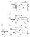
図14は本発明の第1実施例に係る光分波合波器を示すものであり、(A)は分波合波器の正面図(但し、入射光用光ファイバ50と出射用光ファイバ60のみを示す)、(B)は右側面図、(C)は平面図である。この第1実施例に係る光分波合波器では、コリメータ20及びイメージングミラー40を回転放物面から形成しており、ケース10の内部空間11内は後記する屈折率特性を有する固体媒質Tmで満たした。グレーティング30は裏面反射形であり(上述の実施形態の変形例に係る光分波合波器1’に相当)、反射回折面32’と対向する側の面はケース10の壁部14に設けた貫通穴(図示せず)を介して固体媒質Tmと接合させた。また、グレーティング30上の光の反射点を原点として、XYZ座標系を図14のように設定した。主要諸元及び入射点、像点の座標データを下の表1に示す。
【0062】
【表1】
主要部寸法: A=30.5mm, B=30mm
固体媒質の波長に対する屈折率特性:図15の表に示す
分波波長: 1371mm,1391mm,1411mm,1431mm,1461mm,1491mm,1511mm,1531mm,1551mm,1571mm,1591mm,1611mm,1631mm,1651mm,1671mm,1691mmの16波
グレーティング
格子定数:1/400mm
回折字数:1次
溝方向:Y軸に平行
反射回折面の法線GVがZ軸となす角度φ: 11.907°
入射点の座標: X=−0.5mm, Y=5.5mm
像点の座標: 図16の表に示す
【0063】
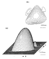
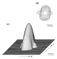
像点での結像性能の一例を図17に示す。この結像性能を示す図は、上記16の分波波長より選択した波長1571mmの光の像点における強度分布を立体表示(図17(A))とコンター表示(図17(B))にて示したものである(単位デシベル)。図17(B)においてコンター表示は、頂点を0dBとし、−30dBまで3dB刻みで示した。なお、本実施例では、光の入射面及び像面は、回転放物面の生成回転軸に垂直な平面であるとした。
【0064】
(第2実施例)
図18は本発明の第2実施例に係る光分波合波器を示すものであり、(A)は分波合波器の正面図(但し、入射光用光ファイバ50と出射用光ファイバ60のみを示す)、(B)は右側面図、(C)は平面図、(D)は左側面図(但し、右側面図とは上下が逆)である。この第2実施例に係る光分波合波器では、コリメータ20及びイメージングミラー40を回転放物面から形成しており、ケース10の内部空間11内は上記第1実施例と同じ屈折率特性を有する固体媒質Tmで満たした。グレーティング30は表面反射形であり(上述の実施形態に係る光分波合波器1に相当)、反射回折面32は空気を隔てて固体媒質Tmと対向するように位置させた。また、グレーティング30上の光の反射点を原点として、XYZ座標系を図18のように設定した。主要諸元及び入射点、像点の座標データを下の表2に示す。
【0065】
【表2】
主要部寸法: A=30.51mm, B=27.5mm, C=1.7mm
固体媒質の波長に対する屈折率特性:図15の表と同じ
分波波長: 第1実施例と同じ16波
グレーティング
格子定数:1/400mm
回折字数:1次
溝方向:Y軸に平行
反射回折面の法線GYがZ軸となす角度φ: 17.5°
入射点の座標: X=−0.5mm, Y=5.5mm
像点の座標: 図19の表に示す
【0066】
像点での結像性能の一例を図20に示す。この結像性能を示す図は、上記16の分波波長より選択した波長1571mmの光の像点における強度分布を立体表示(図20(A))とコンター表示(図20(B))にて示したものである(単位デシベル)。図20(B)においてコンター表示は、頂点を0dBとし、−30dBまで3dB刻みで示した。なお、本実施例では、光の入射面及び像面は、回転放物面の生成回転軸に垂直な平面であるとした。
【0067】
(第3実施例)
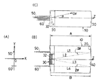
図21は本発明の第3実施例に係る光分波合波器を示すものであり、(A)は分波合波器の正面図(但し、入射光用光ファイバ50と出射用光ファイバ60のみを示す)、(B)は右側面図、(C)は平面図である。この第3実施例に係る光分波合波器では、コリメータ20及びイメージングミラー40を前述した第2のタイプのトーリック面から形成しており、ケース10の内部空間11内は上記第1実施例と同じ屈折率特性を有する固体媒質Tmで満たした。グレーティング30は裏面反射形であり(上述の実施形態の変形例に係る光分波合波器1’に相当)、反射回折面32’と対向する側の面はケース10の壁部14に設けた貫通穴(図示せず)を介して固体媒質Tmと接合させた。また、グレーティング30上の光の反射点を原点として、XYZ座標系を図21のように設定した。主要諸元及び入射点、像点の座標データ等を下の表3に示す。
【0068】
【表3】
主要部寸法: A=30.31mm, B=30mm
固体媒質の波長に対する屈折率特性:図15の表と同じ
分波波長: 第1実施例と同じ16波
トーリック面
曲率半径:Rt=60.404mm,Rs=60mm(Rs/Rt=0.993)
グレーティング
格子定数:1/400mm
回折字数:1次
溝方向:Y軸に平行
反射回折面の法線GVがZ軸となす角度φ:12°
入射点の座標: X=−0.5mm, Y=5.5mm
像点の座標: 図22の表に示す
図10中に示す角度Ψ2: 90°
図21中に示す角度θ: 5.2°(cos2θ=0.992≒Rs/Rt)
【0069】
像点での結像性能の一例を図23に示す。この結像性能を示す図は、上記16の分波波長より選択した波長1571mmの光の像点における強度分布を立体表示(図23(A))とコンター表示(図23(B))にて示したものである(単位デシベル)。図23(B)においてコンター表示は、頂点を0dBとし、−30dBまで3dB刻みで示した。なお、本実施例では、光の入射面及び像面は、回転放物面の生成回転軸に垂直な平面であるとした。
【0070】
上記第1〜第3実施例についての結果を見ると、分波後の波長は、中央部の光強度が周辺部の光強度よりも際立って高い、ガウスビーム形の強度分布となっている。また、収差も良好に補正されている。これらのことから、本発明に係る光分波合波器は、入射から出射までNAが高レベルに保存されて損失が小さく抑えられ、多波長(これら実施例では16波長)を扱いながらも良好な結像性能を有していることが分かる。
【0071】
【発明の効果】
以上説明したように、本発明に係る光分波合波器では、光入射口と光出射口とが、グレーティングにおける回折溝の延びる方向に、グレーティングを挟んで設けられているため、グレーティングへの入射光束とグレーティングからの反射回折光束とがなす、反射回折後の光が分散する方向についての角度を極めて小さくすることができ、反射回折の前後における光のアナモルフィック効果を大幅に低減させることができる。このため、入射した波長分割多重光とグレーティングにおける反射回折後の波長ごとに分波された各光との間のNAの差は極めて小さいものとなり(すなわちNAが高レベルに保存され)、小型でありながら低損失な性能が得られる。また、このような性能を備えることにより、本光分波合波器をWDM光通信に適用した場合、従来技術のうち誘電体多層膜ダイクロイックミラー方式やファイバーブラッググレーティング方式が4波程度の分波・合波が普通なのに対し、小型ながらより多くの波長チャネルを同時に扱うことが可能となる。
【図面の簡単な説明】
【図1】本発明の一実施形態に係る光分波合波器の斜視図である。
【図2】光分波合成器を示す図であり、(A)は正面図、(B)は右側面図、(C)は平面図、(D)は左側面図である。
【図3】(A)は入射用光ファイバと固体媒質との接合部を示すケースの部分拡大側面図であり、(B)は各出射用光ファイバと固体媒質との接合部を示すケースの部分拡大側面図である。
【図4】光分波合波器1におけるケース内の構成品を模式的に示すとともに光の進行状況を(A),(B),(C),(D)の順に示したものであり、左側の列はケース内部の右側面図を示し、右側の列はケース内部の平面図を示している。
【図5】グレーティングにおいて光が反射回折される際に生じるアナモルフォシスの発生を説明する図であり、(A)はグレーティングへ入射するビームのビーム幅とグレーティングで回折作用を受けた後のビームのビーム幅とが大きく異なる場合の例、(B)は上記両ビーム幅に大きな差異が生じない場合の例である。
【図6】グレーティングの反射回折面において反射回折されて波長ごとに分光された各光束が互いに平行となる様子を示す、グレーティングを上方から見た図である。
【図7】コリメータ及びイメージングミラーがそれぞれ同一の回転放物上の異なる一部分となるようにした場合の光の光路を示すケース内部の簡略側面図である。
【図8】トーリック面の2つのタイプを示す図であり、(A)は赤道面によりトーリック面自身を切断したときに交円が1つ得られる第1のタイプのトーリック面を示し、(B)は赤道面によりトーリック面自身を切断したときに交円が2つ得られる第2のタイプのトーリック面を示している
【図9】第1のタイプのトーリック面を採用した場合のコリメータ及びイメージングミラーの配置を説明するための図である。
【図10】第2のタイプのトーリック面を採用した場合のコリメータ及びイメージングミラーの配置を説明するための図である。
【図11】凹トーリック反射面のパワーについて説明するための図である。
【図12】変形例に係る光分波合波器の斜視図である。
【図13】変形例に係る光分波合波器を示す図であり、(A)は正面図、(B)は右側面図、(C)は平面図、(D)は左側面図である。
【図14】本発明の第1実施例に係る光分波合波器を示す図であり、(A)は正面図、(B)は右側面図、(C)は平面図である。
【図15】第1実施例において用いられる固体媒質の波長に対する屈折率特性を示す図表である。
【図16】第1実施例において得られる像点の座標を示す図表である。
【図17】第1実施例において得られる像点での結像性能の一例を示す図であり、(A)は波長1571mmの光の像点における強度分布を立体表示したもの、(B)はこれをコンター表示したものである。
【図18】本発明の第2実施例に係る光分波合波器を示す図であり、(A)は正面図、(B)は右側面図、(C)は平面図、(D)は左側面図である。
【図19】第2実施例において得られる像点の座標を示す図表である。
【図20】第2実施例において得られる像点での結像性能の一例を示す図であり、(A)は波長1571mmの光の像点における強度分布を立体表示したもの、(B)はこれをコンター表示したものである。
【図21】本発明の第3実施例に係る光分波合波器を示す図であり、(A)は正面図、(B)は右側面図、(C)は平面図である。
【図22】第3実施例において得られる像点の座標を示す図表である。
【図23】第3実施例において得られる像点での結像性能の一例を示す図であり、(A)は波長1571mmの光の像点における強度分布を立体表示したもの、(B)はこれをコンター表示したものである。
【図24】従来の光分波合波器の第1例を示す図である。
【図25】従来の光分波合波器の第2例を示す図である。
【符号の説明】
1 光分波合波器
10 ケース
11 内部空間
12 光入射口
13 光出射口
15 グレーティング載置部
20 コリメータ
30 グレーティング
31 回折溝
32 反射回折面
40 イメージングミラー
50 入射用光ファイバ
60 出射用光ファイバ[0001]
TECHNICAL FIELD OF THE INVENTION
The present invention relates to an optical demultiplexer / demultiplexer that demultiplexes or multiplexes communication light in optical communication performed using wavelength division multiplexed light.
[0002]
[Prior art]
An optical demultiplexer / multiplexer in WDM (wavelength division multiplexing) optical communication known as a conventional technique uses, for example, a dielectric multilayer dichroic mirror, a fiber Bragg grating (FBG), a grating spectroscope, and an AWG (array waveguide grating). Have been put to practical use. Among them, those using a dielectric multilayer dichroic mirror and a fiber Bragg grating have about 4 channels, and those using AWG mainly have about tens of channels. A grating spectroscope-type optical demultiplexer / multiplexer can realize several channels to several tens of channels, but is suitable for WDM optical communication, which does not require as many channels as an AWG type optical demultiplexer / multiplexer. And some attempts have been made in the past.
[0003]
An optical demultiplexer / multiplexer for WDM optical communication is required to have, above all, a small size and low loss. As an example taking this point into consideration, for example, as shown in FIG. 24, an optical demultiplexer / multiplexer using a gradient
[0004]
[Problems to be solved by the invention]
The main factors that determine the throughput in the optical splitter / multiplexer of the grating spectroscope type are the diffraction efficiency of the grating, the anamorphic effect caused by the grating, and the magnitude of the geometrical optical aberration generated in the constituent optical system. Since the diffraction efficiency of the grating must be as high as possible, it is necessary to reduce the anamorphic effect caused by the grating and to realize a compact, low-loss optical demultiplexer / multiplexer. It is necessary to reduce the generated geometrical optical aberration.
[0005]
In the present invention, by reducing the anamorphic effect caused by the grating and reducing the geometrical optical aberration generated in the constituent optical system, an optical demultiplexing / multiplexing that can obtain a small-size but low-loss performance is achieved. The purpose is to provide a vessel.
[0006]
[Means for Solving the Problems]
An optical demultiplexer / multiplexer according to the present invention includes a case having an internal space, a light entrance and a light exit which are connected to the internal space, and an optical transmission for incidence connected to the light entrance of the case. Path, a plurality of outgoing light transmission paths connected to the light output port of the case, and a wavelength division multiplexed light that is provided in the inner space of the case and is incident on the inner space through the incident light transmission path. A first concave reflecting surface that reflects the light into parallel light, and a plurality of linear diffraction grooves fixed to the case and arranged to convert the wavelength division multiplexed light parallelized on the first concave reflecting surface into a plurality of linear diffraction grooves. A grating that splits the light into a plurality of lights having different wavelengths on a planar reflection / diffraction surface, and a second concave reflection that is provided in the internal space of the case and causes the light split by the grating to enter the light transmission path for emission. A light entrance and a light exit. , The extending direction of diffraction grooves on the grating, is provided across the grating.
[0007]
In the optical demultiplexer / multiplexer according to the present invention, the wavelength division multiplexed light that has entered the internal space of the case via the incident light transmission path is reflected by the first concave reflecting surface to become parallel light, and is converted into a parallel light by the grating. Incident. The light incident on the grating is split into a plurality of lights having different wavelengths, reflected on the second concave reflecting surface, and then emitted to the corresponding emission optical transmission lines. Here, the grating has a planar reflection diffraction surface in which a plurality of linear diffraction grooves are arranged at equal intervals, and splits the incident wavelength division multiplexed light into a plurality of lights having different wavelengths. However, since the light entrance and the light exit are provided with the grating interposed therebetween in the direction in which the diffraction groove in the grating extends, the light flux incident on the grating and the diffracted light flux reflected from the grating make a reflection. The angle in the direction in which the diffracted light is dispersed can be made extremely small, and the anamorphic effect of light before and after reflection diffraction can be greatly reduced.
[0008]
For this reason, in the optical demultiplexer / multiplexer according to the present invention, the difference in NA between the incident wavelength division multiplexed light and each light demultiplexed for each wavelength after reflection and diffraction in the grating is extremely small (that is, the difference in NA). NA is preserved at a high level), and a small size and low loss performance can be obtained. Also, by providing such a performance, when the present demultiplexer / demultiplexer is applied to WDM optical communication, the dielectric multilayer dichroic mirror method and the fiber Bragg grating method among the conventional techniques are capable of demultiplexing about four waves. While multiplexing is common, it is possible to handle more wavelength channels at the same time while being small.
[0009]
Here, in the optical demultiplexer / demultiplexer, the interior space of the case is filled with a transparent solid medium, and the end face of the light transmission path for incidence and the end face of the light transmission path for emission are respectively connected to the solid medium. Preferably, they are joined. In this way, the scattering loss caused by the progress of light can be reduced, and the loss of the entire optical demultiplexer / multiplexer can be further reduced. According to such a configuration, the first concave reflecting surface and the second concave reflecting surface are attached to a transparent solid medium having a predetermined shape in advance to form an integral structure (monolithic structure). The optical demultiplexer / multiplexer can be manufactured by covering the solid medium with a case, and attaching the incident light transmission path and the output light transmission path to the solid medium, thereby greatly simplifying the manufacturing process.
[0010]
In the optical demultiplexer / multiplexer, the reflection / diffraction surface faces the internal space of the case via the air, and the light reflected by the first concave mirror passes through the opening provided in the case and the air. It is preferable that the light incident on the reflection diffraction surface and reflected and diffracted by the reflection diffraction surface reaches the second concave mirror through the air and the opening. The reason is that air has a small change in refractive index with temperature as compared with a medium such as glass, so that the wavelength fluctuation of light is also small. Of course, a vacuum is even better. If the wavelength fluctuation of the light is large, the diffraction angle of the grating also fluctuates greatly, which causes a drift of the image forming position, which is not preferable.
[0011]
In the optical demultiplexer / multiplexer, it is preferable that the focal point of the second concave reflecting surface is located on or near the reflection diffraction surface of the grating. With such a configuration, each light flux reflected and diffracted on the reflection diffraction surface of the grating and separated for each wavelength is reflected on the second concave reflection surface, and the principal rays of light for each wavelength are parallel to each other. (A telecentric imaging mode), a plurality of output light transmission paths connected to the light output port of the case are arranged in parallel, and the angle of the end face cut of each output light transmission path is all If they are processed so as to be parallel to each other, (the chief ray of) the image-forming light beam of each wavelength enters the corresponding output light transmission path at substantially the same angle. Therefore, by adjusting the angle of incidence of the light for each wavelength reflected on the second concave reflecting surface to the emission optical transmission line to an optimum value, the coupling loss between the light and the emission optical transmission line can be reduced, and It is possible to further reduce the loss of the entire optical demultiplexer / multiplexer.
[0012]
Alternatively, the first concave reflecting surface and the second concave reflecting surface are respectively different portions on the same paraboloid of revolution, and the generated rotation axis of the paraboloid of revolution is a case via the incident optical transmission path. The first concave reflecting surface and the second concave surface such that the parabolic surface of revolution is parallel to the principal ray of light incident on the inner space of the grating and the focal point of the paraboloid of revolution is located on or near the reflecting diffraction surface of the grating. It is preferable that the concave reflecting surface is arranged. With such a configuration, the principal ray of the light that enters the internal space of the case via the incident light transmission path and is finally reflected on the second concave reflecting surface is generated by the rotation axis of the paraboloid of revolution. , And become parallel to the optical axis of the principal ray of light (a telecentric imaging mode), so that the first concave reflecting surface and the second concave reflecting surface are different on the same paraboloid of revolution. The same effect as in the case of a part can be obtained.
[0013]
Alternatively, the first concave reflecting surface and the second concave reflecting surface are respectively different portions on the same toric surface, a plane passing through a generation rotation axis of the toric surface, and a plane perpendicular to the generation axis. When the plane where the intersection circle with the toric surface is a great circle is the equatorial plane, and the intersection circle obtained by cutting the toric surface by the equatorial plane is one, the first concave reflection The surface and the second concave reflecting surface are as follows: {circle around (1)} A selected one of the meridional surfaces of the toric surface including the two concave reflecting surfaces is for light incident on the interior space of the case via the incident light transmission path. Being parallel to the optical axis of the principal ray, (2) the selected focal point in the in-plane direction is located on or near the reflection diffraction surface, and (3) the selected Incident on the internal space of the case via the incident optical transmission line. Two intersecting circles are provided when the toric plane is cut along the equatorial plane at a position that intersects a plane extending in the direction parallel to the diffraction groove of the grating including the principal ray of light within a range of 0 ° to 45 °. In the case of (1), the first concave reflecting surface and the second concave reflecting surface are: (1) one of the toric equatorial surfaces including these concave reflecting surfaces is transmitted through the incident optical transmission line. In parallel with the optical axis of the principal ray of light entering the interior space of the case, and (2) the selected focal point in the in-equatorial plane direction is located on or near the reflection diffraction surface, and {Circle around (3)} The selected equatorial plane is at 0 ° or less with a plane extending in a direction parallel to the diffraction groove of the grating including the principal ray of light incident into the internal space of the case via the incident light transmission path. It is provided at the position where it intersects within Is preferred. With such a configuration, the principal ray of the light that enters the internal space of the case via the incident light transmission path and is finally reflected on the second concave reflecting surface is the generated rotation axis of the toric surface, and Since the first concave reflecting surface and the second concave reflecting surface are parallel to the optical axis of the principal ray of light (a telecentric imaging mode), each of the first concave reflecting surface and the second concave reflecting surface is different from each other on the same paraboloid of revolution. The same effect can be obtained as in the case of
[0014]
In this case, the larger one of the two radii of curvature of the toric surface including the first concave reflecting surface and the second concave reflecting surface is Rt, the smaller one is Rs, and the incident light is The angle formed by the optical axis when the principal ray of the light incident into the internal space of the case via the transmission path reaches the first concave reflecting surface and the optical axis after being reflected by the first concave reflecting surface is defined as When 2θ, the formula Rs / Rt = cos 2 It is preferable that θ is satisfied. With such a configuration, the generation of astigmatism of light reflected on the first concave reflecting surface and the second concave reflecting surface is suppressed, and the elongation deformation of the image due to astigmatism does not occur. Therefore, the fiber coupling ratio can be maintained high on the light receiving side, and the loss can be further reduced.
[0015]
BEST MODE FOR CARRYING OUT THE INVENTION
Hereinafter, preferred embodiments of the present invention will be described with reference to the drawings. The optical demultiplexer / multiplexer according to the present invention is used as an optical demultiplexer and an optical multiplexer. Here, only the operation as the optical demultiplexer will be described. When the present optical demultiplexer / multiplexer is used as an optical multiplexer, the optical path of light is simply reversed.
[0016]
FIG. 1 is a perspective view of an optical demultiplexer /
[0017]
As shown in FIGS. 1 and 2, the
[0018]
A
[0019]
The
[0020]
The
[0021]
One incident
[0022]
Here, as shown in FIG. 3A, the end face of the incident
[0023]
Similarly, as shown in FIG. 3B, the end face of each output
[0024]
The input
[0025]
In the optical demultiplexer /
[0026]
The light that has reached the
[0027]
The light of each wavelength reflected by the grating 30 is parallel light as described above, but is reflected by the
[0028]
As described above, in the optical demultiplexer /
[0029]
On the other hand, as shown in FIG. 5B, a large difference must be generated between the beam width of the beam W1 incident on the grating G and the beam width of the beam W2 subjected to the reflection and diffraction action at the grating G. Thus, the occurrence of anamorphosis as described above can be suppressed to a small value (at this time, if the cross-sectional dependence of the light incident on the grating G is circular, the image plane is also substantially circular). That is, it is preferable that the grating is configured to combine light at equal magnification before and after reflection diffraction. With this configuration, the optical fiber on the side where light enters the optical demultiplexer / multiplexer and the optical fiber on the side where light is emitted from the optical demultiplexer / demultiplexer are made the same (the same material and the same diameter). At times, a high coupling efficiency is obtained in principle.
[0030]
From such a concept, in the present optical demultiplexer /
[0031]
For this reason, in the present optical demultiplexer /
[0032]
In addition, these features have the effect of increasing the coupling efficiency of optical energy to the optical fiber as compared with the conventional grating spectrometer type, and when the blazed wavelength range of the grating matches the used wavelength range, any of the conventional It has the potential to realize demultiplexing and multiplexing with low internal loss that is not available in the system. In addition, the feature of being extremely miniaturized is suitable as an optical component of an optical communication access system that requires strong space saving. Further, since the present demultiplexer /
[0033]
Further, in the present optical demultiplexer /
[0034]
Here, when the
[0035]
Further, in the present optical demultiplexer /
[0036]
In the present optical demultiplexer /
[0037]
Here, the plurality of output
[0038]
Further, the grating 30 shown in the above embodiment is a surface reflection type grating that performs reflection and diffraction on the
[0039]
As described above, the
[0040]
When the
[0041]
Here, as described above, the rows of the plurality of output
[0042]
Here, if the grating 30 is replaced with a mere plane mirror and its reflection surface is set perpendicular to the rotation axis PX of the paraboloid of revolution PS including the surface shapes of the
[0043]
Also, instead of making the surface shape of the
[0044]
Before entering a specific description, the toric surface will be described first. As shown in FIG. 8, there are two types of toric surfaces. A plane passing through the generation rotation axis AX of the toric surface has a meridional surface M. Of the planes perpendicular to the generation axis AX, an intersection circle with the toric surface is a great circle. When the plane which becomes is the equatorial plane E, a type in which one intersecting circle is obtained when the toric plane itself is cut by the equatorial plane E (referred to as a first type of toric plane), There is a type in which two intersecting circles are obtained when the toric surface itself is cut (hereinafter referred to as a second type of toric surface). FIG. 8A shows the former example, and FIG. 8B shows the latter example. Both types of toric surfaces have two different radii of curvature, of which the larger radius of curvature is the radius of curvature Rt in the tangential (meridional) direction, and the smaller radius of curvature is the radius of curvature in the sagittal direction. The radius of curvature is set to Rs.
[0045]
Here, when the above-mentioned first type is adopted as the toric surface including the surface shapes of the
[0046]
On the other hand, when the above-mentioned second type is adopted as the toric surface including the
[0047]
When the
[0048]
When the toric surface TS is of the second type, the light L1 that has entered the internal space 11 (the solid medium Tm) of the
[0049]
Here, similarly to the case where the surface shape of the
[0050]
Here, irrespective of whether the toric surface is of the first type or the second type, if the angle between the optical axis of the principal ray of the light L1 and the normal of the reflection point on the
[0051]
When the
[0052]
FIG. 11 shows how a parallel light beam is incident and reflected at an angle θ with respect to a normal RpV at a reflection point Rp of the concave toric reflection surface MS. Here, the light beam Lt is a tangential (meridional) incident component of the parallel light beam on the concave toric reflecting surface MS, and the light speed Ls is a sagittal incident component of the parallel light beam on the concave toric reflecting surface MS. The focal length in the tangential direction (the direction indicated by T in the drawing) and the focal length in the sagittal direction of the light beam incident on the concave toric reflection surface MS at an angle θ with respect to the normal line RpV at the reflection point Rp match. In order to make the focal length f of the two curvature radii Rt and Rs (see also FIG. 9 and FIG. 10) at the reflection point Rp of the concave reflecting surface MS, the focal length is set to f. 11 is the distance between the reflection point Rp and the light converging point BF), and the following expressions (1) and (2) may be satisfied.
[0053]
(Equation 1)
Tangential direction: Rt = 2 · f / cos θ (1)
Sagittal direction: Rs = 2 · f · cos θ (2)
[0054]
The following equation (3) is derived from the above equations (1) and (2).
[0055]
(Equation 2)
Rs / Rt = cos 2 θ ... (3)
[0056]
When the value of θ shown in FIGS. 9 and 10 is applied to the above equation (3) and this holds, the generation of astigmatism of the light reflected by the
[0057]
Although the preferred embodiment of the present invention has been described above, the scope of the present invention is not limited to the above-described embodiment. For example, in the above-described embodiment, the
[0058]
Further, in the above-described embodiment, the
[0059]
When the optical demultiplexer / multiplexer according to the present invention is used as an optical multiplexer, the light input / output directions are completely reversed. That is, a plurality of lights having different wavelengths, which are incident on the internal space 11 (in the solid medium Tm) of the
[0060]
【Example】
Hereinafter, specific examples of the multiplexer / demultiplexer according to the present invention will be described.
[0061]
(First embodiment)
14A and 14B show an optical demultiplexer / demultiplexer according to a first embodiment of the present invention. FIG. 14A is a front view of the demultiplexer / demultiplexer (provided that an
[0062]
[Table 1]
Main dimensions: A = 30.5mm, B = 30mm
Refractive index characteristics with respect to wavelength of solid medium: shown in the table of FIG.
Demultiplexed wavelength: 1371 mm, 1391 mm, 1411 mm, 1431 mm, 1461 mm, 1491 mm, 1511 mm, 1531 mm, 1551 mm, 1571 mm, 1591 mm, 1611 mm, 1631 mm, 1651 mm, 1671 mm, 1691
Grating
Lattice constant: 1 / 400mm
Number of diffraction letters: 1st order
Groove direction: parallel to Y axis
Angle φ between the normal GV of the reflection diffraction surface and the Z axis: 11.907 °
Coordinate of incident point: X = −0.5 mm, Y = 5.5 mm
Image point coordinates: shown in the table of FIG.
[0063]
FIG. 17 shows an example of the imaging performance at the image point. The figure showing the image forming performance shows the intensity distribution at the image point of the light having a wavelength of 1571 mm selected from the above 16 demultiplexed wavelengths in a three-dimensional display (FIG. 17A) and a contour display (FIG. 17B). It is shown (unit: dB). In FIG. 17B, the contour display shows the vertex at 0 dB, and shows the value at −3 dB in increments of 3 dB. In the present embodiment, it is assumed that the light incident surface and the image surface are planes perpendicular to the generated rotation axis of the paraboloid of revolution.
[0064]
(Second embodiment)
FIG. 18 shows an optical demultiplexer / demultiplexer according to a second embodiment of the present invention. FIG. 18A is a front view of the demultiplexer / demultiplexer (provided that the
[0065]
[Table 2]
Main dimensions: A = 30.51 mm, B = 27.5 mm, C = 1.7 mm
Refractive index characteristics with respect to wavelength of solid medium: same as the table in FIG.
Demultiplexed wavelength: 16 waves as in the first embodiment
Grating
Lattice constant: 1 / 400mm
Number of diffraction letters: 1st order
Groove direction: parallel to Y axis
Angle φ between the normal GY of the reflection diffraction surface and the Z axis: 17.5 °
Coordinate of incident point: X = −0.5 mm, Y = 5.5 mm
Image point coordinates: shown in the table of FIG.
[0066]
FIG. 20 shows an example of the imaging performance at the image point. The image showing the imaging performance is shown in three-dimensional display (FIG. 20 (A)) and contour display (FIG. 20 (B)) of the intensity distribution at the image point of light having a wavelength of 1571 mm selected from the above 16 demultiplexed wavelengths. It is shown (unit: dB). In FIG. 20B, the contour display shows the vertex at 0 dB, and shows it in steps of 3 dB up to -30 dB. In the present embodiment, it is assumed that the light incident surface and the image surface are planes perpendicular to the generated rotation axis of the paraboloid of revolution.
[0067]
(Third embodiment)
FIG. 21 shows an optical demultiplexer / demultiplexer according to a third embodiment of the present invention. FIG. 21 (A) is a front view of the demultiplexer / demultiplexer (provided that an
[0068]
[Table 3]
Main dimensions: A = 30.31 mm, B = 30 mm
Refractive index characteristics with respect to wavelength of solid medium: same as the table in FIG.
Demultiplexed wavelength: 16 waves as in the first embodiment
Toric surface
Radius of curvature: Rt = 60.404 mm, Rs = 60 mm (Rs / Rt = 0.993)
Grating
Lattice constant: 1 / 400mm
Number of diffraction letters: 1st order
Groove direction: parallel to Y axis
Angle φ: 12 ° between normal GV of reflection diffraction surface and Z axis
Coordinate of incident point: X = −0.5 mm, Y = 5.5 mm
Image point coordinates: shown in the table of FIG.
Angle Ψ2 shown in FIG. 10: 90 °
Angle θ shown in FIG. 21: 5.2 ° (cos 2 θ = 0.92 ≒ Rs / Rt)
[0069]
FIG. 23 shows an example of the imaging performance at the image point. The figure showing the image forming performance shows a three-dimensional display (FIG. 23 (A)) and a contour display (FIG. 23 (B)) of the intensity distribution at the image point of the light having a wavelength of 1571 mm selected from the above 16 demultiplexed wavelengths. It is shown (unit: dB). In FIG. 23 (B), the contour display shows the vertex at 0 dB, and shows up to −30 dB in 3 dB steps. In the present embodiment, it is assumed that the light incident surface and the image surface are planes perpendicular to the generated rotation axis of the paraboloid of revolution.
[0070]
Looking at the results of the first to third embodiments, the wavelength after demultiplexing has a Gaussian beam-shaped intensity distribution in which the light intensity at the center is significantly higher than the light intensity at the periphery. In addition, aberrations are well corrected. From these facts, in the optical demultiplexer / multiplexer according to the present invention, the NA is maintained at a high level from the input to the output, the loss is suppressed to a small level, and the optical demultiplexer / demultiplexer is good while handling multiple wavelengths (16 wavelengths in these embodiments). It can be seen that it has excellent imaging performance.
[0071]
【The invention's effect】
As described above, in the optical demultiplexer / multiplexer according to the present invention, the light entrance and the light exit are provided with the grating interposed therebetween in the direction in which the diffraction grooves extend in the grating. The angle between the incident light beam and the reflected and diffracted light beam from the grating in the direction in which the reflected and diffracted light is dispersed can be made extremely small, and the anamorphic effect of the light before and after the reflection and diffraction is greatly reduced. Can be. For this reason, the difference in NA between the incident wavelength division multiplexed light and each light demultiplexed for each wavelength after reflection and diffraction at the grating is extremely small (that is, NA is kept at a high level), and the size is small. Despite this, low loss performance can be obtained. Also, by providing such performance, when the present optical demultiplexer / demultiplexer is applied to WDM optical communication, the dielectric multi-layer dichroic mirror system and the fiber Bragg grating system out of the conventional technologies have about four demultiplexers. -While multiplexing is common, it is possible to handle more wavelength channels simultaneously, albeit compact.
[Brief description of the drawings]
FIG. 1 is a perspective view of an optical demultiplexer / multiplexer according to an embodiment of the present invention.
2 (A) is a front view, FIG. 2 (B) is a right side view, FIG. 2 (C) is a plan view, and FIG. 2 (D) is a left side view.
FIG. 3A is a partially enlarged side view of a case showing a joint between an incident optical fiber and a solid medium, and FIG. 3B is a case showing a joint between each outgoing optical fiber and a solid medium. It is a partial enlarged side view.
FIG. 4 schematically shows components in a case in the optical demultiplexer /
5A and 5B are diagrams illustrating the occurrence of anamorphosis that occurs when light is reflected and diffracted in a grating, and FIG. 5A is a diagram illustrating a beam width of a beam incident on the grating and a beam after being subjected to diffraction by the grating. (B) is an example in which there is no significant difference between the two beam widths.
FIG. 6 is a diagram of the grating viewed from above, showing a state in which light beams reflected and diffracted on the reflection diffraction surface of the grating and separated by wavelength are parallel to each other.
FIG. 7 is a simplified side view of the inside of the case showing the optical path of light when the collimator and the imaging mirror are respectively different parts on the same paraboloid of revolution.
8A and 8B are diagrams showing two types of toric surfaces, and FIG. 8A shows a first type of toric surface in which one intersecting circle is obtained when the toric surface itself is cut by the equatorial plane, and FIG. ) Indicates a second type of toric surface in which two intersecting circles are obtained when the toric surface itself is cut by the equatorial plane.
FIG. 9 is a diagram for explaining the arrangement of a collimator and an imaging mirror when a first type of toric surface is employed.
FIG. 10 is a diagram for explaining the arrangement of a collimator and an imaging mirror when a second type of toric surface is employed.
FIG. 11 is a diagram for explaining the power of the concave toric reflection surface.
FIG. 12 is a perspective view of an optical demultiplexer / multiplexer according to a modification.
13A and 13B are diagrams showing an optical demultiplexer / multiplexer according to a modification, wherein FIG. 13A is a front view, FIG. 13B is a right side view, FIG. 13C is a plan view, and FIG. is there.
14A and 14B are diagrams showing an optical demultiplexer / multiplexer according to the first embodiment of the present invention, wherein FIG. 14A is a front view, FIG. 14B is a right side view, and FIG. 14C is a plan view.
FIG. 15 is a table showing a refractive index characteristic with respect to a wavelength of a solid medium used in the first embodiment.
FIG. 16 is a table showing coordinates of image points obtained in the first embodiment.
17A and 17B are diagrams illustrating an example of imaging performance at an image point obtained in the first example, where FIG. 17A is a three-dimensional display of an intensity distribution at an image point of light having a wavelength of 1571 mm, and FIG. This is a contour display.
18A and 18B are diagrams illustrating an optical demultiplexer / multiplexer according to a second embodiment of the present invention, wherein FIG. 18A is a front view, FIG. 18B is a right side view, FIG. 18C is a plan view, and FIG. Is a left side view.
FIG. 19 is a table showing coordinates of image points obtained in the second embodiment.
20A and 20B are diagrams illustrating an example of an imaging performance at an image point obtained in the second embodiment, in which FIG. 20A is a three-dimensional display of an intensity distribution at an image point of light having a wavelength of 1571 mm, and FIG. This is a contour display.
21A and 21B are diagrams showing an optical demultiplexer / multiplexer according to a third embodiment of the present invention, wherein FIG. 21A is a front view, FIG. 21B is a right side view, and FIG. 21C is a plan view.
FIG. 22 is a table showing coordinates of image points obtained in the third embodiment.
23A and 23B are diagrams illustrating an example of image forming performance at an image point obtained in the third embodiment, where FIG. 23A is a three-dimensional display of an intensity distribution at an image point of light having a wavelength of 1571 mm, and FIG. This is a contour display.
FIG. 24 is a diagram showing a first example of a conventional optical demultiplexer / multiplexer.
FIG. 25 is a diagram illustrating a second example of a conventional optical demultiplexer / multiplexer.
[Explanation of symbols]
1 Optical demultiplexer / multiplexer
10 cases
11 Internal space
12 Light entrance
13 Light exit
15 Grating mounting part
20 collimator
30 grating
31 diffraction groove
32 reflection diffraction surface
40 Imaging mirror
50 Optical fiber for incidence
60 Outgoing optical fiber
Claims (7)
前記ケースの前記光入射口に接続された入射用光伝送路と、
前記ケースの前記光出射口に接続された複数の出射用光伝送路と、
前記ケースの前記内部空間内に設けられ、前記入射用光伝送路を介して前記内部空間内に入射された波長分割多重光を反射させて平行光にする第1の凹面反射面と、
前記ケースに固定され、前記第1の凹面反射面において平行光にされた前記波長分割多重光を複数の直線状の回折溝が等間隔に並べられてなる平面形の反射回折面において波長の異なる複数の光に分光するグレーティングと、
前記ケースの前記内部空間内に設けられ、前記グレーティングにおいて分光された光を前記出射用光伝送路に入射させる第2の凹面反射面とを備え、
前記光入射口と前記光出射口とは、前記グレーティングにおける前記回折溝の延びる方向に、前記グレーティングを挟んで設けられていることを特徴とする光分波合波器。A case configured having an internal space and a light entrance and a light exit that are connected to the internal space,
An incident light transmission path connected to the light entrance of the case,
A plurality of output light transmission paths connected to the light output port of the case,
A first concave reflecting surface that is provided in the internal space of the case and reflects the wavelength division multiplexed light that has entered the internal space via the incident light transmission path into parallel light;
The wavelength-division multiplexed light fixed to the case and converted into parallel light on the first concave reflection surface has different wavelengths on a planar reflection diffraction surface in which a plurality of linear diffraction grooves are arranged at equal intervals. A grating that splits the light into multiple lights,
A second concave reflecting surface that is provided in the internal space of the case, and that causes light split by the grating to be incident on the emission light transmission path;
An optical demultiplexer / multiplexer, wherein the light entrance and the light exit are provided with the grating therebetween in a direction in which the diffraction groove extends in the grating.
前記トーリック面の生成回転軸を通る平面を経面、前記生成軸に垂直な平面のうち前記トーリック面との交円が大円となる平面を赤道面としたときに、
前記トーリック面を前記赤道面により切断したときに得られる交円が1つである場合には、前記第1の凹面反射面及び前記第2の凹面反射面は、これら両凹面反射面を含むトーリック面の前記経面のうち選択された一つが前記入射用光伝送路を介して前記ケースの前記内部空間内に入射する光の主光線の光軸に対して平行になるとともに、前記選択された経面内方向の焦点が前記反射回折面上若しくはその近傍位置に位置し、かつ、前記選択された経面が、前記入射用光伝送路を介して前記ケースの前記内部空間内に入射した光の主光線を含んで前記グレーティングの前記回折溝と平行な方向に延びる平面と0°ないし45°の範囲で交わる位置に設けられ、
前記トーリック面を前記赤道面により切断したときに得られる交円が2つである場合には、前記第1の凹面反射面及び前記第2の凹面反射面は、これら両凹面反射面を含むトーリック面の前記赤道面のうち選択された一つが前記入射用光伝送路を介して前記ケースの前記内部空間内に入射する光の主光線の光軸に対して平行になるとともに、前記選択された赤道面内方向の焦点が前記反射回折面上若しくはその近傍位置に位置し、かつ、前記選択された赤道面が、前記入射用光伝送路を介して前記ケースの前記内部空間内に入射した光の主光線を含んで前記グレーティングの前記回折溝と平行な方向に延びる平面と0°ないし45°の範囲で交わる位置に設けられていることを特徴とする請求項1〜3のいずれかに記載の光分波合波器。The first concave reflecting surface and the second concave reflecting surface are respectively different portions on the same toric surface,
When a plane passing through a generation rotation axis of the toric surface passes through a plane perpendicular to the generation axis and an intersecting circle with the toric surface becomes a great circle as an equatorial plane,
When the toric surface is cut by the equatorial plane and the number of intersection circles obtained is one, the first concave reflecting surface and the second concave reflecting surface include the toric surface including these two concave reflecting surfaces. A selected one of the meridional surfaces of the surfaces is parallel to an optical axis of a principal ray of light incident into the internal space of the case via the incident light transmission path, and the selected one is selected. The focal point in the in-plane direction is located on or near the reflective diffraction surface, and the selected meridional surface enters the interior space of the case via the incident light transmission path. Is provided at a position that intersects a plane extending in a direction parallel to the diffraction groove of the grating including the principal ray of the grating within a range of 0 ° to 45 °,
When the toric surface is cut by the equatorial plane and the number of the intersecting circles obtained is two, the first concave reflecting surface and the second concave reflecting surface include the toric surface including these two concave reflecting surfaces. A selected one of the equatorial planes of the plane is parallel to an optical axis of a principal ray of light incident into the internal space of the case via the light transmission path for incidence, and the selected one is selected. The focal point in the equatorial plane direction is located on or near the reflective diffraction surface, and the selected equatorial plane is incident on the internal space of the case via the incident light transmission path. 4. A grating according to any one of claims 1 to 3, wherein the grating is provided at a position which intersects a plane extending in a direction parallel to the diffraction groove of the grating in a range of 0 ° to 45 °. Optical demultiplexer / multiplexer.
Rs/Rt=cos2θ
が満足されることを特徴とする請求項6記載の光分波合波器。The incident light transmission path, wherein the larger one of the two radii of curvature of the toric surface including the first concave reflecting surface and the second concave reflecting surface is Rt, the smaller one is Rs, An optical axis when a principal ray of light incident into the internal space of the case via the first optical element reaches the first concave reflecting surface and an optical axis after being reflected by the first concave reflecting surface are formed. the angle is taken as 2 [theta], wherein Rs / Rt = cos 2 θ
The optical demultiplexer / multiplexer according to claim 6, wherein the following is satisfied.
Priority Applications (3)
| Application Number | Priority Date | Filing Date | Title |
|---|---|---|---|
| JP2002184435A JP2004029298A (en) | 2002-06-25 | 2002-06-25 | Optical demultiplexer/ multiplexer |
| AU2003241730A AU2003241730A1 (en) | 2002-06-25 | 2003-06-02 | Optical processing system |
| PCT/JP2003/006927 WO2004001485A1 (en) | 2002-06-25 | 2003-06-02 | Optical processing system |
Applications Claiming Priority (1)
| Application Number | Priority Date | Filing Date | Title |
|---|---|---|---|
| JP2002184435A JP2004029298A (en) | 2002-06-25 | 2002-06-25 | Optical demultiplexer/ multiplexer |
Publications (2)
| Publication Number | Publication Date |
|---|---|
| JP2004029298A true JP2004029298A (en) | 2004-01-29 |
| JP2004029298A5 JP2004029298A5 (en) | 2005-10-20 |
Family
ID=29996705
Family Applications (1)
| Application Number | Title | Priority Date | Filing Date |
|---|---|---|---|
| JP2002184435A Pending JP2004029298A (en) | 2002-06-25 | 2002-06-25 | Optical demultiplexer/ multiplexer |
Country Status (3)
| Country | Link |
|---|---|
| JP (1) | JP2004029298A (en) |
| AU (1) | AU2003241730A1 (en) |
| WO (1) | WO2004001485A1 (en) |
Cited By (5)
| Publication number | Priority date | Publication date | Assignee | Title |
|---|---|---|---|---|
| EP2083298A1 (en) | 2008-01-23 | 2009-07-29 | Yenista Optics | Optical device comprising a compact dispersing system |
| JP2010128473A (en) * | 2008-12-01 | 2010-06-10 | Olympus Corp | Dispersion element and optical equipment with dispersion element |
| JP2011007895A (en) * | 2009-06-24 | 2011-01-13 | Nippon Telegr & Teleph Corp <Ntt> | Optical multiplexer and optical transmitter equipped with the same |
| JP2013231984A (en) * | 2006-04-28 | 2013-11-14 | Corning Inc | Monolithic offner spectrometer |
| JP2017504828A (en) * | 2013-12-19 | 2017-02-09 | スリーエム イノベイティブ プロパティズ カンパニー | Multimode optical connector |
Families Citing this family (1)
| Publication number | Priority date | Publication date | Assignee | Title |
|---|---|---|---|---|
| US20160377821A1 (en) * | 2012-03-05 | 2016-12-29 | Nanoprecision Products, Inc. | Optical connection of optical fibers to grating couplers |
Family Cites Families (8)
| Publication number | Priority date | Publication date | Assignee | Title |
|---|---|---|---|---|
| JPS6032814B2 (en) * | 1977-12-29 | 1985-07-30 | 株式会社島津製作所 | Planar grating spectrometer |
| JPS556320A (en) * | 1978-06-27 | 1980-01-17 | Ritsuo Hasumi | Spectral module |
| JPS5521011A (en) * | 1978-07-30 | 1980-02-14 | Ritsuo Hasumi | Thin fllm spectral module |
| JPS56110908A (en) * | 1980-02-06 | 1981-09-02 | Takumi Tomijima | Wave combination and distribution method of optical signal for optical multiplex communication |
| JPS56119103A (en) * | 1980-02-23 | 1981-09-18 | Takumi Tomijima | Wave mixer for wavelength multiplex communication using off-plane arrangement |
| DE3122781A1 (en) * | 1981-06-09 | 1982-12-30 | Licentia Patent-Verwaltungs-Gmbh, 6000 Frankfurt | "WAVELENGTH MULTIPLEXER OR WAVELENGTH MULTIPLEXER" |
| JPS60173510A (en) * | 1984-02-13 | 1985-09-06 | Nippon Telegr & Teleph Corp <Ntt> | Diffraction grating demultiplexer |
| JPH0778451B2 (en) * | 1984-06-29 | 1995-08-23 | 株式会社島津製作所 | Planar diffraction grating spectrometer |
-
2002
- 2002-06-25 JP JP2002184435A patent/JP2004029298A/en active Pending
-
2003
- 2003-06-02 AU AU2003241730A patent/AU2003241730A1/en not_active Abandoned
- 2003-06-02 WO PCT/JP2003/006927 patent/WO2004001485A1/en active Application Filing
Cited By (7)
| Publication number | Priority date | Publication date | Assignee | Title |
|---|---|---|---|---|
| JP2013231984A (en) * | 2006-04-28 | 2013-11-14 | Corning Inc | Monolithic offner spectrometer |
| EP2083298A1 (en) | 2008-01-23 | 2009-07-29 | Yenista Optics | Optical device comprising a compact dispersing system |
| JP2009217247A (en) * | 2008-01-23 | 2009-09-24 | Yenista Optics | Optical device provided with compact dispersing system |
| US8000569B2 (en) | 2008-01-23 | 2011-08-16 | Yenista Optics | Optical device comprising a compact dispersing system |
| JP2010128473A (en) * | 2008-12-01 | 2010-06-10 | Olympus Corp | Dispersion element and optical equipment with dispersion element |
| JP2011007895A (en) * | 2009-06-24 | 2011-01-13 | Nippon Telegr & Teleph Corp <Ntt> | Optical multiplexer and optical transmitter equipped with the same |
| JP2017504828A (en) * | 2013-12-19 | 2017-02-09 | スリーエム イノベイティブ プロパティズ カンパニー | Multimode optical connector |
Also Published As
| Publication number | Publication date |
|---|---|
| WO2004001485A1 (en) | 2003-12-31 |
| AU2003241730A1 (en) | 2004-01-06 |
Similar Documents
| Publication | Publication Date | Title |
|---|---|---|
| CN1164961C (en) | Dense wavelength division multiplexer/demultiplexer based on echelle grating | |
| KR20210152054A (en) | Optical arrangement for display | |
| CA2427593C (en) | System and method for collimating and redirecting beams | |
| KR101858306B1 (en) | Optical device | |
| US7068883B2 (en) | Symmetric, bi-aspheric lens for use in optical fiber collimator assemblies | |
| JP6683627B2 (en) | Optical connection of optical fiber to grading coupler | |
| US9810825B2 (en) | Curved volume phase holographic (VPH) diffraction grating with tilted fringes and spectrographs using same | |
| US8711352B2 (en) | Optical multiplexer/demultiplexer | |
| US20040061954A1 (en) | Symmetric, bi-aspheric lens for use in transmissive and reflective optical fiber components | |
| US7162115B2 (en) | Multiport wavelength-selective optical switch | |
| JP4711474B2 (en) | Multiplexer | |
| JP2004029298A (en) | Optical demultiplexer/ multiplexer | |
| US20230168432A1 (en) | Wavelength multiplexer/demultiplexer | |
| JP2018036637A (en) | Lens array, fiber ray module and light reception module | |
| JP2733116B2 (en) | Optical multiplexer / demultiplexer | |
| TW201843484A (en) | A plano-convex lens, fiber array module and optical receiving module | |
| TWI658295B (en) | A plano-convex lens, fiber array module and optical receiving module | |
| US6807337B2 (en) | Optical device | |
| TW200426391A (en) | Beam-shaping optical element and method and program for designing the same | |
| TWI394395B (en) | Hybrid dwdm and method for fabricating the same | |
| US20220214554A1 (en) | Optical combiner | |
| US6519063B1 (en) | Planar wave length multiplexer/demultiplexer | |
| JP2002243974A (en) | Optical parts, and optical module using the same | |
| JP4118756B2 (en) | Multiplexer / demultiplexer | |
| JP2004258492A (en) | Wavelength-multiplexing demultiplexer |
Legal Events
| Date | Code | Title | Description |
|---|---|---|---|
| A621 | Written request for application examination |
Free format text: JAPANESE INTERMEDIATE CODE: A621 Effective date: 20050530 |
|
| A521 | Written amendment |
Free format text: JAPANESE INTERMEDIATE CODE: A523 Effective date: 20050615 |
|
| A131 | Notification of reasons for refusal |
Free format text: JAPANESE INTERMEDIATE CODE: A131 Effective date: 20060407 |
|
| A521 | Written amendment |
Free format text: JAPANESE INTERMEDIATE CODE: A523 Effective date: 20060605 |
|
| A02 | Decision of refusal |
Free format text: JAPANESE INTERMEDIATE CODE: A02 Effective date: 20060630 |