JP2004022290A - Structure for mounting chip-type thermal fuse - Google Patents
Structure for mounting chip-type thermal fuse Download PDFInfo
- Publication number
- JP2004022290A JP2004022290A JP2002174419A JP2002174419A JP2004022290A JP 2004022290 A JP2004022290 A JP 2004022290A JP 2002174419 A JP2002174419 A JP 2002174419A JP 2002174419 A JP2002174419 A JP 2002174419A JP 2004022290 A JP2004022290 A JP 2004022290A
- Authority
- JP
- Japan
- Prior art keywords
- lead
- chip
- mounting
- wiring
- type thermal
- Prior art date
- Legal status (The legal status is an assumption and is not a legal conclusion. Google has not performed a legal analysis and makes no representation as to the accuracy of the status listed.)
- Pending
Links
Images

Abstract
Description
【0001】
【発明の属する技術分野】本発明は、プリント配線などの実装基板上で使用するチップタイプ温度ヒュ−ズの実装構造、特に低融点可溶合金ヒューズエレメントに不具合を伴なうことなくチップ部品を実装基板の所定位置に搭載する合金型チップタイプ温度ヒューズの実装構造に関する。
【0002】
【従来の技術】低融点可溶合金にフラックスを被着して溶融時の可溶合金を球状化させる温度ヒューズは、一対のリード先端側電極部間に低融点可溶合金を溶着結合して構成される。低融点可溶合金の表面に被着されるフラックスは低融点可溶合金が溶融温度で溶断する際に酸化膜の妨害を阻止すると共に所定温度で溶融した可溶合金を表面張力により球状化して両電極部間の電気的接続を断つのに役立てられる(特開平06−243767号および特開平04−282523号公報参照)。
【0003】一方、電子機器に使用される配線体は、近年、部品の小型チップ化と高密度実装技術の進展から自動化チップマウンタを用いた高速の搭載技術を利用して製造されている。例えば、回路部品として1mm角にも満たないチップ部品が自動供給システムとマウンタ装置を用いて携帯電話用配線体で使用されている。こうした要求から温度ヒュ−ズでも低融点可溶合金を絶縁材で囲繞した1mm厚に満たない薄型タイプや絶縁基板上に可溶合金を搭載した小型タイプの温度ヒュ−ズが知られている(特開平2−291624号公報参照)。
【0004】
【発明が解決しようとする課題】ところで、配線体としてのチップ部品の実装において、上述するようなチップタイプ温度ヒュ−ズは気密パッケージの外部に延び出たリ−ド導出部が実装基板の所定位置に搭載してはんだ付けされている。しかし、はんだ付け処理する際、溶融はんだ材からの熱がリードを通じてパッケージ部品内に伝達され、ヒューズエレメントを溶融して断線させることがある。こうした温度ヒューズの不具合を避けるためにチップ部品の取付けは個別的で慎重な手はんだに依存したり、注意深い作業が要求されたりする。そして、チップ部品化した温度ヒューズに対して、一般のチップ部品と同様なはんだ付けを含む自動化実装は断線不良などの不具合を伴なうために不適当とされていた。このためチップ部品の取付け作業においては、はんだ付けする実装面積を小さくすることは困難であった。
【0005】チップタイプ温度ヒュ−ズをプリント配線体に組み込むに際して、ヒューズエレメントに不具合を生じさせないために、可溶合金であるはんだ材を使用するはんだ付け作業に問題があり、これに代わる実装方法を適用することが必要とされていた。それゆえ、こうしたチップ部品の取り扱い上ヒューズエレメントの不具合発生を防止して常に温度ヒュ−ズ本来の機能を満足に発揮させるために、はんだ付けとは異なる手法によるチップ部品の実装基板への搭載方法の提案が望まれていた。
【0006】したがって、この発明は、上記欠点に鑑みて提案されたものであリ、配線ランドの形成された実装基板上にヒューズエレメントを有するチップ部品を搭載する際に、接続ミスやヒューズエレメントの断線や損傷を防止する圧接接合による新規かつ改良されたチップタイプ温度ヒューズの実装構造の提供を目的とする。
【0007】さらに、本発明の他の目的は、実装基板の配線ランド間に搭載するチップ部品をヒュ−ズエレメント機能の低下なしに確実で高速実装のできる新規かつ改良されたチップタイプ温度ヒューズの実装構造を提供することにある。
【0008】
【課題を解決するための手段】本発明のチップタイプ温度ヒューズの実装構造は、回路部品を搭載する配線ランドを設けた実装基板と、一対のリード部材間にヒューズエレメントの低融点可溶合金を架設し表面にフラックス被膜を形成した後気密パッケージしたチップ部品とを具備し、一対のリード部材の導出部と実装基板の配線ランドとを圧接接合してチップ部品を実装基板上に搭載する。
【0009】本発明のチップタイプ温度ヒュ−ズの実装構造において、チップ部品は、一対のリ−ド部材の導出部が実装基板の配線ランド間に抵抗溶接、超音波接合、熱圧着等による圧接接合による電気機械的な結合で実装基板上に搭載する。好ましくは、実装基板にはチップ部品の位置決め手段を形成し、配線ランドとリ−ド部材導出部を、ほぼフラット状態にして所望するL字形状にフォ−ミングし、低融点化物質を介在して超音波による金属間接合により導出部と配線ランドとを溶着し電気的機械的に結合する。
【0010】
【発明の実施の形態】本発明のチップタイプ温度ヒュ−ズは、それぞれ一端に電極部を有する一対のリード部材と、これら両電極部間に橋状に架設した所定の溶融温度を有するヒューズエレメントと、絶縁ケ−スとにより構成され、絶縁ケ−スをキャップで接着して気密パッケージしたチップ部品であって、ヒューズエレメントは、低融点可溶合金のすず(Sn)、アンチモン(Sb)、カドミウム(Cd)、インジウム(In)、鉛(Pb)、ビスマス(Bi)、銀(Ag)および銅(Cu)を含む金属グル−プから選ばれる2種以上の組成からなる合金であり、その組成比により60〜190℃の動作温度範囲内で溶断温度が決められる。たとえば、動作温度が98℃の温度ヒュ−ズにはSn−Pb−Biを含む三元合金材が、また、180℃の温度ヒュ−ズにはSn−Pbの二元合金材が使用される。
【0011】このチップ部品の実装基板への装着において、リ−ド部材の導出部が実装基板上の所定の配線ランド間にヒュ−ズエレメント機能を低下させることなく抵抗溶接、摩擦圧接、熱圧着、超音波接合等により圧接接合して電気的機械的に結合される。圧接接合は超音波による金属間接合とするのが望ましく、それによりヒューズエレメントの低融点可溶合金に対して不具合を生じさせない。また、この接合に際して、好ましくは、アモルファス銅、インジウム、はんだチップなどの低融点化物質を介在させることでチップ部品の導出部と実装基板の配線ランド間の接合強度を高めるのみならず、チップ部品および実装基板に与える熱的損傷を抑えることができる。このとき、リ−ド部材表面に、めっき処理等を施して接合を容易にすることもできる。
【0012】
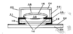
【実施例】以下、本発明の実施例であるチップタイプ温度ヒューズの実装構造について図1および図2を参照しつつ詳述する。図はプリント配線体を構成するチップ部品10とこれを搭載する実装基板30からなるチップタイプ温度ヒュ−ズの実装構造を示しており、チップ部品10はリ−ド部材11の一部を外部導出した熱可塑性の樹脂の気密パッケ−ジ20からなり、実装基板30の所定位置に搭載されて一対の配線ランド32、32間に超音波による金属間接合で電気的機械的に圧接接合される。図2に示すように、チップ部品10は気密パッケ−ジ20の内部にフラックス被膜15を被着した低融点可溶合金14のヒューズエレメント16が一対のリ−ド部材11の電極部12間に溶着して橋絡状に架設され、樹脂パッケ−ジ20の外部へ延び出る一対のリ−ド部材11の導出部13は実装基板30に形成した印刷パターンの配線ランド32、32間で超音波接合されチップタイプ温度ヒューズの実装構造を構成する。ここでリ−ド部材11はニッケル、りん青銅、鉄などの平板状導体から成り、チップ部品で配線体を自動組立するチップマンタに適合させるのが好ましい。一方、このような実装基板の所定位置へのチップ部品の供給搭載には周知のチップマウンタが使用される。したがって、本発明のチップ部品は抵抗やコンデンサ等のチップ部品と同様に処理され、自動組立作業による量産効率化に役立てられる。チップ部品が所定位置に搭載された後、一対のリ−ド部材の導出部13は超音波エネルギーが付与され、短時間のスポット的熱圧着により配線ランド32と電気的機械的な金属間接合がなされる。ここで平板状に形成されたリ−ド部材11はチップマウンタに適合する形状、例えばその導出部13をL字状にフォ−ミング加工される。更に、リ−ド部材導出部13と実装基板の配線ランド32との間にアモルファス銅、はんだチップ、印刷金属などの低融点化物質を介在することで溶着性の向上が図られる。圧接接合にはレ−ザ、電気抵抗溶接、超音波接合などの熱圧着が適用できるが、特に超音波エネルギーを付与する超音波による金属間接合が望ましい。
【0013】換言すると本発明は、一対のリード部材11間に配置したヒューズエレメント16を収納した絶縁ケースをキャップで封止した気密パッケージ20のチップ部品10と、このチップ部品が搭載される配線ランド32を有する実装基板30とから構成され、一対のリード部材11は絶縁ケースと一体成形され、この絶縁ケースの内部に電極部12と外部に導出部13を有し、実装基板30の配線ランド32と導出部13とを圧接接合したチップタイプ温度ヒューズの実装構造である。ここで、気密パッケージ20の絶縁ケ−ス22およびキャップ24がそれぞれ熱可塑性樹脂の成形体からなり、一対のリード部材11の導出部13は配線ランド32に位置決めできるようにフォーミングされ、かつ電極部12はめっき処理してヒューズエレメント16との溶着を確実容易にする。好ましくは、リ−ド部材の導出部13と実装基板の配線ランド32とは、超音波による金属間接合で圧接接合され、両者間に金属箔、印刷金属、アモルファス銅、はんだチップ等の低融点化物質を介在させて導出部と配線ランド間の電気機械的結合を容易にさせる。加えて、実装基板にはチップ部品の配置用窪み等の位置決め手段を形成し、リード部材の導出部には、接合する表面を凹凸状にすることができる。さらに、導出部13と配線ランド32との間に導電性プラスティックなどの導電性接着材を介在させてもよく、位置決めをより確実に達成させる。また、リ−ド部材はニッケル、りん青銅、鉄等の平板状導体からなり、その電極部または導出部をめっき処理して低融点可溶合金または配線ランドとの溶着を容易にし、図2に示すように、導出部13は気密パッケージ20の外周底面に沿うように配置する。
【0014】
【発明の効果】本発明によるチップタイプ温度ヒュ−ズの実装構造は、一対のリード部材の電極部間にフラックスを被着した低融点可溶合金が架設されて熱可塑性の樹脂パッケ−ジからなるチップ部品と、実装基板上の配線ランドに搭載する際超音波による圧接接合で電気機械的に結合するので配線体の組立作業においてチップマウンタによる自動供給搭載ができる。特に、チップタイプ温度ヒュ−ズの搭載においては超音波による圧接接合技術を利用するので、温度ヒューズに不具合を伴なうことなく確実かつ容易に実装作業ができる。また、超音波金属間接合の適用によりチップ部品を所定位置に確実に搭載され配線体の小型薄型化に寄与し、品質安定化と信頼性の向上に役立つなどの実用的効果が期待される。
【図面の簡単な説明】
【図1】本発明の実施例に係る温度ヒューズの実装構造を示す部分切り欠き平面図。
【図2】図1の略中央に沿った部分の要部側断面図。
【符号の説明】
10 チップ部品
11 リ−ド部材
12 電極部
13 導出部
14 低融点可溶合金
15 フラックス被膜
16 ヒューズエレメント
20 気密パッケ−ジ
22 絶縁ケ−ス
24 キャップ
30 実装基板
32 配線ランド[0001]
BACKGROUND OF THE INVENTION 1. Field of the Invention The present invention relates to a mounting structure of a chip type temperature fuse used on a mounting substrate such as a printed wiring, and more particularly, to a chip component without causing a defect in a low melting point fusible alloy fuse element. The present invention relates to a mounting structure of an alloy type chip type thermal fuse mounted at a predetermined position on a mounting substrate.
[0002]
2. Description of the Related Art A thermal fuse for applying a flux to a low-melting-point fusible alloy to make the fusible alloy into a spherical shape at the time of melting is formed by welding and joining a low-melting-point fusible alloy between a pair of lead tip side electrodes. Be composed. The flux applied to the surface of the low-melting fusible alloy prevents the oxide film from interfering when the low-melting fusible alloy melts at the melting temperature, and forms the fusible alloy melted at a predetermined temperature into a spherical shape by surface tension. The electrical connection between the two electrode portions can be used for disconnection (see JP-A-06-243767 and JP-A-04-282523).
On the other hand, wiring bodies used in electronic devices have recently been manufactured using a high-speed mounting technology using an automated chip mounter due to the development of miniaturized components and high-density mounting technology. For example, a chip component of less than 1 mm square is used as a circuit component in a wiring body for a mobile phone by using an automatic supply system and a mounter device. From such demands, a temperature fuse of a thin type in which a low melting point fusible alloy is surrounded by an insulating material and having a thickness of less than 1 mm and a small type in which a fusible alloy is mounted on an insulating substrate is known. See JP-A-2-291624).
[0004]
In the mounting of a chip component as a wiring body, the above-mentioned chip type temperature fuse is provided with a lead lead-out portion extending outside the hermetic package. Solder mounted in position. However, during the soldering process, heat from the molten solder material is transmitted into the package component through the lead, and the fuse element may be melted and disconnected. In order to avoid such thermal fuse failures, the mounting of chip components depends on individual and careful hand soldering or requires careful work. Automated mounting including soldering similar to general chip components has been considered to be unsuitable for thermal fuses made into chip components because of the problems such as disconnection defects. For this reason, it has been difficult to reduce the mounting area to be soldered in the mounting operation of the chip component.
When a chip type temperature fuse is incorporated into a printed wiring body, there is a problem in a soldering operation using a solder material which is a fusible alloy in order not to cause a defect in a fuse element. Was needed to be applied. Therefore, in order to prevent the occurrence of failure of the fuse element in handling such chip components and to always exhibit the original function of the temperature fuse satisfactorily, a method of mounting the chip components on the mounting board by a method different from soldering. The proposal was desired.
Therefore, the present invention has been proposed in view of the above-mentioned drawbacks, and when mounting a chip component having a fuse element on a mounting substrate on which wiring lands are formed, a connection error or a failure of the fuse element is required. An object of the present invention is to provide a new and improved chip-type thermal fuse mounting structure by press-welding for preventing disconnection and damage.
Another object of the present invention is to provide a new and improved chip-type thermal fuse which can reliably and quickly mount chip components mounted between wiring lands on a mounting board without deteriorating a fuse element function. It is to provide a mounting structure.
[0008]
According to the present invention, there is provided a mounting structure of a chip type thermal fuse, comprising: a mounting substrate provided with wiring lands for mounting circuit components; and a low melting point fusible alloy of a fuse element between a pair of lead members. It is provided with a chip component that is erected and has a flux coating formed on its surface and then hermetically packaged. The lead portion of the pair of lead members and the wiring land of the mounting substrate are pressure-welded and mounted on the mounting substrate.
In the mounting structure of the chip type temperature fuse of the present invention, the lead parts of the pair of lead members are connected between the wiring lands of the mounting board by resistance welding, ultrasonic bonding, thermocompression bonding or the like. It is mounted on a mounting substrate by electromechanical coupling. Preferably, a chip component positioning means is formed on the mounting substrate, the wiring land and the lead member lead-out portion are formed substantially flat to form a desired L-shape, and a material having a low melting point is interposed. The lead-out part and the wiring land are welded by metal-to-metal bonding using ultrasonic waves, and are electrically and mechanically connected.
[0010]
DESCRIPTION OF THE PREFERRED EMBODIMENTS A chip type temperature fuse according to the present invention comprises a pair of lead members each having an electrode at one end, and a fuse element having a predetermined melting temperature bridged between the two electrodes. And an insulating case, wherein the insulating case is bonded with a cap and hermetically packaged, and the fuse element is made of a low melting point soluble alloy of tin (Sn), antimony (Sb), An alloy having two or more compositions selected from metal groups including cadmium (Cd), indium (In), lead (Pb), bismuth (Bi), silver (Ag), and copper (Cu). The fusing temperature is determined within the operating temperature range of 60 to 190 ° C. depending on the composition ratio. For example, a ternary alloy material containing Sn-Pb-Bi is used for a temperature fuse having an operating temperature of 98 ° C, and a binary alloy material of Sn-Pb is used for a temperature fuse having an operating temperature of 180 ° C. .
In mounting the chip component on the mounting board, the lead-out portion of the lead member is provided between the predetermined wiring lands on the mounting board without deteriorating the fuse element function by resistance welding, friction welding, thermocompression bonding. Then, they are pressure-bonded by ultrasonic bonding or the like, and are electrically and mechanically connected. The pressure welding is desirably an ultrasonic metal-to-metal bonding, which does not cause a problem with the low melting point fusible alloy of the fuse element. In addition, at the time of this bonding, preferably, not only the bonding strength between the lead portion of the chip component and the wiring land of the mounting board is increased by interposing a low-melting substance such as amorphous copper, indium, or a solder chip, In addition, thermal damage to the mounting board can be suppressed. At this time, plating can be performed on the surface of the lead member to facilitate the joining.
[0012]
DETAILED DESCRIPTION OF THE PREFERRED EMBODIMENTS A mounting structure of a chip type thermal fuse according to an embodiment of the present invention will be described below in detail with reference to FIGS. The figure shows a mounting structure of a chip type temperature fuse including a
In other words, the present invention provides a
[0014]
The mounting structure of the chip type temperature fuse according to the present invention comprises a low melting point fusible alloy with a flux applied between the electrodes of a pair of lead members. The chip component is electrically and mechanically coupled by ultrasonic pressure bonding when mounted on a wiring land on a mounting board, so that automatic supply and mounting by a chip mounter can be performed in a wiring assembly operation. In particular, in mounting the chip type temperature fuse, the pressure welding technique using ultrasonic waves is used, so that the mounting operation can be performed reliably and easily without causing a defect in the temperature fuse. Further, application of ultrasonic metal-to-metal bonding is expected to have a practical effect such that the chip component is securely mounted at a predetermined position, which contributes to miniaturization and thinning of the wiring body, which contributes to stabilization of quality and improvement of reliability.
[Brief description of the drawings]
FIG. 1 is a partially cutaway plan view showing a mounting structure of a thermal fuse according to an embodiment of the present invention.
FIG. 2 is a side sectional view of a main part of a portion substantially along the center of FIG. 1;
[Explanation of symbols]
DESCRIPTION OF
Claims (7)
Priority Applications (1)
| Application Number | Priority Date | Filing Date | Title |
|---|---|---|---|
| JP2002174419A JP2004022290A (en) | 2002-06-14 | 2002-06-14 | Structure for mounting chip-type thermal fuse |
Applications Claiming Priority (1)
| Application Number | Priority Date | Filing Date | Title |
|---|---|---|---|
| JP2002174419A JP2004022290A (en) | 2002-06-14 | 2002-06-14 | Structure for mounting chip-type thermal fuse |
Publications (2)
| Publication Number | Publication Date |
|---|---|
| JP2004022290A true JP2004022290A (en) | 2004-01-22 |
| JP2004022290A5 JP2004022290A5 (en) | 2005-10-13 |
Family
ID=31173389
Family Applications (1)
| Application Number | Title | Priority Date | Filing Date |
|---|---|---|---|
| JP2002174419A Pending JP2004022290A (en) | 2002-06-14 | 2002-06-14 | Structure for mounting chip-type thermal fuse |
Country Status (1)
| Country | Link |
|---|---|
| JP (1) | JP2004022290A (en) |
Cited By (2)
| Publication number | Priority date | Publication date | Assignee | Title |
|---|---|---|---|---|
| JP2015035280A (en) * | 2013-08-07 | 2015-02-19 | デクセリアルズ株式会社 | Protection circuit board |
| US10032583B2 (en) | 2016-02-17 | 2018-07-24 | Dexerials Corporation | Protective circuit substrate |
-
2002
- 2002-06-14 JP JP2002174419A patent/JP2004022290A/en active Pending
Cited By (2)
| Publication number | Priority date | Publication date | Assignee | Title |
|---|---|---|---|---|
| JP2015035280A (en) * | 2013-08-07 | 2015-02-19 | デクセリアルズ株式会社 | Protection circuit board |
| US10032583B2 (en) | 2016-02-17 | 2018-07-24 | Dexerials Corporation | Protective circuit substrate |
Similar Documents
| Publication | Publication Date | Title |
|---|---|---|
| KR100629826B1 (en) | Compound and circuit device using the same | |
| JPH077038A (en) | Electronic package | |
| JP7231527B2 (en) | Fuse element for protection element and protection element using the same | |
| CN111540597B (en) | Coil component and method for manufacturing same | |
| JP2006269970A (en) | Solder joint method of electronic component | |
| JP2004165637A (en) | Semiconductor device | |
| JP2004179551A (en) | Coil apparatus and method of manufacturing the same | |
| JP3702117B2 (en) | Electronic component equipment | |
| JP2004273401A (en) | Electrode connecting member, circuit module using it and manufacturing method therefor | |
| WO2010070779A1 (en) | Anisotropic conductive resin, substrate connecting structure and electronic device | |
| JP2004022290A (en) | Structure for mounting chip-type thermal fuse | |
| US20040262644A1 (en) | Hybrid integrated circuit device | |
| JP2637863B2 (en) | Semiconductor device | |
| JP2003288827A (en) | Chip type temperature fuse and its mounting structure | |
| JP4002117B2 (en) | Multilayer substrate and manufacturing method thereof | |
| CN101355065A (en) | Semiconductor device having external connection terminals and method of manufacturing the same | |
| JP2633745B2 (en) | Semiconductor device package | |
| JP3225936B2 (en) | Inductance element and method of manufacturing the same | |
| JP2002368038A (en) | Flip-chip mounting method | |
| JP2002043466A (en) | Ball grid array package | |
| JP2002271005A (en) | Mounting structure and method of manufacturing the same | |
| JP2002246261A (en) | Resin sealed electronic device | |
| JPH10200307A (en) | Nonreversible circuit element | |
| US20060244110A1 (en) | Electronic device | |
| JP2004096029A (en) | Manufacturing method of power semiconductor device |
Legal Events
| Date | Code | Title | Description |
|---|---|---|---|
| A521 | Written amendment |
Free format text: JAPANESE INTERMEDIATE CODE: A523 Effective date: 20050531 |
|
| A621 | Written request for application examination |
Effective date: 20050531 Free format text: JAPANESE INTERMEDIATE CODE: A621 |
|
| A131 | Notification of reasons for refusal |
Free format text: JAPANESE INTERMEDIATE CODE: A131 Effective date: 20080222 |
|
| A02 | Decision of refusal |
Free format text: JAPANESE INTERMEDIATE CODE: A02 Effective date: 20080626 |