JP2004006659A - Semiconductor laser device - Google Patents
Semiconductor laser device Download PDFInfo
- Publication number
- JP2004006659A JP2004006659A JP2003036142A JP2003036142A JP2004006659A JP 2004006659 A JP2004006659 A JP 2004006659A JP 2003036142 A JP2003036142 A JP 2003036142A JP 2003036142 A JP2003036142 A JP 2003036142A JP 2004006659 A JP2004006659 A JP 2004006659A
- Authority
- JP
- Japan
- Prior art keywords
- semiconductor laser
- heat sink
- laser device
- groove
- laser element
- Prior art date
- Legal status (The legal status is an assumption and is not a legal conclusion. Google has not performed a legal analysis and makes no representation as to the accuracy of the status listed.)
- Pending
Links
Images


Abstract
Description
【0001】
【発明の属する技術分野】
本発明は、CD,CD−R/RW,DVD,DVD−R/RW,DVD−ブルーレイディスク等の光ディスク用光源に使用することができる半導体レーザ装置に関する。特に、光ディスク用のスリム(薄型)なピックアップ用に適した小型パッケージを備える半導体レーザ装置、あるいはそのパッケージに関する。
【0002】
【従来の技術】
現行のハーフハイトピックアップには、φ5.6mmステムを有する半導体レーザ装置が使用されている。スリムピックアップにはφ5.6mmステムの一部をカットしたD型ステム、両方をカットしたI型ステムのパッケージなどが提案されている。また、φ3.5mmステム、φ3.3mmステムのパッケージも提案されている(図13に示す外観参照)。このφ3.5mmステム、φ3.3mmステムは、図13に外観を示すようにφ5.6mmステムパッケージを全体的に縮小した形であるため、レーザ素子配置用のヒートシンク部が小さくなるという問題がある。またヒートシンク部の体積を大きくした内容で特許文献1などが知られているが、これは半円状で体積的には不充分である。
【0003】
CD−R、DVD−R用等の高出力タイプの半導体レーザ装置の場合、電流値,電圧ともに大きくなり、それに伴い発熱が増加しφ3.3mmステムのような放熱体積の小さいステムでは70℃以上の高温保証が困難になるという問題点があった。したがって、如何に放熱体積を稼ぐかが重要になってくる。
【0004】
【特許文献1】
特開平10−362032号公報
【0005】
【発明が解決しようとする課題】
本発明の課題は、以下の内の1つ、あるいはそれらを組み合わせたものである。すなわち、放熱性を改善すること。パッケージの小型化を図ること。素子の保護を図ること。リードピン数の削減を図ること。
【0006】
【課題を解決するための手段】
本発明は、請求項1に記載のように、円柱状のヒートシンク部の軸方向にそって溝を形成し、この溝の内壁面に半導体レーザ素子を配置したことを特徴とする。
【0007】
本発明は、請求項2に記載のように、円状のベース部とヒートシンク部からなるパッケージの前記ヒートシンク部に半導体レーザ素子を配置した半導体レーザ装置において、前記ヒートシンク部を前記ベース部と同心円状の円柱形状とし、このヒートシンク部の軸方向にそって溝を形成し、この溝の内壁面に前記半導体レーザ素子を配置したことを特徴とする。
【0008】
本発明は、請求項3に記載のように、前記溝は、前記円柱状ヒートシンク部の中心軸を含むような深さにされていることを特徴とする。
【0009】
本発明は、請求項4に記載のように、前記溝は、前記半導体レーザ素子を完全に収納する形状に形成されていることを特徴とする。
【0010】
本発明は、請求項5に記載のように、前記溝は、前記半導体レーザ素子とそれに対するワイヤボンド線を完全に収納する形状に形成されていることを特徴とする。
【0011】
本発明は、請求項6に記載のように、前記溝は、その両側に位置する壁部が前記半導体レーザ素子よりも高い位置まで延びていることを特徴とする。
【0012】
本発明は、請求項7に記載のように、前記溝は、前記ヒートシンク部の円弧面を中心角度に換算して180度以下の範囲で切り取った形状で形成されていることを特徴とする。
【0013】
本発明は、請求項8に記載のように、一端が前記ベース部を貫通するリードピンを備え、このリードピンの一端を前記溝内に配置したことを特徴とする。
【0014】
本発明は、請求項9に記載のように、一端が前記ベース部を貫通する2本のリードピンを備え、これら2本のリードピンの一端を前記溝内に配置したことを特徴とする。
【0015】
本発明は、請求項10に記載のように、前記ヒートシンク部の先端外周部にテーパー面を形成したことを特徴とする。
【0016】
本発明は、請求項11に記載のように、前記ヒートシンク部の先端を球状面を形成したことを特徴とする。
【0017】
本発明は、請求項12に記載のように、前記ヒートシンク部の底面を平坦面としたことを特徴とする。
【0018】
本発明は、請求項13に記載のように、前記ヒートシンク部の前端面に平板状の光学素子を付加したことを特徴とする。
【0019】
本発明は、請求項14に記載のように、前記ヒートシンク部の前端面に球状の光学素子を付加したことを特徴とする。
【0020】
本発明は、請求項15に記載のように、前記ベース部と前記ヒートシンク部を同一の金属によって構成したことを特徴とする。
【0021】
本発明は、請求項16に記載のように、柱状のヒートシンク部に半導体レーザ素子を完全に収容する深さを有する溝を形成し、この溝の底部に半導体レーザ素子を配置したことを特徴とする。
【0022】
本発明は、請求項17に記載のように、半導体レーザ素子と、前記半導体レーザ素子の光軸と平行で前記半導体レーザ素子を配置するための平坦面を有する柱状のヒートシンク部とを備え、前記ヒートシンク部は、前記平坦面の前記光軸に対して左右方向の一方の側に壁部を一体に設け、この壁部の頂上部を前記半導体レーザ素子及びこの半導体レーザ素子に対するワイヤボンド線よりも高い位置としたことを特徴とする。
【0023】
【発明の実施の形態】
以下本発明の実施形態について図面を参照して説明する。
【0024】
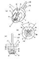
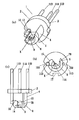
図1は、本発明の半導体レーザ装置の第1の実施形態を示し、同図(a)は斜視図、同図(b)は正面図、同図(c)は平面図である。
【0025】
半導体レーザ装置1は、ステムタイプのパッケージ2を備えている。このパッケージ2は、ベース部3とヒートシンク部4によって構成している。
【0026】
ベース部3は、直径が3.3mm、厚さが1mmの円盤を基本形態とした円盤状の金属で構成している。ヒートシンク部4は、直径が2.9mm、長さが2.5mmの円柱を基本形態としてその一部を切り欠いてくぼみを形成した柱状の金属で構成している。ベース部3とヒートシンク部4は、正面から見てその中心が一致するように同心円状に配置している。ベース部3とヒートシンク部4の中心Xは、後述する半導体素子の光軸Xと一致するように設定される。
【0027】
ヒートシンク部4は、円柱の中心軸方向に延びる溝5を、円柱の上平坦面と下平坦面を横切ように形成することによって、正面U字形状をしている。溝5は、その上端の幅が1.5mm、下端の幅が1.0mmと上広がりの形態で形成されている。溝5は、この溝5によって切り取られた円柱の円弧部分(溝5の上端が弦と見なされる円弧部分)が、円柱の中心軸に対する中心角度に換算して180度よりも小さな角度θになるように形成されている。この角度θは、90度よりも小さい角度に設定しているが、180度以下であれば、90度よりも大きな角度に設定しても良い。溝5は、その底面が円柱の中心軸Xよりも深い位置になる様に形成されている。溝5の底に位置する面6は、円柱の中心軸Xと平行な平坦面とされ、この平坦面6が後述する半導体レーザ素子を配置する面となる。
【0028】
ヒートシンク部4は、平坦面6の両側(前記軸Xに対して左右方向の側)に壁部7を一体に設けている。すなわち、溝5の左右に、溝5の底部の平坦面6よりも高い左右の壁部7A,7Bを有している。この壁部7A,7Bの間に後述する素子9が配置される。
【0029】
ヒートシンク部4は、その基端がベース部3に一体化されている。ベース部3とヒートシンク部4は、それぞれを別部材とし、半田などの接続材料によって両者を一体に接合してパッケージ2とすることもできるし、それぞれを同一部材とし一体成形してパッケージ2とすることもできる。ベース部3とヒートシンク部4をそれぞれを別部材とする場合は、ベース部3を熱抵抗が小さな銅あるいは銅系の合金、あるいは鉄あるいは鉄系の合金で構成するのが好ましく、ヒートシンク部4を熱抵抗が小さな銅あるいは銅系の合金で構成するのが好ましい。また、ベース部3とヒートシンク部4を一体に形成する場合は、ベース部3とヒートシンク部4を熱抵抗が小さな銅あるいは銅系の合金で構成するのが好ましい。ベース部3とヒートシンク部4を一体に形成する場合は、両者を板材のプレス加工によって、あるいは、柱材の切削加工によって同時に形成することができる。
【0030】
ヒートシンク部4は、その先端が先細りになるように、先端部の外周部にテーパー面8を形成している。このようなテーパー面8を形成することにより、通常アルミニウムなどで構成される光ピックアップ側のレーザ装置の受け入れ部分がエッジによって削られることを未然に防止することができる。
【0031】
また、ヒートシンク部4の外周部は、左右の壁部7A,7Bを含めて軸Xを中心とした円弧からなる曲面としているので、光ピックアップ側のレーザ装置の受け入れ部分の中で軸Xを中心に回転して位置調整する際、この外周曲面をガイドとすることによって調整時の動きをスムーズにすることができる。
【0032】
半導体レーザ装置1は、パッケージ部2に、半導体素子としての半導体レーザ素子9を配置している。半導体レーザ素子9は、ヒートシンク部4の取付面、この例では溝5の内壁面を構成する平坦面6にサブマウント10を介して配置している。半導体レーザ素子9は、その発光点がサブマウント10側に偏った配置、すなわちジャンクションダウンの形態で配置するのが、放熱性を高める上で好ましい。
【0033】
半導体レーザ装置1は、半導体レーザ素子9として赤外タイプから紫外タイプまで種々のものを用いることができる。特に、赤外タイプに比べて放熱特性が悪く、良好な放熱環境が要求される赤色タイプや青色タイプの半導体レーザ素子を用いるのが、その放熱特性を改善することができる点で好ましい。
【0034】
サブマウント10は、放熱性の良い部材で構成され、例えばシリコンや窒化アルミニウムなどの半導体材料を用いることができる。半導体レーザ素子9の放熱性をより高める場合などには、半導体レーザ素子9をサブマウント10を介在せずに直接ヒートシンク部4の取り付け面に取付けることもできる。
【0035】
半導体レーザ素子9は溝5内に配置され、半導体レーザ素子9の高さよりも十分に高い壁部7A,7Bに挟まれた形態で配置されているので、この壁部が素子の保護機能を果たす。
【0036】
半導体レーザ装置1は、複数のリードピン11A、11Bをパッケージ2に固定して備えている。この実施形態では、2本のリードピン11A,11Bをベース部3の中心Xを挟む様にして配置している。一方のリードピン11Aは、その一端がベース部3に溶接等によって接合されて、ベース部3に電気的に導通した状態で固定されている。他方のリードピン11Bはその一端がベース部3の貫通孔12に挿入され、この貫通孔12に配置した絶縁材13によってベース部3と絶縁された状態で固定されている。このリードピン11Bの一端は、ベース部3を貫通して溝5の中に位置している。
【0037】
一方のリードピン11Aは、ベース部3、ヒートシンク部4、ワイヤボンド線14等を介して半導体レーザ素子9の一方の電極に接続される。他方のリードピン11Bは、その一端に接続したワイヤボンド線15、サブマウント10上の配線等を介して半導体レーザ素子9の他方の電極に接続される。このリードピン11A,11B間に半導体レーザ素子9の駆動に必要な電圧を与えると、半導体レーザ素子9が動作してレーザ光が軸X方向に出力される。
【0038】
各ワイヤボンド線14,15は、側壁7A,7Bによる保護を受けるために、溝5の上縁からはみ出さない様に、溝5内に配置するのが好ましい。すなわち、溝5は、半導体レーザ素子9、サブマウント10、各ワイヤボンド線14,15を完全に収納するような形状に形成されている。
【0039】
半導体レーザ装置1は、従来と同様に、位置決め用の一対の三角形状の切り欠き16A,16Bと、方向表示用の四角形状の切り欠き17をベース部3に備えている。
【0040】
この半導体レーザ装置1は、図1に示す状態が完成状態であり、光ピックアップ装置等にその光源として組み込まれて使用される。このとき、ヒートシンク部4の先端がテーパー面8となっているので、このレーザ装置1を装着個所にスムーズに差し込むことができる。また、テーパー面8を先端に形成することにより、通常アルミニウムなどで構成される光ピックアップ側のレーザ装置の受け入れ部分がエッジによって削られることを防止することができる。したがって、エッジによって削られて発生する金属粉が光学系に与える悪影響を未然に防止することができる。光ピックアップ装置等に組み込まれて使用されるとき、ベース部3のヒートシンク部4側の平坦面が、位置決め用の基準面として機能する。
【0041】
図1に示す実施形態において、ヒートシンク部4の体積は11.1mm3であり、図10に示す従来タイプ(φ3.5mm)の1.1mm3の約10倍に増加することができた。パッケージ2の全体体積(ベース部3とヒートシンク部4の合計体積)は、20.7mm3であり、図13に示す従来タイプの10.7mm3の約2倍に増加することができた。ヒートシンク部4のパッケージ2の全体積に占める体積割合は約53%(11.1/20.7)で、図13に示す従来タイプの約10%(1.1/10.7)に比べて約5倍に増加することができた。したがって、半導体レーザ素子9から発生する熱を効果的に放熱することができる。
【0042】
図12は、赤色半導体レーザ素子を有するDVD−R用の半導体レーザ装置において、70℃の環境下で100mWのパルス試験を行なった場合の信頼性試験の結果を示す。横軸は時間、縦軸はAPC(オートパワーコントロール)下での動作電流を示す。この図から明らかなように、図13に示す従来構造では100時間前後で素子が動作不能な状態になるのに対して、本発明の実施形態では、500時間以上安定して動作することを確認できた。
【0043】
上記実施形態においては、従来のキャップによる気密構造は採用していないので部品点数、組立て工数を削減することができる。また、ヒートシンク部4が外気と触れる面積も増加させることができる。
【0044】
尚、図1に示す構造に加えて、従来のように窓付きのキャップを密閉状態で装着して半導体レーザ装置を構成することも可能である。
【0045】
図1に示す半導体レーザ装置1は、受光素子を内臓していないので、半導体レーザ素子9の出力をモニターするためには、フロントモニター用の受光素子をレーザ装置1とは別個に配置することが好ましい。
【0046】
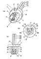
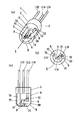
次に、本発明の第2の実施形態を図2を参照して説明する。図1に示す実施形態と同一構成要素については同一の符号を示してその説明を省略し、相違点を中心に説明する。第1の実施形態と大きく相違するのは、サブマウント10として受光素子18を内臓したタイプのものを用いた点、その出力を取り出すために、リードピンを1本増加して3本とした点である。
【0047】
ベース部3には、2本のリードピン11B,11Cを貫通配置するに十分な大きさを有する横方向に長い1つの貫通孔12が形成されている。この孔12に2本のリードピン11B,11Cをそれらの一端が溝5内に位置するように、互いに離間して配置している。この2本のリードピン11B,11Cは、絶縁材13によって互いに絶縁され、さらにベース部3とも絶縁されて固定されている。リードピン11Bの一端は、先の実施形態と同様に、半導体レーザ素子9に対する配線に利用され、もう1つのリードピン11Cは、サブマウント10に内臓の受光素子18に対する配線に利用される。受光素子18は、PIN型の受光素子で2端子構造とされ、一方の端子に接続した電極(この例では裏面電極)が、ヒートシンク部4に電気的に接続され、他方の電極(この例では表電極)が、リードピン11Cにワイヤボンド線19を介して接続される。
【0048】
第2の実施形態においても、第1の実施形態と同様の作用効果を奏することができる。さらに、受光素子内蔵型の半導体レーザ装置であっても、ベース部3を貫通するリードピン11B、11Cの先端を溝5内に配置し、溝5の中でワイヤボンド配線をすることができるので、受光素子18に対する配線をヒートシンク部4によって確実に保護することができる。また、パッケージ2の小型化を図ることができる。
【0049】
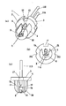
次に、本発明の第3の実施形態を図3を参照して説明する。図1に示す実施形態と同一構成要素については同一の符号を示してその説明を省略し、相違点を中心に説明する。第1の実施形態と大きく相違するのは、ヒートシンク部4の先端をテーパー面8から半球状の曲面20にした点である。半導体レーザ素子9やサブマウント10は、この曲面20よりも前方に出ないように配置されている。このように曲面20を形成することによって、半導体レーザ装置1の先端がボールペンの先端と同様の形態となり、ピックアップ装置等に組み込む際のあおり調整が行ないやすくなる。すなわち、レーザ装置の先端をピックアップ装置の半球状のくぼみに配置し、光軸が最適位置に来るようにリードピン側をX−Y方向に移動しながら調整する、あおり調整と呼ばれる調整を容易にすることができる。
【0050】
この第3の実施形態において、半導体レーザ素子9の位置を図3に示す状態から軸X方向に沿って前後(例えばベース部3側)に若干移動した状態に変更することもできる。例えば、半導体レーザ素子9をその光出射点が曲面20から等距離になる様に配置することができる。すなわち、曲面20を1つの球の一部とみなした時、その球の中心に半導体レーザ素子9の光出射点が位置するように、半導体レーザ素子9を配置する。このように配置することにより、前記あおり調整の際に、半導体レーザ素子9の光出射点が移動しなくなる。その結果、調整作業が容易になる。
【0051】
この第3の実施形態は、第2の実施形態や後述するその他の実施形態に適用することができる。
【0052】
次に、本発明の第4の実施形態を図4を参照して説明する。図1に示す実施形態と同一構成要素については同一の符号を示してその説明を省略し、相違点を中心に説明する。第1の実施形態と大きく相違するのは、ヒートシンク部4の形状を変更した点である。第1の変更点は、溝5の平坦面6先端に下向きに傾斜したテーパー面21を形成した点である。このようなテーパー面21を形成することにより、半導体レーザ素子9から出力される光が溝5の平坦面6によって遮られるのを防止することができる。テーパー面21の角度は、半導体レーザ素子9の光の上下方向への広がり角度の半分よりも大きな角度に設定する。半導体レーザ素子9の光の上下方向への広がり角度は、通常30度程度であるので、テーパー面21の傾斜角度は、15度以上に設定でき、例えば15度から20度の範囲の角度に設定される。
【0053】
素子9の位置を同じに保ったまま、ヒートシンク部4の長さを長くする場合などにおいて、素子の前方にテーパー面21を形成しておくことにより、ヒートシンク部4の長さを長く設定し易くなる。したがって、ヒートシンク部4の体積を増加することができ、放熱面積を広くすることができる。
【0054】
第2の変更点は、ヒートシンク部5の円弧面であった底面を平坦な底面22とした点である。この底面22は、溝5の平坦面6と平行な平坦面で、平坦面6よりも大きな面積としている。このような平坦な底面22としたことにより、半導体レーザ素子9等へのワイヤボンド作業時にパッケージ2を安定して支えることができるようになる。
【0055】
上記第1、第2の変更点は各々別々に行なっても良いし、同時に行なっても良い。
【0056】
この第4の実施形態は、第2、第3の実施形態や後述するその他の実施形態に適用することができる。
【0057】
次に、本発明の第5の実施形態を図5を参照して説明する。図1に示す実施形態と同一構成要素については同一の符号を示してその説明を省略し、相違点を中心に説明する。第1の実施形態と大きく相違するのは、ヒートシンク部4の形状を変更した点と、その先端に光学素子23を付加した点である。
【0058】
第1の変更点は、ヒートシンク部4の先端に設けていたテーパー面8の形成を行なわないで、円柱状のままとした点、すなわち、ヒートシンク部4の先端面と後端面とを同一平面形状とした点である。このようにヒートシンク部4の先端形状を設定することにより、ヒートシンク部4の先端面24の面積を広く確保することができる。したがって、ヒートシンク部4の先端面24に光学要素23を付加する際の取り付け代を広くすることができる。
【0059】
第2の変更点は、ヒートシンク部4の先端部に光学要素23を付加した点である。この光学要素23は、平板状をしているが、少なくともヒートシンク部4側の面が平坦な形状をしていればよい。例えば、光学要素23のヒートシンク部4側の面と反対側の面に、前記テーパー面8に相当するようなテーパー面を形成しても良い。光学要素23としては、ホログラム素子、1/4波長板、偏光板、板状レンズなどの中から選択した1つを用いることができる。半導体レーザ装置とは別個に設けていた光学要素23を一体に設けたので、光ピックアップや光通信用の送信機などにおける光学的な調整が簡素化できる。
【0060】
上記の第1、第2の変更点は各々別々に行なっても良いし、同時に行なっても良い。
【0061】
この第5の実施形態は、第2、第4の実施形態や後述するその他の実施形態に適用することができる。
【0062】
次に、本発明の第6の実施形態を図6を参照して説明する。図2に示す実施形態と同一構成要素については同一の符号を示してその説明を省略し、相違点を中心に説明する。第2の実施形態と大きく相違するのは、ヒートシンク部4の形状を変更した点と、その先端に光学素子25を付加した点である。
【0063】
第1の変更点は、ヒートシンク部4の先端にその外側に設けていたテーパー面8の形成を行なわないで、円柱状のままとし、溝5の先端に光学素子25を受け入れるくぼみを設けた点である。このようにヒートシンク部4の先端形状を設定することにより、球状の光学要素25を確実に取りつけることができる。
【0064】
第2の変更点は、ヒートシンク部4の先端部に球状の光学要素25を付加した点である。この光学要素25は、半導体レーザ素子9の発する光をコリメートし、あるいは集光するために用いられる。そして要素25はヒートシンク部4の先端部に設けたくぼみに保持され、接着剤などによって固定される。半導体レーザ装置とは別個に設けていた光学要素25を光学的な調整を行なって一体に設けたので、光ピックアップや光通信用の送信機、光ファイバーモジュールなどに適用する場合に、その光学的な調整が簡素化できる。
【0065】
上記の第1、第2の変更点は各々別々に行なっても良いし、同時に行なっても良い。
【0066】
この第6の実施形態は、第1、第4の実施形態やその他の実施形態に適用することができる。
【0067】
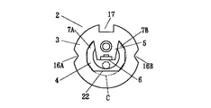
次に、本発明の第7の実施形態を図7を参照して説明する。図1に示す実施形態と同一構成要素については同一の符号を示してその説明を省略し、相違点を中心に説明する。第1の実施形態と大きく相違するのは、ヒートシンク部4の円弧状側面形状を多面形状に変更した点である。正面から見て、円弧部分を備えていたヒートシンク部4の外周部を、正面から見て多角形状に変更した。多角形に変更することによって、チャッキングが容易に行なえるようになる。ヒートシンク部4の円弧面であった底面は、第4の実施形態と同様に平坦な底面22としている。この底面22は、溝5の平坦面6と平行な平坦面で、平坦面6よりも大きな面積としている。このような平坦な底面22としたことにより、半導体レーザ素子9等へのワイヤボンド作業時にパッケージ2を安定して支えることができるようになる。
【0068】
ヒートシンク部4は、それを円筒状を成すくぼみの中に挿入した際、その取り付け安定性を高めるために、周囲の面の複数の角部分が仮想の円筒(図7に一点鎖線Cで示す)に内接するように形成している。この時、仮想の円筒Cの中心軸は前記軸Xと一致する。
【0069】
この第7の実施形態は、第2の実施形態やその他の実施形態に適用することができる。
【0070】
次に、本発明の第8の実施形態を図8を参照して説明する。図1に示す実施形態と同一構成要素については同一の符号を示してその説明を省略し、相違点を中心に説明する。第1の実施形態と大きく相違するのは、ベース部3とヒートシンク部4の形状を変更した点である。
【0071】
第1の変更点は、ベース部3とヒートシンク部4との外形寸法の相違によって形成され、位置決め基準面として用いられていた段差、すなわち、ヒートシンク部4の周囲からはみ出しているベース部3の外周部をなくした点である。このようにベース部3とヒートシンク部4を一体の円柱形状とし、その間の段差を無くしたことにより、半導体レーザ装置を軸X方向に移動させて取付け調整する際、前記段差によって受ける規制が無くなり、調整作業が容易になる。
【0072】
第2の変更点は、ワイヤボンドの作業性を高めるために、ヒートシンク部4の壁部7Bの一部を除去し、平坦面6Bを設けた点である。平坦面6Bは、溝5の平坦面6と同一平面としているが、溝5の底面5と段差を持った平坦面としても良い。このような平坦面6Bを形成することにより、素子9あるいはサブマウント10に対してワイヤボンドを行なうためのキャピラリの形状が制約を受けにくくなり、製造時の作業性を良好にすることができる。
【0073】
上記第1、第2の変更点は各々別々に行なっても良いし、同時に行なっても良い。
【0074】
この第8の実施形態は、第2から第7の何れかの実施形態やその他の実施形態に適用することができる。
【0075】
次に、本発明の第9の実施形態を図9を参照して説明する。図1に示す実施形態と同一構成要素については同一の符号を示してその説明を省略し、相違点を中心に説明する。第1の実施形態と大きく相違するのは、ダミーのリードピン11Dを設けて、一般的な3ピンの装置とピンコンパチブルにした点、溝5の左右に形成していた左右の壁部7A,7Bの一方を削除して平坦な面6の左右の一方のみに壁部7Bを形成した点である。
【0076】
ヒートシンク部4は、壁部7A,7Bの一方を削除することによって、正面から見てL字形状としている。先の実施例では、溝5の底面を構成する平坦面6に半導体レーザ素子9を配置するとしたが、この実施例のように溝5の形状を扇型(V字状)と見なすことができる場合は、溝5の一方の内壁面に半導体レーザ素子9が配置されていると見なすこともできる。
【0077】
リードピン11Bは、溝5に完全に収容されるのではなく、一部が溝5からはみ出した状態でベース部3に絶縁されて固定されている。ダミーのリードピン11Dは、リードピン11Aと同様に、その一端がベース部3に溶接などによって接合されて、ベース部3に電気的に導通した状態で固定されている。リードピン11Dは、リードピン11Aと同様に軸X方向から見てヒートシンク部4と平面的に重なる位置に配置される。リードピン11Dは、一般的な3ピンの装置において、モニター信号出力用のリードピンが配置される位置と同じ位置に配置される。したがって、一般的な3ピンの装置とピン配置がコンパチブルになり、共通の製造装置を利用して製造することが可能になる。
【0078】
モニター機能内蔵型の装置は、モニター信号出力用のリードピンを、リードピン11Bと同様に、ヒートシンク部4との平面的な重なりを避けて配置する必要があるので、ヒートシンク部4の設置個所が限定される。しかしながら、この実施例の場合は、リードピン11Dがベース部3から突出しないダミーリードであるため、ヒートシンク部4の設置可能範囲を広く確保することができる。すなわち、本来ならがモニター信号出力用のリードピンが位置する範囲にヒートシンク部4、この例では壁部7Bを突出して配置することができる。
【0079】
その結果、通常は面6と同じ位置であるヒートシンク部4の上端位置を、半導体レーザ素子9の発光点もしくは上面よりも上の位置まで突出して配置することができる。このように発光点もしくは上面よりも上の位置まで突出する壁部7Bの存在によって、放熱のための体積、あるいは表面積を増加させることができ、放熱性を良好にすることができる。
【0080】
この第9の実施形態は、第2から第8の何れかの実施形態やその他の実施形態に適用することができる。
【0081】
次に、本発明の第10の実施形態を図10を参照して説明する。図9に示す実施形態と同一構成要素については同一の符号を示してその説明を省略し、相違点を中心に説明する。第9の実施形態との相違点は、ヒートシンク部4の壁部7の形状を変更した点である。すなわち、鋭角であった壁部7の頂上部を面取りして平坦面7Cとした。このような構成によって、第9の実施形態よりも放熱性の点で若干劣るが、第9の実施形態と同様の効果を奏することができる。
【0082】
次に、本発明の第11の実施形態を図11を参照して説明する。この実施形態は、図8に示す実施形態をベースとして、図9、10に示す実施形態を付加したものである。したがって、図8〜10に示す実施形態と同一構成要素については同一の符号を示している。
【0083】
ベース部3とヒートシンク部4は、両者の間に段差が生じないように同一の直径とされている。円柱形状の一部が切り欠かれてヒートシンク部4とされ、切り欠かれなかった部分がベース部3とされている。このようにベース部3とヒートシンク部4を一体の円柱形状とし、その間の段差を無くしたことにより、半導体レーザ装置を軸X方向に移動させて取付け調整する際、前記段差によって受ける規制が無くなり、調整作業が容易になる。
【0084】
絶縁材によってベースに固定されたリードピン11Bの一端は、ベース部3を貫通して平坦面6Bの上方まで延びている。リードピン11Dは、リードピン11Aと同様に、その一端がベース部3に溶接などによって接合されて、ベース部3に電気的に導通した状態で固定されている。リードピン11Dは、リードピン11Aと同様に軸X方向から見てヒートシンク部4と平面的に重なる位置に配置される。リードピン11Dは、一般的な3ピンの装置において、モニター信号出力用のリードピンが配置される位置と同じ位置に配置される。したがって、一般的な3ピンの装置とピン配置がコンパチブルになり、共通の製造装置を利用して製造することが可能になる。壁部7は、頂上部を面取りして平坦面7Cを形成している。
【0085】
この第11の実施形態によれば、第8〜10の実施形態における効果と同様の効果を奏することができる。
【0086】
上記実施形態において、半導体レーザ素子9に代わる半導体発光素子として発光ダイオードを用いることもできる。それ以外にも、本発明の趣旨を変更しない範囲であれば、上記実施形態以外の変更を行なっても良い。
【0087】
【発明の効果】
以上のように本発明によれば、半導体レーザ装置の放熱性を高めることができる。また、別の局面では、パッケージの小型化を図ることができる。また、別の局面では、素子の保護を図ることができる。また、別の局面ではリードピン数の削減を行なうことができる。
【図面の簡単な説明】
【図1】本発明の第1の実施形態を示し、(a)は斜視図、(b)は正面図、(c)は平面図である。
【図2】本発明の第2の実施形態を示し、(a)は斜視図、(b)は正面図、(c)は平面図である。
【図3】本発明の第3の実施形態を示し、(a)は斜視図、(b)は正面図、(c)は平面図である。
【図4】本発明の第4の実施形態を示し、(a)は一部切り欠き側面図、(b)は正面図である。
【図5】本発明の第5の実施形態を示し、(a)は平面図、(b)は正面図である。
【図6】本発明の第6の実施形態を示す平面図である。
【図7】本発明の第7の実施形態を示す正面図である。
【図8】本発明の第8の実施形態を示す斜視図である。
【図9】本発明の第9の実施形態を示し、(a)は斜視図、(b)は正面図、(c)は平面図である。
【図10】本発明の第10の実施形態を示し、(a)は斜視図、(b)は正面図、(c)は平面図である。
【図11】本発明の第11の実施形態を示し、(a)は斜視図、(b)は正面図、(c)は平面図である。
【図12】信頼性試験のデータを示す特性図である。
【図13】従来例を示す一部切り欠き斜視図である。
【符号の説明】
1 半導体レーザ装置
2 パッケージ
3 ベース部
4 ヒートシンク部
5 溝
9 半導体レーザ素子(半導体発光素子)
11 リードピン[0001]
TECHNICAL FIELD OF THE INVENTION
The present invention relates to a semiconductor laser device that can be used as a light source for an optical disk such as a CD, a CD-R / RW, a DVD, a DVD-R / RW, and a DVD-Blu-ray disk. In particular, the present invention relates to a semiconductor laser device including a small package suitable for a slim (thin) pickup for an optical disk, or a package thereof.
[0002]
[Prior art]
A semiconductor laser device having a φ5.6 mm stem is used for the current half-high topic up. As a slim pickup, a package of a D-type stem in which a part of a φ5.6 mm stem is cut, an I-type stem in which both are cut, and the like have been proposed. Further, packages of a φ3.5 mm stem and a φ3.3 mm stem have been proposed (see the external appearance shown in FIG. 13). As shown in FIG. 13, the φ3.5 mm stem and the φ3.3 mm stem have a reduced size of the φ5.6 mm stem package as a whole. . Further,
[0003]
In the case of a high-output type semiconductor laser device for CD-R, DVD-R, etc., both the current value and the voltage are increased, and accordingly, heat generation is increased. However, there is a problem that it is difficult to guarantee the high temperature of the device. Therefore, how to increase the heat radiation volume becomes important.
[0004]
[Patent Document 1]
JP-A-10-362032
[0005]
[Problems to be solved by the invention]
The object of the present invention is one of the following or a combination thereof. That is, heat dissipation is improved. Reduce the size of the package. To protect the device. Reduce the number of lead pins.
[0006]
[Means for Solving the Problems]
According to the present invention, a groove is formed along the axial direction of the columnar heat sink portion, and a semiconductor laser element is disposed on an inner wall surface of the groove.
[0007]
According to a second aspect of the present invention, in a semiconductor laser device in which a semiconductor laser element is disposed on the heat sink portion of a package including a circular base portion and a heat sink portion, the heat sink portion is concentric with the base portion. And a groove is formed along the axial direction of the heat sink portion, and the semiconductor laser element is disposed on the inner wall surface of the groove.
[0008]
According to a third aspect of the present invention, the groove has a depth including a central axis of the cylindrical heat sink.
[0009]
According to a fourth aspect of the present invention, the groove is formed in a shape that completely accommodates the semiconductor laser device.
[0010]
According to a fifth aspect of the present invention, the groove is formed in a shape that completely accommodates the semiconductor laser element and a wire bond line for the semiconductor laser element.
[0011]
According to a sixth aspect of the present invention, in the groove, the wall portions located on both sides of the groove extend to a position higher than the semiconductor laser element.
[0012]
According to a seventh aspect of the present invention, the groove is formed in a shape in which the arc surface of the heat sink portion is cut in a range of 180 degrees or less in terms of a center angle.
[0013]
According to the present invention, as set forth in
[0014]
According to a ninth aspect of the present invention, one end includes two lead pins penetrating the base portion, and one end of each of the two lead pins is disposed in the groove.
[0015]
According to a tenth aspect of the present invention, a tapered surface is formed on an outer peripheral portion of a distal end of the heat sink portion.
[0016]
The present invention is characterized in that the tip of the heat sink has a spherical surface as described in claim 11.
[0017]
According to another aspect of the present invention, the bottom surface of the heat sink portion is a flat surface.
[0018]
According to a thirteenth aspect of the present invention, a flat optical element is added to a front end face of the heat sink.
[0019]
The present invention is characterized in that a spherical optical element is added to the front end face of the heat sink section.
[0020]
According to a fifteenth aspect of the present invention, the base and the heat sink are made of the same metal.
[0021]
The present invention is characterized in that a groove having a depth for completely accommodating the semiconductor laser element is formed in the columnar heat sink portion, and the semiconductor laser element is arranged at the bottom of the groove. I do.
[0022]
The present invention, as described in
[0023]
BEST MODE FOR CARRYING OUT THE INVENTION
Hereinafter, embodiments of the present invention will be described with reference to the drawings.
[0024]
1A and 1B show a first embodiment of a semiconductor laser device according to the present invention. FIG. 1A is a perspective view, FIG. 1B is a front view, and FIG. 1C is a plan view.
[0025]
The
[0026]
The
[0027]
The
[0028]
The
[0029]
The base end of the
[0030]
The
[0031]
Further, since the outer peripheral portion of the
[0032]
In the
[0033]
In the
[0034]
The
[0035]
Since the
[0036]
The
[0037]
One
[0038]
Each of the
[0039]
The
[0040]
The
[0041]
In the embodiment shown in FIG. 1, the volume of the
[0042]
FIG. 12 shows the results of a reliability test when a 100 mW pulse test is performed in a 70 ° C. environment in a DVD-R semiconductor laser device having a red semiconductor laser element. The horizontal axis represents time, and the vertical axis represents operating current under APC (auto power control). As is apparent from this figure, the device becomes inoperable in about 100 hours in the conventional structure shown in FIG. 13, whereas in the embodiment of the present invention, it is confirmed that the device operates stably for 500 hours or more. did it.
[0043]
In the above embodiment, since the conventional airtight structure using the cap is not adopted, the number of parts and the number of assembling steps can be reduced. In addition, the area where the
[0044]
In addition to the structure shown in FIG. 1, it is also possible to constitute a semiconductor laser device by attaching a cap with a window in a sealed state as in the conventional case.
[0045]
Since the
[0046]
Next, a second embodiment of the present invention will be described with reference to FIG. The same components as those of the embodiment shown in FIG. 1 are denoted by the same reference numerals, and the description thereof will be omitted. The major difference from the first embodiment is that a
[0047]
The
[0048]
In the second embodiment, the same operation and effect as those of the first embodiment can be obtained. Furthermore, even in a semiconductor laser device having a built-in light receiving element, the tips of the lead pins 11B and 11C penetrating the
[0049]
Next, a third embodiment of the present invention will be described with reference to FIG. The same components as those of the embodiment shown in FIG. 1 are denoted by the same reference numerals, and the description thereof will be omitted. The major difference from the first embodiment is that the tip of the
[0050]
In the third embodiment, the position of the
[0051]
This third embodiment can be applied to the second embodiment and other embodiments described later.
[0052]
Next, a fourth embodiment of the present invention will be described with reference to FIG. The same components as those of the embodiment shown in FIG. 1 are denoted by the same reference numerals, and the description thereof will be omitted. The difference from the first embodiment is that the shape of the
[0053]
In a case where the length of the
[0054]
The second modification is that the bottom surface of the
[0055]
The first and second changes may be made separately or simultaneously.
[0056]
This fourth embodiment can be applied to the second and third embodiments and other embodiments described later.
[0057]
Next, a fifth embodiment of the present invention will be described with reference to FIG. The same components as those of the embodiment shown in FIG. 1 are denoted by the same reference numerals, and the description thereof will be omitted. The major differences from the first embodiment are that the shape of the
[0058]
The first change is that the
[0059]
The second change is that an
[0060]
The above-described first and second changes may be performed separately or simultaneously.
[0061]
This fifth embodiment can be applied to the second and fourth embodiments and other embodiments described later.
[0062]
Next, a sixth embodiment of the present invention will be described with reference to FIG. The same components as those of the embodiment shown in FIG. 2 are denoted by the same reference numerals, and the description thereof will be omitted. The major differences from the second embodiment are that the shape of the
[0063]
The first modification is that the
[0064]
The second modification is that a spherical
[0065]
The above-described first and second changes may be performed separately or simultaneously.
[0066]
This sixth embodiment can be applied to the first, fourth and other embodiments.
[0067]
Next, a seventh embodiment of the present invention will be described with reference to FIG. The same components as those of the embodiment shown in FIG. 1 are denoted by the same reference numerals, and the description thereof will be omitted. A major difference from the first embodiment is that the arc-shaped side surface shape of the
[0068]
When the
[0069]
This seventh embodiment can be applied to the second embodiment and other embodiments.
[0070]
Next, an eighth embodiment of the present invention will be described with reference to FIG. The same components as those of the embodiment shown in FIG. 1 are denoted by the same reference numerals, and the description thereof will be omitted. The difference from the first embodiment is that the shapes of the
[0071]
A first change is formed by the difference in the outer dimensions of the
[0072]
The second modification is that a part of the
[0073]
The first and second changes may be made separately or simultaneously.
[0074]
This eighth embodiment can be applied to any of the second to seventh embodiments and other embodiments.
[0075]
Next, a ninth embodiment of the present invention will be described with reference to FIG. The same components as those of the embodiment shown in FIG. 1 are denoted by the same reference numerals, and the description thereof will be omitted. The major difference from the first embodiment is that dummy lead pins 11D are provided to make them pin-compatible with a general three-pin device, and that left and
[0076]
The
[0077]
The lead pin 11 </ b> B is not completely housed in the
[0078]
In the device with a built-in monitor function, the lead pins for outputting the monitor signal need to be arranged so as to avoid a planar overlap with the
[0079]
As a result, the upper end position of the
[0080]
This ninth embodiment can be applied to any of the second to eighth embodiments and other embodiments.
[0081]
Next, a tenth embodiment of the present invention will be described with reference to FIG. The same components as those of the embodiment shown in FIG. 9 are denoted by the same reference numerals, and the description thereof will be omitted. The difference from the ninth embodiment is that the shape of the wall 7 of the
[0082]
Next, an eleventh embodiment of the present invention will be described with reference to FIG. This embodiment is obtained by adding the embodiments shown in FIGS. 9 and 10 based on the embodiment shown in FIG. Therefore, the same components as those of the embodiment shown in FIGS.
[0083]
The
[0084]
One end of the
[0085]
According to the eleventh embodiment, the same effects as those of the eighth to tenth embodiments can be obtained.
[0086]
In the above embodiment, a light emitting diode can be used as a semiconductor light emitting element instead of the
[0087]
【The invention's effect】
As described above, according to the present invention, the heat dissipation of the semiconductor laser device can be improved. In another aspect, the size of the package can be reduced. In another aspect, the element can be protected. In another aspect, the number of lead pins can be reduced.
[Brief description of the drawings]
1A and 1B show a first embodiment of the present invention, wherein FIG. 1A is a perspective view, FIG. 1B is a front view, and FIG. 1C is a plan view.
FIGS. 2A and 2B show a second embodiment of the present invention, wherein FIG. 2A is a perspective view, FIG. 2B is a front view, and FIG.
3A and 3B show a third embodiment of the present invention, wherein FIG. 3A is a perspective view, FIG. 3B is a front view, and FIG. 3C is a plan view.
4A and 4B show a fourth embodiment of the present invention, in which FIG. 4A is a partially cutaway side view, and FIG. 4B is a front view.
5A and 5B show a fifth embodiment of the present invention, wherein FIG. 5A is a plan view and FIG. 5B is a front view.
FIG. 6 is a plan view showing a sixth embodiment of the present invention.
FIG. 7 is a front view showing a seventh embodiment of the present invention.
FIG. 8 is a perspective view showing an eighth embodiment of the present invention.
9A and 9B show a ninth embodiment of the present invention, wherein FIG. 9A is a perspective view, FIG. 9B is a front view, and FIG. 9C is a plan view.
10 shows a tenth embodiment of the present invention, wherein (a) is a perspective view, (b) is a front view, and (c) is a plan view.
11A and 11B show an eleventh embodiment of the present invention, wherein FIG. 11A is a perspective view, FIG. 11B is a front view, and FIG. 11C is a plan view.
FIG. 12 is a characteristic diagram showing data of a reliability test.
FIG. 13 is a partially cutaway perspective view showing a conventional example.
[Explanation of symbols]
1 Semiconductor laser device
2 Package
3 Base
4 Heat sink
5 grooves
9 Semiconductor laser device (semiconductor light emitting device)
11 Lead pin
Claims (17)
Priority Applications (1)
| Application Number | Priority Date | Filing Date | Title |
|---|---|---|---|
| JP2003036142A JP2004006659A (en) | 2002-03-25 | 2003-02-14 | Semiconductor laser device |
Applications Claiming Priority (2)
| Application Number | Priority Date | Filing Date | Title |
|---|---|---|---|
| JP2002083661 | 2002-03-25 | ||
| JP2003036142A JP2004006659A (en) | 2002-03-25 | 2003-02-14 | Semiconductor laser device |
Related Child Applications (6)
| Application Number | Title | Priority Date | Filing Date |
|---|---|---|---|
| JP2005272034A Division JP2006013551A (en) | 2002-03-25 | 2005-09-20 | Semiconductor laser apparatus |
| JP2005272031A Division JP4204581B2 (en) | 2002-03-25 | 2005-09-20 | Semiconductor laser device |
| JP2005272033A Division JP3986530B2 (en) | 2002-03-25 | 2005-09-20 | Semiconductor laser device |
| JP2005272032A Division JP3980037B2 (en) | 2002-03-25 | 2005-09-20 | Semiconductor device |
| JP2006207517A Division JP2006295223A (en) | 2002-03-25 | 2006-07-31 | Semiconductor device |
| JP2006310946A Division JP2007043211A (en) | 2002-03-25 | 2006-11-17 | Method of manufacturing semiconductor light-emitting device |
Publications (2)
| Publication Number | Publication Date |
|---|---|
| JP2004006659A true JP2004006659A (en) | 2004-01-08 |
| JP2004006659A5 JP2004006659A5 (en) | 2005-12-08 |
Family
ID=30445908
Family Applications (1)
| Application Number | Title | Priority Date | Filing Date |
|---|---|---|---|
| JP2003036142A Pending JP2004006659A (en) | 2002-03-25 | 2003-02-14 | Semiconductor laser device |
Country Status (1)
| Country | Link |
|---|---|
| JP (1) | JP2004006659A (en) |
Cited By (16)
| Publication number | Priority date | Publication date | Assignee | Title |
|---|---|---|---|---|
| JP2005221988A (en) * | 2004-02-09 | 2005-08-18 | Konica Minolta Opto Inc | Optical element and optical pickup device |
| JP2006196738A (en) * | 2005-01-14 | 2006-07-27 | Sanyo Electric Co Ltd | Semiconductor laser device |
| JP2006303384A (en) * | 2005-04-25 | 2006-11-02 | Shinko Electric Ind Co Ltd | Stem for optical semiconductor device, and the optical semiconductor device |
| KR100643582B1 (en) | 2004-04-26 | 2006-11-10 | 루미마이크로 주식회사 | Light Emitting Diode package |
| JP2006351728A (en) * | 2005-06-14 | 2006-12-28 | Shinko Electric Ind Co Ltd | Stem for optical semiconductor element and optical semiconductor device |
| JP2007103701A (en) * | 2005-10-05 | 2007-04-19 | Shinko Electric Ind Co Ltd | Package for optical semiconductor element and its manufacturing method |
| JP2007294853A (en) * | 2006-03-28 | 2007-11-08 | Mitsubishi Electric Corp | Package for optical element and optical semiconductor device employing it |
| JP2007299811A (en) * | 2006-04-27 | 2007-11-15 | Eudyna Devices Inc | Stem for light-emitting element, semiconductor light-emitting device, and manufacturing method thereof |
| JP2007311390A (en) * | 2006-05-16 | 2007-11-29 | Opnext Japan Inc | Optical semiconductor device |
| KR100789675B1 (en) | 2006-12-11 | 2008-01-02 | 주식회사 코스텍시스 | A crystal laser diode package |
| JP2008235851A (en) * | 2007-02-21 | 2008-10-02 | Shinko Electric Ind Co Ltd | Stem for optical semiconductor device, and manufacturing method therefor |
| JP2010073776A (en) * | 2008-09-17 | 2010-04-02 | Rohm Co Ltd | Semiconductor laser device |
| US7801191B2 (en) | 2007-10-22 | 2010-09-21 | Sanyo Electric Co., Ltd. | Semiconductor laser device |
| KR100994735B1 (en) | 2008-07-02 | 2010-11-16 | 주식회사 코스텍시스 | a semiconductor laser diode package |
| JP2012185435A (en) * | 2011-03-08 | 2012-09-27 | Citizen Holdings Co Ltd | Optical device |
| JP2017069387A (en) * | 2015-09-30 | 2017-04-06 | ウシオ電機株式会社 | Semiconductor laser device |
-
2003
- 2003-02-14 JP JP2003036142A patent/JP2004006659A/en active Pending
Cited By (17)
| Publication number | Priority date | Publication date | Assignee | Title |
|---|---|---|---|---|
| JP2005221988A (en) * | 2004-02-09 | 2005-08-18 | Konica Minolta Opto Inc | Optical element and optical pickup device |
| KR100643582B1 (en) | 2004-04-26 | 2006-11-10 | 루미마이크로 주식회사 | Light Emitting Diode package |
| JP2006196738A (en) * | 2005-01-14 | 2006-07-27 | Sanyo Electric Co Ltd | Semiconductor laser device |
| JP2006303384A (en) * | 2005-04-25 | 2006-11-02 | Shinko Electric Ind Co Ltd | Stem for optical semiconductor device, and the optical semiconductor device |
| JP2006351728A (en) * | 2005-06-14 | 2006-12-28 | Shinko Electric Ind Co Ltd | Stem for optical semiconductor element and optical semiconductor device |
| JP2007103701A (en) * | 2005-10-05 | 2007-04-19 | Shinko Electric Ind Co Ltd | Package for optical semiconductor element and its manufacturing method |
| JP2007294853A (en) * | 2006-03-28 | 2007-11-08 | Mitsubishi Electric Corp | Package for optical element and optical semiconductor device employing it |
| JP2007299811A (en) * | 2006-04-27 | 2007-11-15 | Eudyna Devices Inc | Stem for light-emitting element, semiconductor light-emitting device, and manufacturing method thereof |
| JP2007311390A (en) * | 2006-05-16 | 2007-11-29 | Opnext Japan Inc | Optical semiconductor device |
| KR100789675B1 (en) | 2006-12-11 | 2008-01-02 | 주식회사 코스텍시스 | A crystal laser diode package |
| JP2008235851A (en) * | 2007-02-21 | 2008-10-02 | Shinko Electric Ind Co Ltd | Stem for optical semiconductor device, and manufacturing method therefor |
| US7801191B2 (en) | 2007-10-22 | 2010-09-21 | Sanyo Electric Co., Ltd. | Semiconductor laser device |
| KR100994735B1 (en) | 2008-07-02 | 2010-11-16 | 주식회사 코스텍시스 | a semiconductor laser diode package |
| JP2010073776A (en) * | 2008-09-17 | 2010-04-02 | Rohm Co Ltd | Semiconductor laser device |
| JP2012185435A (en) * | 2011-03-08 | 2012-09-27 | Citizen Holdings Co Ltd | Optical device |
| JP2017069387A (en) * | 2015-09-30 | 2017-04-06 | ウシオ電機株式会社 | Semiconductor laser device |
| US10804675B2 (en) | 2015-09-30 | 2020-10-13 | Ushio Denki Kabushiki Kaisha | To-can package semiconductor laser device having a pinless region on the underside of the package |
Similar Documents
| Publication | Publication Date | Title |
|---|---|---|
| US7889770B2 (en) | Semiconductor laser device | |
| JP2004006659A (en) | Semiconductor laser device | |
| JP4113442B2 (en) | Semiconductor laser, manufacturing method thereof, and optical pickup device | |
| JP2001267674A (en) | Semiconductor laser device and wire bonding method thereof | |
| KR100780522B1 (en) | Semiconductor laser | |
| CN100367585C (en) | Semiconductor laser | |
| JP4583128B2 (en) | Semiconductor laser device | |
| JP3980037B2 (en) | Semiconductor device | |
| US7308009B2 (en) | Semiconductor laser and apparatus | |
| JP4204581B2 (en) | Semiconductor laser device | |
| JP3986530B2 (en) | Semiconductor laser device | |
| JP2002109774A (en) | Optical pickup | |
| JP4031748B2 (en) | Semiconductor laser | |
| JP4917704B2 (en) | Semiconductor laser manufacturing method | |
| JP3866993B2 (en) | Semiconductor laser device and optical pickup using the same | |
| JP2007141317A (en) | Optical integrated unit, optical pickup apparatus, and ceramic substrate | |
| JP2006013551A (en) | Semiconductor laser apparatus | |
| JP4795728B2 (en) | Stem for optical semiconductor element and optical semiconductor device | |
| JP2000252575A (en) | Semiconductor laser | |
| JP2006295223A (en) | Semiconductor device | |
| JP2007043211A (en) | Method of manufacturing semiconductor light-emitting device | |
| JPH04280487A (en) | Semiconductor laser equipment | |
| US6983002B2 (en) | Semiconductor laser device and optical pickup using the same | |
| JP3846884B2 (en) | Semiconductor laser device mounting frame, semiconductor laser device, optical pickup device, and method of manufacturing semiconductor laser device | |
| JP2004193315A (en) | Semiconductor laser |
Legal Events
| Date | Code | Title | Description |
|---|---|---|---|
| A521 | Written amendment |
Free format text: JAPANESE INTERMEDIATE CODE: A523 Effective date: 20050922 |
|
| A621 | Written request for application examination |
Free format text: JAPANESE INTERMEDIATE CODE: A621 Effective date: 20050922 |
|
| A521 | Written amendment |
Free format text: JAPANESE INTERMEDIATE CODE: A523 Effective date: 20050922 |
|
| RD01 | Notification of change of attorney |
Free format text: JAPANESE INTERMEDIATE CODE: A7421 Effective date: 20051227 |
|
| A131 | Notification of reasons for refusal |
Free format text: JAPANESE INTERMEDIATE CODE: A131 Effective date: 20060530 |
|
| A131 | Notification of reasons for refusal |
Free format text: JAPANESE INTERMEDIATE CODE: A131 Effective date: 20060919 |
|
| A521 | Written amendment |
Free format text: JAPANESE INTERMEDIATE CODE: A523 Effective date: 20061117 |
|
| A02 | Decision of refusal |
Free format text: JAPANESE INTERMEDIATE CODE: A02 Effective date: 20070116 |
|
| A521 | Written amendment |
Free format text: JAPANESE INTERMEDIATE CODE: A523 Effective date: 20070307 |
|
| A911 | Transfer to examiner for re-examination before appeal (zenchi) |
Free format text: JAPANESE INTERMEDIATE CODE: A911 Effective date: 20070323 |
|
| A912 | Re-examination (zenchi) completed and case transferred to appeal board |
Free format text: JAPANESE INTERMEDIATE CODE: A912 Effective date: 20070608 |