EP4583645A1 - Printed wiring board and method for manufacturing same - Google Patents
Printed wiring board and method for manufacturing same Download PDFInfo
- Publication number
- EP4583645A1 EP4583645A1 EP23860475.5A EP23860475A EP4583645A1 EP 4583645 A1 EP4583645 A1 EP 4583645A1 EP 23860475 A EP23860475 A EP 23860475A EP 4583645 A1 EP4583645 A1 EP 4583645A1
- Authority
- EP
- European Patent Office
- Prior art keywords
- layer
- hole
- conductor
- wiring board
- printed wiring
- Prior art date
- Legal status (The legal status is an assumption and is not a legal conclusion. Google has not performed a legal analysis and makes no representation as to the accuracy of the status listed.)
- Withdrawn
Links
Images


Classifications
-
- H—ELECTRICITY
- H05—ELECTRIC TECHNIQUES NOT OTHERWISE PROVIDED FOR
- H05K—PRINTED CIRCUITS; CASINGS OR CONSTRUCTIONAL DETAILS OF ELECTRIC APPARATUS; MANUFACTURE OF ASSEMBLAGES OF ELECTRICAL COMPONENTS
- H05K3/00—Apparatus or processes for manufacturing printed circuits
- H05K3/40—Forming printed elements for providing electric connections to or between printed circuits
- H05K3/42—Plated through-holes or plated via connections
- H05K3/421—Blind plated via connections
-
- H—ELECTRICITY
- H05—ELECTRIC TECHNIQUES NOT OTHERWISE PROVIDED FOR
- H05K—PRINTED CIRCUITS; CASINGS OR CONSTRUCTIONAL DETAILS OF ELECTRIC APPARATUS; MANUFACTURE OF ASSEMBLAGES OF ELECTRICAL COMPONENTS
- H05K2201/00—Indexing scheme relating to printed circuits covered by H05K1/00
- H05K2201/20—Details of printed circuits not provided for in H05K2201/01 - H05K2201/10
- H05K2201/2072—Anchoring, i.e. one structure gripping into another
-
- H—ELECTRICITY
- H05—ELECTRIC TECHNIQUES NOT OTHERWISE PROVIDED FOR
- H05K—PRINTED CIRCUITS; CASINGS OR CONSTRUCTIONAL DETAILS OF ELECTRIC APPARATUS; MANUFACTURE OF ASSEMBLAGES OF ELECTRICAL COMPONENTS
- H05K3/00—Apparatus or processes for manufacturing printed circuits
- H05K3/46—Manufacturing multilayer circuits
- H05K3/4644—Manufacturing multilayer circuits by building the multilayer layer by layer, i.e. build-up multilayer circuits
Definitions
- the present disclosure relates to a printed wiring board and a method of manufacturing the printed wiring board.
- the insulating layer 51 of the second buildup layer 50 corresponds to the insulating layer 21 of the first buildup layer 20, the via conductor 52 of the second buildup layer 50 corresponds to the via conductor 22 of the first buildup layer 20, and the surface conductor layer 53 of the second buildup layer 50 corresponds to the surface conductor layer 23 of the first buildup layer 20.
- the insulating layer 51 includes a hole 51a corresponding to the hole 21a of the insulating layer 21, the surface conductor layer 53 includes a seed layer 54 corresponding to the seed layer 24 of the surface conductor layer 23, the surface conductor layer 53 includes a top layer 55 corresponding to the top layer 25 of the surface conductor layer 23, and the seed layer 54 includes an opening 54a corresponding to the opening 24a of the seed layer 24.
- the seed layer 54 includes a tapered portion surrounding the opening 54a and gradually decreased in thickness toward an edge of the opening.
- the solder resist layers 40 and 70 are stacked on respective surfaces of a stacked body including the first buildup layer 20, the core substrate 10, and the second buildup layer 50. That is, the first solder resist layer 40 covers the surface conductor layer 23 as well as the surface 21d of the insulating layer 21 on the side far from the core substrate 10. The second solder resist layer 70 covers the surface conductor layer 53 as well as a surface 51d of the insulating layer 51 on a side far from the core substrate 10.
- the first solder resist layer 40 includes at least one opening 41. Part of the surface conductor layer 23 is overlapped with the opening 41, and the surface conductor layer 23 includes a portion positioned inside the opening 41 and functioning as a terminal.
- the second solder resist layer 70 includes at least one opening 71. Part of the surface conductor layer 53 is overlapped with the opening 71, and the surface conductor layer 53 includes a portion positioned inside the opening 71 and functioning as a terminal.
- the stacked body 10A includes the core substrate 10 and a buildup precursor layer 20A stacked thereon.
- a buildup precursor layer 50A may be stacked on the core substrate 10 such that the buildup precursor layers 50A and 20A oppose each other to interpose the core substrate 10.
- the stacked body 10A includes the seed layer 54, the insulating layer 51, the core substrate 10, the insulating layer 21, and the seed layer 24, which are disposed in the mentioned order as illustrated in FIG. 6 .
- the buildup precursor layer 20A includes the insulating layer 21 and the seed layer 24.
- the buildup precursor layer 50A includes the insulating layer 51 and the seed layer 54.
- the seed layers 24 and 54 have not yet constituted any wiring pattern.
- the insulating layer 21 does not include the hole 21a, and the insulating layer 51 does not include the hole 51a.
- the seed layers 24 and 54 are exemplarily 3 ⁇ m or more and 18 ⁇ m or less in thickness.
- the insulating layer 21 is exemplarily 40 ⁇ m to 100 ⁇ m in thickness.
- the stacked body 10A is exemplarily prepared as in (1) or (2) described below.
- the seed layers 24 and 54 are exemplarily 2 ⁇ m or more and 17 ⁇ m or less in thickness.
- the stacked body 10A is set in a laser processing machine, and a mask 110 is set between a laser oscillator of the laser processing machine and the seed layer 24.
- the mask 110 includes at least one through-hole 111 having a circular shape and penetrating the mask 110.
- the through-hole 111 has a diameter exemplarily from 2 mm to 3 mm, and more specifically 2.4 mm.
- the laser processing machine is used to apply a laser beam 150 to the seed layer 24 through the through-hole 111.
- the seed layer 24 is provided with the opening 24a where the laser beam 150 is applied.
- the seed layer 24 has already been roughened as described above. The laser beam 150 is thus absorbed into the seed layer 24 without being reflected by the seed layer 24.
- the laser processing machine has output of the laser beam 150 exemplarily 10 mJ/shot to 20 mJ/shot, and more specifically 16 mJ/shot.
- the opening 24a has a diameter determined in accordance with the diameter of the through-hole 111 and the output of the laser beam 150. The longer the diameter of the through-hole 111 is, the longer the diameter of the opening 24a is. The higher the output of the laser beam 150 is, the longer the diameter of the opening 24a is.
- the opening 24a is formed to have 100 ⁇ m in diameter.
- the output of the laser beam 150 is also called power.
- Application of the laser beam 150 is stopped when the laser beam 150 reaches a surface of the insulating layer 21.
- a plurality of openings 24a is formed in the seed layer 24 by changing the application location of the laser beam 150.
- the mask 110 is replaced with a mask 120 to be set.
- the mask 120 includes at least one through-hole 121 having a circular shape and penetrating the mask 120.
- the through-hole 121 is shorter in diameter than the through-hole 111 in the mask 110.
- the diameter of the through-hole 121 is exemplarily 1/3 or more and 1/2 or less the diameter of the through-hole 111, and more specifically 1.1 mm.
- the laser processing machine is used to apply a laser beam 160 to the insulating layer 21 through the through-hole 121 and the opening 24a.
- the insulating layer 21 is thus provided with the circular hole 21a where the laser beam 160 is applied.
- Output of the laser beam 160 is exemplarily 1/15 or more and 1/8 or less the output of the laser beam 150 for formation of the opening 24a, and more specifically 1.8 mJ/shot.
- the hole 21a thus formed is shorter in diameter than the opening 24a.
- the diameter of the hole 21a is determined in accordance with the diameter of the through-hole 121 and the output of the laser beam 160. The longer the diameter of the through-hole 121 is, the longer the diameter of the hole 21a is.
- the hole 21a is formed to have 80 ⁇ m in diameter.
- the laser beam 160 is stopped when the laser beam 160 reaches a surface of the conductor layer 12.
- the laser beam 160 is incident on the surface of the conductor layer 12 for a short period immediately before application of the laser beam 160 is stopped.
- the surface of the conductor layer 12 is thus formed into the concave surface shape by the laser beam 160.
- the laser beam 150 is incident on the region around the opening 24a to form the tapered portion 24b in the region around the opening 24a.
- a plurality of holes 21a is formed in the insulating layer 21 by changing the application location of the laser beam 160.
- the opening 54a is then formed in the seed layer 54.
- the hole 51a is subsequently formed in the insulating layer 51.
- any smear in the holes 21a and 51a is then removed through plasma treatment, with use of an aqueous solution of permanganic acid, or the like. As illustrated in FIG. 11 , such desmearing treatment increases the diameter of the hole 21a to be equal to the diameter of the opening 24a as well as increases the diameter of the hole 51a to be equal to the diameter of the opening 54a.
- Plating treatment is subsequently applied to the stacked body 10A provided with the openings 24a and 54a and the holes 21a and 51a to obtain the via conductors 22 and 52 and metal plated layers 25A and 55A entirely on respective surfaces of the stacked body 10A as illustrated in FIG. 12 .
- the metal plated layers 25A and 55A and the seed layers 24 and 54 are then provided with a wiring pattern.
- resist is initially stacked on each of the metal plated layers 25A and 55A.
- the resist is exposed to be developed.
- the metal plated layers 25A and 55A and the seed layers 24 and 54 are etched with the resist functioning as a mask, the metal plated layers 25A and 55A and the seed layers 24 and 54 are formed to constitute a wiring pattern.
- the metal plated layer 25A still remaining corresponds to the top layer 25 constituting the wiring pattern, and the metal plated layer 55A still remaining corresponds to the top layer 55 constituting the wiring pattern.
- the first solder resist layer 40 is stacked on the insulating layer 21 and the top layer 25, and the second solder resist layer 70 is stacked on the insulating layer 51 and the top layer 55.
- the printed wiring board 1 is completed through the above processes.
- a printed wiring board includes a core substrate and a buildup layer stacked on the core substrate.
- the buildup layer includes an insulating layer stacked on the core substrate, a hole penetrating the insulating layer in a thickness direction, and a via conductor filled in the hole.
- the via conductor has a columnar shape.
- the hole includes an inner wall surface having unevenness.
- the via conductor is in contact with the inner wall surface.
- the buildup layer includes a surface conductor layer disposed on the insulating layer on a side far from the core substrate.
- the via conductor includes a side surface directed toward an inner wall surface of the hole.
- the side surface includes at least one protrusion. The protrusion is inclined to be directed toward the surface conductor layer.
- the protrusion is inclined to be directed toward the core substrate.
- the surface conductor layer includes a seed layer and a top layer.
- the seed layer is positioned adjacent to the insulating layer, and includes an opening positioned to be overlapped with the via conductor.
- the opening includes an inner edge positioned to be overlapped with an open edge of the hole or positioned outside the open edge of the hole.
- the inner edge of the opening defines a region including a tapered portion gradually decreased in thickness toward the open edge.
- the core substrate includes a conductor layer on a surface in contact with the buildup layer.
- the conductor layer includes a portion being in contact with the via conductor and having a concave surface shape.
- a method of manufacturing a printed wiring board includes: preparing a stacked body including a core substrate and a buildup precursor layer that includes an insulating layer and a seed layer made of a metal in a mentioned order and that is overlapped with the core substrate; disposing, above and adjacent to the seed layer in the stacked body, a first mask including a first through-hole, and applying a first laser beam to the seed layer through the first through-hole to form an opening in the seed layer; disposing, on the seed layer at a position above the first through-hole, a second mask including a second through-hole smaller in diameter than the first through-hole, and applying a second laser beam to the insulating layer through the opening to form a hole in the insulating layer; and applying plating treatment to the insulating layer provided with the hole to grow a plated film on the seed layer and the hole and form a via conductor and a top layer.
- the second through-hole is 1/3 or more and 1/2 or less the first through-hole in diameter.
- output of the second laser beam is 1/15 or more and 1/8 or less output of the first laser beam.
- the method further includes increasing a diameter of the hole so as not to exceed an inner edge of the opening in the seed layer.
Landscapes
- Engineering & Computer Science (AREA)
- Manufacturing & Machinery (AREA)
- Microelectronics & Electronic Packaging (AREA)
- Production Of Multi-Layered Print Wiring Board (AREA)
- Printing Elements For Providing Electric Connections Between Printed Circuits (AREA)
Abstract
Description
- The present disclosure relates to a printed wiring board and a method of manufacturing the printed wiring board.
- A conventionally disclosed printed wiring board includes a buildup layer stacked on at least one surface of a core substrate (e.g., Patent Literature 1). The buildup layer is provided with a via conductor. The via conductor is connected to a plated wiring line on a surface of the core substrate and a plated wiring line on a surface of the buildup layer. These plated wiring lines are electrically conducted by the via conductor.
- Patent Literature 1:
Japanese Unexamined Patent Application Publication No. 2017-084913 - Technical development has been recently promoted for a reduction in the thickness of printed wiring boards due to a reduction in the size of electronic devices. Also promoted are technical development for a reduction in the thickness of buildup layers as well as technical development for a reduction in the diameter of via conductors. A buildup layer having a small thickness and a via conductor having a small diameter decrease a contact area between the via conductor and a surrounding insulating layer as well as a contact area between the via conductor and a plated wiring line. The via conductor is thus likely to be disengaged from the insulating layer in this configuration.
- In an aspect of the present disclosure, a printed wiring board includes a core substrate and a buildup layer stacked on the core substrate. The buildup layer includes an insulating layer stacked on the core substrate, a hole penetrating the insulating layer in a thickness direction, and a via conductor filled in the hole. The via conductor has a columnar shape.
- In an aspect of the present disclosure, a method of manufacturing a printed wiring board includes: preparing a stacked body including a core substrate and a buildup precursor layer that includes an insulating layer and a seed layer made of a metal in a mentioned order and that is overlapped with the core substrate; disposing, above and adjacent to the seed layer in the stacked body, a first mask including a first through-hole, and applying a first laser beam to the seed layer through the first through-hole to form an opening in the seed layer; disposing, on the seed layer at a position above the first through-hole, a second mask including a second through-hole smaller in diameter than the first through-hole, and applying a second laser beam to the insulating layer through the opening to form a hole in the insulating layer; and applying plating treatment to the insulating layer provided with the hole to grow a plated film on the seed layer and the hole and form a via conductor and a top layer.
- According to the present disclosure, a via conductor is less likely to be disengaged from an insulating layer.
-
-
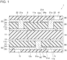
FIG. 1 is a sectional view of a printed wiring board. -
FIG. 2 is an enlarged view of a region II inFIG. 1 . -
FIG. 3 is an enlarged sectional view of a boundary between an outer circumference of a via conductor and an inner circumference of a hole. -
FIG. 4 is an enlarged sectional view of another boundary between the outer circumference of the via conductor and the inner circumference of the hole. -
FIG. 5 is an enlarged sectional view a via conductor according to a variation. -
FIG. 6 is a sectional view of a stacked body in a process of manufacturing a printed wiring board. -
FIG. 7 is a sectional view of the stacked body in a process subsequent to the process inFIG. 6 . -
FIG. 8 is a sectional view of the stacked body in a process subsequent to the process inFIG. 7 . -
FIG. 9 is a sectional view of the stacked body in a process subsequent to the process inFIG. 8 . -
FIG. 10 is a sectional view of the stacked body in a process subsequent to the process inFIG. 9 . -
FIG. 11 is a sectional view of the stacked body in a process subsequent to the process inFIG. 10 . -
FIG. 12 is a sectional view of the stacked body in a process subsequent to the process inFIG. 11 . -
FIG. 13 is a sectional view of the stacked body in a process subsequent to the process inFIG. 12 . - An embodiment will be described hereinafter with reference to the drawings. The drawings to be referred to hereinafter illustrate only simplified principal members necessary for description of the embodiment for convenience of the description. Accordingly, the present disclosure provides a printed
wiring board 1 that may include any appropriate constituent member not illustrated in the drawings. Furthermore, members illustrated in the drawings do not accurately indicate sizes, size ratios, or the like of actual constituent members. - Description is made to the printed
wiring board 1 with reference toFIG. 1 . - The printed
wiring board 1 is a multilayer substrate. The printedwiring board 1 includes acore substrate 10 and afirst buildup layer 20. As illustrated inFIG. 1 , the printedwiring board 1 includes a firstsolder resist layer 40, asecond buildup layer 50, and a secondsolder resist layer 70 as necessary. The secondsolder resist layer 70, thesecond buildup layer 50, thecore substrate 10, thefirst buildup layer 20, and the firstsolder resist layer 40 may be stacked in the mentioned order. - The
core substrate 10 includes abase 11 andconductor layers - The
base 11 is formed into a flat plate shape. Thebase 11 includes afirst surface 11a and asecond surface 11b opposite to thefirst surface 11a. Thefirst surface 11a and thesecond surface 11b are directed in opposite directions. Thebase 11 has a thickness from thefirst surface 11a to thesecond surface 11b. A direction from thefirst surface 11a to thesecond surface 11b and an opposite direction thereof correspond to a thickness direction. - The
base 11 is made of an insulating material. Examples of such an insulating material include organic resins such as epoxy resin, bismaleimide triazine resin, polyimide resin, polyphenylene ether (PPE) resin, polyphenylene oxide (PPO) resin, cyanate ester resin, and a liquid crystal polymer. The insulating material may include two or more of these organic resins mixed together. One, or two or more of these organic resins may be blended with a reinforcer. Examples of the reinforcer include fabric materials such as glass fiber, glass nonwoven fabric, aramid fiber, aramid nonwoven fabric, polyester fiber, and polyester nonwoven fabric. One, or two or more of these organic resins may contain an inorganic filler such as barium sulfate, talc, clay, glass, calcium carbonate, or titanium. - The
conductor layer 12 is stacked on thefirst surface 11a of thebase 11. Theconductor layer 13 is stacked on thesecond surface 11b of thebase 11. Theconductor layers conductor layers - The
core substrate 10 may have a multilayer structure. The multilayer structure can have a following exemplary aspect. For example, the multilayer structure includes a plurality of insulating layers, one or a plurality of internal conductor layers, and two surface conductor layers. The insulating layers are stacked in sequence. The internal conductor layer is interposed between the insulating layers. The two surface conductor layers are stacked respectively on two uppermost surfaces of a stacked body including the plurality of insulating layers identically or similarly to the conductor layers 12 and 13 stacked respectively on thesurfaces base 11. The internal conductor layer and the surface conductor layers constitute a wiring pattern. - The
first buildup layer 20 includes an insulatinglayer 21, at least one viaconductor 22, and asurface conductor layer 23. - The insulating
layer 21 is stacked on a surface of thecore substrate 10. That is, the insulatinglayer 21 covers theconductor layer 12 as well as thefirst surface 11a of thebase 11. In other words, thecore substrate 10 includes theconductor layer 12 stacked on the surface in contact with thebuildup layer 20. The insulatinglayer 21 is exemplarily 40 µm to 100 µm in thickness, that is, a thickness from asurface 12d of theconductor layer 12 opposite to asurface 12c of theconductor layer 12 in contact with thefirst surface 11a to asurface 21d of the insulatinglayer 21 on a side far from thecore substrate 10. - The insulating
layer 21 is made of an insulating material. Examples of such an insulating material include organic resins such as epoxy resin, bismaleimide triazine resin, polyimide resin, polyphenylene ether (PPE) resin, polyphenylene oxide (PPO) resin, cyanate ester resin, polytetrafluoroethylene (PTFE) resin, and a liquid crystal polymer. The insulating material may include two or more of these organic resins mixed together. One, or two or more of these organic resins may be blended with a reinforcer. Examples of the reinforcer include fabric materials such as glass fiber, glass nonwoven fabric, aramid fiber, aramid nonwoven fabric, polyester fiber, and polyester nonwoven fabric. One, or two or more of these organic resins may contain an inorganic filler such as barium sulfate, talc, clay, glass, calcium carbonate, or titanium. - The via
conductor 22 penetrates the insulatinglayer 21 in a thickness direction. Specifically, the insulatinglayer 21 includes at least onehole 21a penetrating the insulatinglayer 21 in the thickness direction such that the viaconductor 22 is filled in each of theholes 21a. The viaconductor 22 is made of a conductive metal such as copper. The viaconductor 22 is coupled and electrically connected to theconductor layer 12 of thecore substrate 10. - When a plurality of via
conductors 22 is provided, these viaconductors 22 disposed to have a pitch of 245 µm can still secure sufficient insulation characteristics. - The
buildup layer 20 may optionally include aseed layer 24 interposed between the insulatinglayer 21 and atop layer 25. Theseed layer 24 preferably has conductivity. Theseed layer 24 is preferably a metal film. -
FIG. 2 is an enlarged view of a region II indicated inFIG. 1 . As illustrated inFIG. 2 , theconductor layer 12 includes portion being in contact with the viaconductor 22 and including asurface 12a that may have a concave surface shape. That is, when theconductor layer 12 includes such a concave portion in contact with the viaconductor 22, the concave portion receives a bottom 22a of the viaconductor 22. This configuration increases a contact area between theconductor layer 12 and the viaconductor 22. This can increase bonding force between theconductor layer 12 and the viaconductor 22. The viaconductor 22 includes an end surface adjacent to theconductor layer 12 and preferably having a convex surface shape. The bottom 22a of the viaconductor 22 is thus fitted to thesurface 12a in the concave surface shape. - As illustrated in
FIG. 1 , the viaconductor 22 is macroscopically formed into a columnar shape surrounding a central axis in the thickness direction of the insulatinglayer 21. A columnar shape herein indicates a shape having a constant diameter of the viaconductor 22 in the thickness direction. The viaconductor 22 is in contact with an inner wall surface of thehole 21a entirely in the thickness direction. As illustrated inFIG. 2 , the inner wall surface of thehole 21a microscopically is formed to have unevenness, and the viaconductor 22 is tightly filled in the unevenness on the inner wall surface of thehole 21a entirely in the thickness direction. That is, the viaconductor 22 is formed to have unevenness that is tightly engaged with the unevenness on the inner wall surface of thehole 21a. -
FIGs. 3 and4 are enlarged sectional views of a boundary between the viaconductor 22 and the inner wall surface of thehole 21a.FIG. 4 illustrates a portion located differently from a portion illustrated inFIG. 3 . As illustrated inFIGs. 3 and4 , the unevenness of the viaconductor 22 includes at least oneprotrusion 22b and at least oneprotrusion 22c. Theprotrusions layer 21. In other words, theprotrusions protrusions layer 21. Theprotrusion 22b is directed to be inclined toward thesurface conductor layer 23 in this case. Otherwise, theprotrusion 22b is directed to be inclined toward thetop layer 25. In still other words, theprotrusion 22b is inclined from a side surface of the viaconductor 22 to be directed toward thesurface conductor layer 23 or thetop layer 25. Theprotrusion 22c is directed to be inclined toward thecore substrate 10. In other words, theprotrusion 22c is inclined from the side surface of the viaconductor 22 to be directed toward thecore substrate 10. - As illustrated in
FIG. 1 , thesurface conductor layer 23 is stacked on thesurface 21d of the insulatinglayer 21 on the side far from thecore substrate 10. Thesurface conductor layer 23 constitutes a wiring pattern. Thesurface conductor layer 23 is electrically connected to the viaconductor 22. - The
surface conductor layer 23 may include theseed layer 24 and thetop layer 25. Thetop layer 25 indicates a metal film included in thesurface conductor layer 23 and positioned to allow theseed layer 24 to be interposed between the insulatinglayer 21 and thetop layer 25. Thetop layer 25 corresponds to part of the metal film constituting thesurface conductor layer 23. Theseed layer 24 and thetop layer 25 are disposed to be stacked in the mentioned order on thesurface 21d of the insulatinglayer 21 on the side far from thecore substrate 10. Theseed layer 24 is exemplarily 2 µm or more and 17 µm or less in thickness. Theseed layer 24 and thetop layer 25 constitute a wiring pattern. Theseed layer 24 and thetop layer 25 are made of a conductive metal such as copper. - The
seed layer 24 includes anopening 24a positioned to be overlapped with thehole 21a. Theopening 24a includes an inner edge positioned to be overlapped with an open edge of thehole 21a or positioned outside the open edge of thehole 21a. Theseed layer 24 includes a taperedportion 24b in a region around theopening 24a. The region around theopening 24a includes the inner edge (or an edge) of theopening 24a and expands in a normal direction from the inner edge to have a predetermined width. The taperedportion 24b is gradually decreased in thickness toward the edge of theopening 24a. In other words, theseed layer 24 is preferred to be gradually increased in thickness outward from the edge of theopening 24a in the normal direction. When theseed layer 24 is shaped to be gradually increased in thickness outward from the edge of theopening 24a in the normal direction, the taperedportion 24b of theseed layer 24 is less likely to be detached from the insulatinglayer 21. A plurality of members such as the insulatinglayer 21, the viaconductor 22, and thetop layer 25 is in contact with each other at a site near the taperedportion 24b of theseed layer 24. Stress is likely to be generated at the site where a plurality of members is in contact with each other due to differences in the thermal expansivity and the Young's modulus between the members. In such a case, theseed layer 24, which is shaped to be gradually increased in thickness outward from the edge of theopening 24a in the normal direction, can reduce stress that is likely to be generated around the edge of theopening 24a at an end of the taperedportion 24b. In this case, theseed layer 24 is particularly preferred to be decreased in thickness toward the edge of theopening 24a. Furthermore, the taperedportion 24b includes a surface that is in contact with thetop layer 25 and that preferably has a curved shape to be convex toward thetop layer 25. Thetop layer 25 is provided continuously to the viaconductor 22 through theopening 24a so as to be integral with the viaconductor 22. Thetop layer 25 includes a portion overlapped with the taperedportion 24b and gradually decreased in thickness toward the edge of theopening 24a. The taperedportion 24b at the edge of theopening 24a has an angle θ that exemplarily exceeds 45 degrees and that is more specifically preferred to be 50 degrees or more and 80 degrees or less. - The
surface conductor layer 23 includes a portion overlapped with the viaconductor 22 and functioning as a land having a diameter larger than a line width of the wiring pattern. The diameter of the land is preferably 200 µm or more and 250 µm or less. - As described above, the printed
wiring board 1 may include thesecond buildup layer 50. Thesecond buildup layer 50 is positioned on a surface of thecore substrate 10 opposite to the surface provided with thefirst buildup layer 20. Thecore substrate 10 may include theconductor layer 13 provided on the surface in contact with thesecond buildup layer 50. Thesecond buildup layer 50 includes an insulatinglayer 51, at least one viaconductor 52, and asurface conductor layer 53. Thesecond buildup layer 50 is provided identically or similarly to thefirst buildup layer 20. The insulatinglayer 51 of thesecond buildup layer 50 corresponds to the insulatinglayer 21 of thefirst buildup layer 20, the viaconductor 52 of thesecond buildup layer 50 corresponds to the viaconductor 22 of thefirst buildup layer 20, and thesurface conductor layer 53 of thesecond buildup layer 50 corresponds to thesurface conductor layer 23 of thefirst buildup layer 20. The insulatinglayer 51 includes ahole 51a corresponding to thehole 21a of the insulatinglayer 21, thesurface conductor layer 53 includes aseed layer 54 corresponding to theseed layer 24 of thesurface conductor layer 23, thesurface conductor layer 53 includes atop layer 55 corresponding to thetop layer 25 of thesurface conductor layer 23, and theseed layer 54 includes anopening 54a corresponding to theopening 24a of theseed layer 24. Identically or similarly to theseed layer 24 including the tapered portion surrounding theopening 24a, theseed layer 54 includes a tapered portion surrounding theopening 54a and gradually decreased in thickness toward an edge of the opening. - The solder resist
layers first buildup layer 20, thecore substrate 10, and thesecond buildup layer 50. That is, the first solder resistlayer 40 covers thesurface conductor layer 23 as well as thesurface 21d of the insulatinglayer 21 on the side far from thecore substrate 10. The second solder resistlayer 70 covers thesurface conductor layer 53 as well as asurface 51d of the insulatinglayer 51 on a side far from thecore substrate 10. - The first solder resist
layer 40 includes at least oneopening 41. Part of thesurface conductor layer 23 is overlapped with theopening 41, and thesurface conductor layer 23 includes a portion positioned inside theopening 41 and functioning as a terminal. Identically or similarly to the first solder resistlayer 40, the second solder resistlayer 70 includes at least oneopening 71. Part of thesurface conductor layer 53 is overlapped with theopening 71, and thesurface conductor layer 53 includes a portion positioned inside theopening 71 and functioning as a terminal. -
- (1)
FIG. 1 exemplarily illustrates a configuration including the singlefirst buildup layer 20. In contrast, a plurality of first buildup layers 20 may be stacked between thecore substrate 10 and the first solder resistlayer 40. Identically or similarly, a plurality of second buildup layers 50 may be stacked between thecore substrate 10 and the second solder resistlayer 70.
When thecore substrate 10 is provided directly thereon with n layers of first buildup layers 20, the viaconductor 22 in each of the second to n-th layers of the first buildup layers 20 is electrically connected to thesurface conductor layer 23 in thefirst buildup layer 20 disposed immediately therebelow. The same or a similar applies to the viaconductor 52 in each of n layers of second buildup layers 50. - (2) In exemplary illustration in
FIG. 2 , the viaconductor 22 and thehole 21a each have a constant diameter in the thickness direction. As illustrated inFIG. 5 , thehole 21a may alternatively include a portion that is close to theconductor layer 12 and that is tapered by being gradually decreased in diameter from theopening 24a toward theconductor layer 12. In this case, the viaconductor 22 accordingly includes a portion that is close to theconductor layer 12 and that is gradually decreased in diameter from theopening 24a toward theconductor layer 12, and theportion 21e is tapered. -
- (1) Conventionally when a via conductor is gradually decreased in diameter from a solder resist layer toward a core substrate to have a truncated cone shape, the via conductor is likely to be disengaged from an insulating layer. In contrast, the via
conductors conductors layers - (2) The via
conductor 22 having the constant diameter in the thickness direction contributes to improvement in the connection reliability between the viaconductor 22 and theconductor layer 12. The viaconductor 22 and theconductor layer 12 have a coupling area larger than a coupling area between the conventional via conductor and a conductor layer. Accordingly, the viaconductor 22 is less likely to be separated from theconductor layer 12 whereas the conventional via conductor is likely to be separated from the conductor layer. Identically or similarly, the viaconductor 52 has the constant diameter in the thickness direction and is thus less likely to be separated from theconductor layer 13. - (3) A difference in the thermal expansivity between the via
conductor 22 and the insulatinglayer 21 may cause separation of the viaconductor 22 from theconductor layer 12. Even in such a case, the viaconductor 52 has the constant diameter in the thickness direction, and the viaconductor 22 is thus less likely to be separated from theconductor layer 12. - (4) The via
conductor 22 includes the bottom 22a having the convex surface shape, theconductor layer 12 includes thesurface 12a having the concave surface shape, and the bottom 22a of the viaconductor 22 is fitted to thesurface 12a having the concave surface shape. This configuration contributes to improvement in the electrical characteristics between the viaconductor 22 and theconductor layer 12. Specifically, this configuration increases the coupling area between the viaconductor 22 and theconductor layer 12 to stabilize electric resistance, electric conductivity, and the like at around a boundary between the viaconductor 22 and theconductor layer 12. The same or a similar applies to the viaconductor 52 and theconductor layer 13. - (5) An outer circumference of the via
conductor 22 and the inner wall surface of thehole 21a form a boundary surface having unevenness, so that the viaconductor 22 and the insulatinglayer 21 achieve high intimate contact properties and high adhesive properties as well as the viaconductor 22 is less likely to be disengaged from the insulatinglayer 21. The same or a similar applies to the viaconductor 52 and the insulatinglayer 51. - (6) Unevenness on the outer circumference of the via
conductor 22 includes the at least oneprotrusion 22b that is inclined toward thetop layer 25 and that sticks from thehole 21a into the insulatinglayer 21. Theprotrusion 22b anchors the viaconductor 22 to the insulatinglayer 21. Accordingly, the viaconductor 22 is less likely to be disengaged from thehole 21a toward thetop layer 25 as well as is less likely to be separated from theconductor layer 12. The same or a similar applies to the viaconductor 52. - (7) The unevenness on the outer circumference of the via
conductor 22 includes the at least oneprotrusion 22c that is inclined toward thecore substrate 10 and that sticks from thehole 21a into the insulatinglayer 21. Theprotrusion 22c anchors the viaconductor 22 to the insulatinglayer 21. Accordingly, theprotrusion 22c improves anchoring effects in comparison to a configuration including only theprotrusion 22b inclined toward thetop layer 25, and the viaconductor 22 is less likely to be separated from thetop layer 25. The same or a similar applies to the viaconductor 52. - (8) The
seed layer 24 includes the taperedportion 24b surrounding theopening 24a, to increase a contact area between theseed layer 24 and thetop layer 25 around theopening 24a in comparison to a case without the taperedportion 24b. This configuration is less likely to cause detachment of thetop layer 25 from theseed layer 24 in the region around theopening 24a, so that the viaconductor 22 is less likely to be disengaged from the insulatinglayer 21. The same or a similar applies to the viaconductor 52. - Description is made to a method of manufacturing the printed
wiring board 1 with reference toFIGs. 6 to 13 . - Initially prepared is a
stacked body 10A. Thestacked body 10A includes thecore substrate 10 and abuildup precursor layer 20A stacked thereon. As necessary, abuildup precursor layer 50A may be stacked on thecore substrate 10 such that the buildup precursor layers 50A and 20A oppose each other to interpose thecore substrate 10. Thestacked body 10A includes theseed layer 54, the insulatinglayer 51, thecore substrate 10, the insulatinglayer 21, and theseed layer 24, which are disposed in the mentioned order as illustrated inFIG. 6 . Thebuildup precursor layer 20A includes the insulatinglayer 21 and theseed layer 24. Thebuildup precursor layer 50A includes the insulatinglayer 51 and theseed layer 54. The seed layers 24 and 54 have not yet constituted any wiring pattern. The insulatinglayer 21 does not include thehole 21a, and the insulatinglayer 51 does not include thehole 51a. At this stage, the seed layers 24 and 54 are exemplarily 3 µm or more and 18 µm or less in thickness. The insulatinglayer 21 is exemplarily 40 µm to 100 µm in thickness. - The
stacked body 10A is exemplarily prepared as in (1) or (2) described below. - (1) Prepreg, a resin film, or the like is stacked on each surface of the
core substrate 10, and metal foil is further stacked on the prepreg, the resin film, or the like. The metal foil and the prepreg, the resin film, or the like, as well as thecore substrate 10 are then heated and pressurized to allow the prepreg or the resin film to be cured and firmly fixed to thecore substrate 10 and the metal foil, so as to obtain the insulatinglayers - (2) A buildup sheet, which includes a resin film or the like and metal foil preliminarily stacked thereon, is stacked on each surface of the
core substrate 10. The buildup sheet and thecore substrate 10 are then heated and pressurized to allow the resin film or the like to be cured and firmly fixed to thecore substrate 10, so as to obtain the insulatinglayers - Subsequently executed is roughing surfaces of the seed layers 24 and 54. Specifically, the surfaces of the seed layers 24 and 54 are etched. The surfaces of the seed layers 24 and 54 are thus roughened and blackened as well as the seed layers 24 and 54 are thinned. After such surface treatment, the seed layers 24 and 54 are exemplarily 2 µm or more and 17 µm or less in thickness.
- Subsequently as illustrated in
FIG. 7 , thestacked body 10A is set in a laser processing machine, and amask 110 is set between a laser oscillator of the laser processing machine and theseed layer 24. Themask 110 includes at least one through-hole 111 having a circular shape and penetrating themask 110. The through-hole 111 has a diameter exemplarily from 2 mm to 3 mm, and more specifically 2.4 mm. - Subsequently as illustrated in
FIG. 8 , the laser processing machine is used to apply alaser beam 150 to theseed layer 24 through the through-hole 111. Theseed layer 24 is provided with theopening 24a where thelaser beam 150 is applied. Theseed layer 24 has already been roughened as described above. Thelaser beam 150 is thus absorbed into theseed layer 24 without being reflected by theseed layer 24. - The laser processing machine has output of the
laser beam 150 exemplarily 10 mJ/shot to 20 mJ/shot, and more specifically 16 mJ/shot. Theopening 24a has a diameter determined in accordance with the diameter of the through-hole 111 and the output of thelaser beam 150. The longer the diameter of the through-hole 111 is, the longer the diameter of theopening 24a is. The higher the output of thelaser beam 150 is, the longer the diameter of theopening 24a is. When the diameter of the through-hole 111 is exemplarily 2.4 mm and the output of thelaser beam 150 is exemplarily 16 mJ/shot, theopening 24a is formed to have 100 µm in diameter. The output of thelaser beam 150 is also called power. - Application of the
laser beam 150 is stopped when thelaser beam 150 reaches a surface of the insulatinglayer 21. - In order to form a plurality of via
conductors 22, a plurality ofopenings 24a is formed in theseed layer 24 by changing the application location of thelaser beam 150. - Subsequently as illustrated in
FIG. 9 , themask 110 is replaced with amask 120 to be set. Themask 120 includes at least one through-hole 121 having a circular shape and penetrating themask 120. The through-hole 121 is shorter in diameter than the through-hole 111 in themask 110. The diameter of the through-hole 121 is exemplarily 1/3 or more and 1/2 or less the diameter of the through-hole 111, and more specifically 1.1 mm. - Subsequently as illustrated in
FIG. 10 , the laser processing machine is used to apply alaser beam 160 to the insulatinglayer 21 through the through-hole 121 and theopening 24a. The insulatinglayer 21 is thus provided with thecircular hole 21a where thelaser beam 160 is applied. Output of thelaser beam 160 is exemplarily 1/15 or more and 1/8 or less the output of thelaser beam 150 for formation of theopening 24a, and more specifically 1.8 mJ/shot. Thehole 21a thus formed is shorter in diameter than theopening 24a. The diameter of thehole 21a is determined in accordance with the diameter of the through-hole 121 and the output of thelaser beam 160. The longer the diameter of the through-hole 121 is, the longer the diameter of thehole 21a is. The higher the output of thelaser beam 160 is, the longer the diameter of thehole 21a is. When theopening 24a is exemplarily formed under the above preferred conditions, the diameter of the through-hole 121 is 1.1 mm, and the output of thelaser beam 160 is exemplarily 1.8 mJ/shot, thehole 21a is formed to have 80 µm in diameter. - Application of the
laser beam 160 is stopped when thelaser beam 160 reaches a surface of theconductor layer 12. Thelaser beam 160 is incident on the surface of theconductor layer 12 for a short period immediately before application of thelaser beam 160 is stopped. The surface of theconductor layer 12 is thus formed into the concave surface shape by thelaser beam 160. - In the above process of sequentially applying the
laser beams seed layer 24 and the insulatinglayer 21, thelaser beam 150 is incident on the region around theopening 24a to form the taperedportion 24b in the region around theopening 24a. - In order to form a plurality of via
conductors 22, a plurality ofholes 21a is formed in the insulatinglayer 21 by changing the application location of thelaser beam 160. - Identically or similarly to the
opening 24a formed in theseed layer 24, theopening 54a is then formed in theseed layer 54. Identically or similarly to thehole 21a formed in the insulatinglayer 21, thehole 51a is subsequently formed in the insulatinglayer 51. - Any smear in the
holes FIG. 11 , such desmearing treatment increases the diameter of thehole 21a to be equal to the diameter of theopening 24a as well as increases the diameter of thehole 51a to be equal to the diameter of theopening 54a. - Plating treatment is subsequently applied to the
stacked body 10A provided with theopenings holes conductors layers stacked body 10A as illustrated inFIG. 12 . - As illustrated in
FIG. 13 , the metal platedlayers - Specifically, resist is initially stacked on each of the metal plated
layers layers layers layer 25A still remaining corresponds to thetop layer 25 constituting the wiring pattern, and the metal platedlayer 55A still remaining corresponds to thetop layer 55 constituting the wiring pattern. - Subsequently, the first solder resist
layer 40 is stacked on the insulatinglayer 21 and thetop layer 25, and the second solder resistlayer 70 is stacked on the insulatinglayer 51 and thetop layer 55. - The printed
wiring board 1 is completed through the above processes. -
- (1) As described above, the wiring pattern on the seed layers 24 and 54 and the
top layers 25 and 5 are formed through a subtractive process. The wiring pattern may alternatively be formed through a modified semi additive process (MSAP). - (2) When there are provided a plurality of first buildup layers 20 and a plurality of second buildup layers 50, an additional insulating
layer 21 and anadditional seed layer 24 are formed on thefirst buildup layer 20 already provided and an additional insulatinglayer 51 and anadditional seed layer 54 are formed on thesecond buildup layer 50 already provided after the process of [2-8]. The processes of [2-4] to [2-8] are then applied to the additional insulatinglayers -
- (1) The through-
hole 121 allowing passage of thelaser beam 160 is shorter in diameter than the through-hole 111. Thehole 21a formed by thelaser beam 160 is thus shorter in diameter than theopening 24a formed by thelaser beam 150. Thehole 21a having been formed includes an inner wall that may be increased in diameter through the desmearing treatment, and thehole 21a and theopening 24a are thus highly possibly approximated or equalized in diameter. In this case, the output of thelaser beam 160 is preferably set to 1/5 to 1/100 of the output of thelaser beam 150. Theseed layer 24 can then come into a state not bulging inward from the edge of thehole 21a. This promotes circulation of a plating solution in thehole 21a. A plated metal preferably grows in thehole 21a and the viaconductor 22 is preferably formed. That is, the viaconductor 22 is less likely to include any void, defect, or the like. The same or a similar applies to the viaconductor 52. The viaconductors hole 21a, and are likely to be buried in the unevenness on the inner wall of thehole 21a. Furthermore, the metal crystals are likely to constitute a crystalline structure including a regulated kink structure with a fewer defects from around the inner wall of thehole 21a to central axes of the viaconductors - (2) Under the above output conditions of the
laser beam 160, thehole 21a is less likely to be increased in diameter by thelaser beam 160 while thelaser beam 160 is being applied to extend thehole 21a toward theconductor layer 12. Accordingly, thehole 21a has an opening size at a site distant from theseed layer 24 substantially equal to an opening size at a site close to theseed layer 24. Thehole 21a is formed to have a constant diameter in the thickness direction even after the desmearing treatment, and the viaconductor 22 is formed to have a constant diameter in the thickness direction. The viaconductor 22 is thus less likely to be disengaged from the insulatinglayer 21 as well as can have a larger contact area with theconductor layer 12 in comparison to a conductor filled in a hole having a tapered shape. The same or a similar applies to the viaconductor 52. - (3) A plated material is typically less likely to adhere to a liquid crystal polymer and a polytetrafluoroethylene resin. Even when the insulating
layer 21 is made of the liquid crystal polymer or the polytetrafluoroethylene resin, the above manufacturing method achieves the viaconductor 22 that is less likely to be disengaged from the insulatinglayer 21. - (4) The diameter of the through-
hole 121 allowing passage of thelaser beam 160 is 1/3 or more and 1/2 or less the diameter of the through-hole 111 allowing passage of thelaser beam 150. The output of thelaser beam 160 is 1/15 or more and 1/8 or less the output of thelaser beam 150 for formation of theopening 24a. Even with the insulatinglayer 21 having 40 µm to 100 µm in thickness, thehole 21a can achieve 5 µm or less as a difference between the opening size at the site close to theseed layer 24 and the opening size at the site distant from theseed layer 24. - (5) The
hole 21a and the viaconductor 22 are formed to have the constant diameters in the thickness direction. The viaconductor 22 can thus have a smaller diameter in the portion close to theseed layer 24 when the opening size of thehole 21a at the site distant from theseed layer 24 is equal to an opening size at a bottom of a tapered hole. The land overlapped with the viaconductor 22 can accordingly be decreased in diameter. When a plurality of viaconductors 22 is provided, the viaconductors 22 can have a shorter pitch therebetween. Even when lands are 225 µm or more and 250 µm or less in diameter and the pitch between the viaconductors 22 is 245 µm, this configuration secures insulation characteristics between the lands and insulation characteristics between the viaconductors 22. - (6) The
opening 24a is formed in theseed layer 24 without through complicated etching treatment. Formation of theopening 24a in theseed layer 24 can thus be simplified in comparison to any other method such as a large window method or a conformal mask method. The large window method includes etching copper foil to form an opening and then applying laser beam machining to a resin layer to form a hole smaller in diameter than the opening. The conformal mask method includes etching copper foil to form an opening and then applying laser beam machining to a resin layer to eventually form a hole larger in diameter than the opening. - (7) Each of the
laser beams - Specific details such as the configurations, structures, positional relationships, and shapes exemplified in the embodiment described above are changeable as appropriate without departing from the purport of the present disclosure. Furthermore, any of the configurations, structures, positional relationships, and shapes exemplified in the above embodiment can be combined as appropriate without departing from the purport of the present disclosure.
- In an embodiment, (1) a printed wiring board includes a core substrate and a buildup layer stacked on the core substrate. The buildup layer includes an insulating layer stacked on the core substrate, a hole penetrating the insulating layer in a thickness direction, and a via conductor filled in the hole. The via conductor has a columnar shape.
- (2) In the printed wiring board according to (1) described above, the hole includes an inner wall surface having unevenness. The via conductor is in contact with the inner wall surface.
- (3) In the printed wiring board according to (1) or (2) described above, the buildup layer includes a surface conductor layer disposed on the insulating layer on a side far from the core substrate. The via conductor includes a side surface directed toward an inner wall surface of the hole. The side surface includes at least one protrusion. The protrusion is inclined to be directed toward the surface conductor layer.
- (4) In the printed wiring board according to (3) described above, the protrusion is inclined to be directed toward the core substrate.
- (5) In the printed wiring board according to (3) or (4) described above, the surface conductor layer includes a seed layer and a top layer. The seed layer is positioned adjacent to the insulating layer, and includes an opening positioned to be overlapped with the via conductor. The opening includes an inner edge positioned to be overlapped with an open edge of the hole or positioned outside the open edge of the hole.
- (6) In the printed wiring board according to (5) described above, the inner edge of the opening defines a region including a tapered portion gradually decreased in thickness toward the open edge.
- (7) In the printed wiring board according to any one of (1) to (6) described above, the core substrate includes a conductor layer on a surface in contact with the buildup layer. The conductor layer includes a portion being in contact with the via conductor and having a concave surface shape.
- In an embodiment, (8) a method of manufacturing a printed wiring board includes: preparing a stacked body including a core substrate and a buildup precursor layer that includes an insulating layer and a seed layer made of a metal in a mentioned order and that is overlapped with the core substrate; disposing, above and adjacent to the seed layer in the stacked body, a first mask including a first through-hole, and applying a first laser beam to the seed layer through the first through-hole to form an opening in the seed layer; disposing, on the seed layer at a position above the first through-hole, a second mask including a second through-hole smaller in diameter than the first through-hole, and applying a second laser beam to the insulating layer through the opening to form a hole in the insulating layer; and applying plating treatment to the insulating layer provided with the hole to grow a plated film on the seed layer and the hole and form a via conductor and a top layer.
- (9) In the manufacturing method according to (8) described above, the second through-hole is 1/3 or more and 1/2 or less the first through-hole in diameter.
- (10) In the manufacturing method according to (8) or (9) described above, output of the second laser beam is 1/15 or more and 1/8 or less output of the first laser beam.
- (11) As to the manufacturing method according to any one of (8) to (10) described above, the method further includes increasing a diameter of the hole so as not to exceed an inner edge of the opening in the seed layer.
-
- 10 core substrate
- 10A stacked body
- 20 first buildup layer
- 20A buildup precursor layer
- 21 insulating layer
- 21a hole
- 22 via conductor
- 22b protrusion
- 22c protrusion
- 24 seed layer
- 24a opening
- 24b tapered portion
- 25 top layer
- 50 second buildup layer
- 50A buildup precursor layer
- 51 insulating layer
- 51a hole
- 52 via conductor
- 54 seed layer
- 54a opening
- 55 top layer
Claims (11)
- A printed wiring board comprising:a core substrate; anda buildup layer stacked on the core substrate; whereinthe buildup layer includesan insulating layer stacked on the core substrate,a hole penetrating the insulating layer in a thickness direction, anda via conductor filled in the hole, andthe via conductor has a columnar shape.
- The printed wiring board according to claim 1, whereinthe hole includes an inner wall surface having unevenness, andthe via conductor is in contact with the inner wall surface.
- The printed wiring board according to claim 1 or 2, whereinthe buildup layer includes a surface conductor layer disposed on the insulating layer on a side far from the core substrate,the via conductor includes a side surface directed toward an inner wall surface of the hole,the side surface includes at least one protrusion, andthe protrusion is inclined to be directed toward the surface conductor layer.
- The printed wiring board according to claim 3, wherein
the protrusion is inclined to be directed toward the core substrate. - The printed wiring board according to claim 3 or 4, whereinthe surface conductor layer includes a seed layer and a top layer,the seed layer is positioned adjacent to the insulating layer, and includes an opening positioned to be overlapped with the via conductor, andthe opening includes an inner edge positioned to be overlapped with an open edge of the hole or positioned outside the open edge of the hole.
- The printed wiring board according to claim 5, wherein the inner edge of the opening defines a region including a tapered portion gradually decreased in thickness toward the open edge.
- The printed wiring board according to any one of claims 1 to 6, wherein the core substrate includes a conductor layer on a surface in contact with the buildup layer, and the conductor layer includes a portion being in contact with the via conductor and having a concave surface shape.
- A method of manufacturing a printed wiring board, the method comprising:preparing a stacked body including a core substrate and a buildup precursor layer that includes an insulating layer and a seed layer made of a metal in a mentioned order and that is overlapped with the core substrate;disposing, above and adjacent to the seed layer in the stacked body, a first mask including a first through-hole, and applying a first laser beam to the seed layer through the first through-hole to form an opening in the seed layer;disposing, on the seed layer at a position above the first through-hole, a second mask including a second through-hole smaller in diameter than the first through-hole, and applying a second laser beam to the insulating layer through the opening to form a hole in the insulating layer; andapplying plating treatment to the insulating layer provided with the hole to grow a plated film on the seed layer and the hole and form a via conductor and a top layer.
- The method of manufacturing the printed wiring board according to claim 8, wherein the second through-hole is 1/3 or more and 1/2 or less the first through-hole in diameter.
- The method of manufacturing the printed wiring board according to claim 8 or 9, wherein output of the second laser beam is 1/15 or more and 1/8 or less output of the first laser beam.
- The method of manufacturing the printed wiring board according to any one of claims 8 to 10, the method further comprising increasing a diameter of the hole that includes an open edge not exceeding an inner edge of the opening in the seed layer.
Applications Claiming Priority (2)
| Application Number | Priority Date | Filing Date | Title |
|---|---|---|---|
| JP2022137463 | 2022-08-31 | ||
| PCT/JP2023/031794 WO2024048713A1 (en) | 2022-08-31 | 2023-08-31 | Printed wiring board and method for manufacturing same |
Publications (1)
| Publication Number | Publication Date |
|---|---|
| EP4583645A1 true EP4583645A1 (en) | 2025-07-09 |
Family
ID=90099810
Family Applications (1)
| Application Number | Title | Priority Date | Filing Date |
|---|---|---|---|
| EP23860475.5A Withdrawn EP4583645A1 (en) | 2022-08-31 | 2023-08-31 | Printed wiring board and method for manufacturing same |
Country Status (4)
| Country | Link |
|---|---|
| EP (1) | EP4583645A1 (en) |
| JP (2) | JP7583228B2 (en) |
| CN (1) | CN119732185A (en) |
| WO (1) | WO2024048713A1 (en) |
Family Cites Families (8)
| Publication number | Priority date | Publication date | Assignee | Title |
|---|---|---|---|---|
| JP3978152B2 (en) * | 2003-05-19 | 2007-09-19 | 住友重機械工業株式会社 | Laser processing method |
| JP4457843B2 (en) * | 2004-10-15 | 2010-04-28 | 住友ベークライト株式会社 | Circuit board manufacturing method |
| KR20090110596A (en) * | 2008-04-18 | 2009-10-22 | 삼성전기주식회사 | Printed Circuit Board and Manufacturing Method |
| WO2010024233A1 (en) * | 2008-08-27 | 2010-03-04 | 日本電気株式会社 | Wiring board capable of containing functional element and method for manufacturing same |
| US8933556B2 (en) * | 2010-01-22 | 2015-01-13 | Ibiden Co., Ltd. | Wiring board |
| JP2014075523A (en) * | 2012-10-05 | 2014-04-24 | Sumitomo Electric Printed Circuit Inc | Printed wiring board and method for manufacturing the same |
| JP6846862B2 (en) | 2015-10-26 | 2021-03-24 | 京セラ株式会社 | Printed wiring board and its manufacturing method |
| JP2021111711A (en) * | 2020-01-10 | 2021-08-02 | 住友電工プリントサーキット株式会社 | Flexible printed wiring board and its manufacturing method |
-
2023
- 2023-08-31 CN CN202380062778.2A patent/CN119732185A/en not_active Withdrawn
- 2023-08-31 EP EP23860475.5A patent/EP4583645A1/en not_active Withdrawn
- 2023-08-31 JP JP2024540014A patent/JP7583228B2/en active Active
- 2023-08-31 WO PCT/JP2023/031794 patent/WO2024048713A1/en not_active Ceased
-
2024
- 2024-10-31 JP JP2024191441A patent/JP2025017372A/en active Pending
Also Published As
| Publication number | Publication date |
|---|---|
| JPWO2024048713A1 (en) | 2024-03-07 |
| CN119732185A (en) | 2025-03-28 |
| JP7583228B2 (en) | 2024-11-13 |
| JP2025017372A (en) | 2025-02-05 |
| WO2024048713A1 (en) | 2024-03-07 |
Similar Documents
| Publication | Publication Date | Title |
|---|---|---|
| US6531661B2 (en) | Multilayer printed circuit board and method of making the same | |
| US8027169B2 (en) | Multilayer printed wiring board for semiconductor devices and method for manufacturing the board | |
| US8580066B2 (en) | Method for manufacturing multilayer wiring substrate | |
| US8093503B2 (en) | Multilayer wiring board | |
| JP4331769B2 (en) | Wiring structure, method for forming the same, and printed wiring board | |
| KR101472633B1 (en) | Hybrid lamination substrate, manufacturing method thereof and package substrate | |
| JP5566720B2 (en) | Multilayer wiring board and manufacturing method thereof | |
| KR101167466B1 (en) | Multi-layer printed circuit board and method of manufacturing the same | |
| US20150027758A1 (en) | Multilayer wiring substrate and manufacturing method therefor | |
| JP2017143254A (en) | Wiring substrate having multilayer embedded capacitor and method of manufacturing the same | |
| JP5284146B2 (en) | Multilayer wiring board and manufacturing method thereof | |
| US20120097319A1 (en) | Method of manufacturing multilayer wiring substrate | |
| KR102561794B1 (en) | Printed circuit board and method of manufacturing the same | |
| US20150313018A1 (en) | Wiring substrate and production method therefor | |
| KR101579019B1 (en) | Multilayer wiring substrate | |
| US20090289030A1 (en) | Method of fabricating printed wiring board | |
| EP4583645A1 (en) | Printed wiring board and method for manufacturing same | |
| JP2017084914A (en) | Printed wiring board and method of manufacturing the same | |
| US20180156841A1 (en) | Structure and Method of Making Circuitized Substrate Assembly | |
| US20250300052A1 (en) | Semiconductor package and fabricating method thereof | |
| JP2009200151A (en) | Circuit board, and manufacturing method thereof | |
| TW202335542A (en) | Printed circuit board and method of manufacturing the same | |
| JP2024117490A (en) | Waveguide substrate and method for manufacturing the same | |
| US20250096105A1 (en) | Package substrate and fabricating method thereof | |
| JP2023178076A (en) | Wiring board, semiconductor device, and wiring board manufacturing method |
Legal Events
| Date | Code | Title | Description |
|---|---|---|---|
| STAA | Information on the status of an ep patent application or granted ep patent |
Free format text: STATUS: THE INTERNATIONAL PUBLICATION HAS BEEN MADE |
|
| PUAI | Public reference made under article 153(3) epc to a published international application that has entered the european phase |
Free format text: ORIGINAL CODE: 0009012 |
|
| STAA | Information on the status of an ep patent application or granted ep patent |
Free format text: STATUS: REQUEST FOR EXAMINATION WAS MADE |
|
| 17P | Request for examination filed |
Effective date: 20250227 |
|
| AK | Designated contracting states |
Kind code of ref document: A1 Designated state(s): AL AT BE BG CH CY CZ DE DK EE ES FI FR GB GR HR HU IE IS IT LI LT LU LV MC ME MK MT NL NO PL PT RO RS SE SI SK SM TR |
|
| DAV | Request for validation of the european patent (deleted) | ||
| DAX | Request for extension of the european patent (deleted) | ||
| STAA | Information on the status of an ep patent application or granted ep patent |
Free format text: STATUS: THE APPLICATION HAS BEEN WITHDRAWN |
|
| 18W | Application withdrawn |
Effective date: 20251229 |