EP4583644A1 - Pattern forming method and baking device - Google Patents
Pattern forming method and baking device Download PDFInfo
- Publication number
- EP4583644A1 EP4583644A1 EP22957331.6A EP22957331A EP4583644A1 EP 4583644 A1 EP4583644 A1 EP 4583644A1 EP 22957331 A EP22957331 A EP 22957331A EP 4583644 A1 EP4583644 A1 EP 4583644A1
- Authority
- EP
- European Patent Office
- Prior art keywords
- pattern
- resin substrate
- fixing plate
- paste
- infrared rays
- Prior art date
- Legal status (The legal status is an assumption and is not a legal conclusion. Google has not performed a legal analysis and makes no representation as to the accuracy of the status listed.)
- Pending
Links
Images
Classifications
-
- H—ELECTRICITY
- H05—ELECTRIC TECHNIQUES NOT OTHERWISE PROVIDED FOR
- H05K—PRINTED CIRCUITS; CASINGS OR CONSTRUCTIONAL DETAILS OF ELECTRIC APPARATUS; MANUFACTURE OF ASSEMBLAGES OF ELECTRICAL COMPONENTS
- H05K3/00—Apparatus or processes for manufacturing printed circuits
- H05K3/10—Apparatus or processes for manufacturing printed circuits in which conductive material is applied to the insulating support in such a manner as to form the desired conductive pattern
- H05K3/12—Apparatus or processes for manufacturing printed circuits in which conductive material is applied to the insulating support in such a manner as to form the desired conductive pattern using thick film techniques, e.g. printing techniques to apply the conductive material or similar techniques for applying conductive paste or ink patterns
- H05K3/1283—After-treatment of the printed patterns, e.g. sintering or curing methods
-
- B—PERFORMING OPERATIONS; TRANSPORTING
- B32—LAYERED PRODUCTS
- B32B—LAYERED PRODUCTS, i.e. PRODUCTS BUILT-UP OF STRATA OF FLAT OR NON-FLAT, e.g. CELLULAR OR HONEYCOMB, FORM
- B32B15/00—Layered products comprising a layer of metal
- B32B15/04—Layered products comprising a layer of metal comprising metal as the main or only constituent of a layer, which is next to another layer of the same or of a different material
- B32B15/08—Layered products comprising a layer of metal comprising metal as the main or only constituent of a layer, which is next to another layer of the same or of a different material of synthetic resin
-
- B—PERFORMING OPERATIONS; TRANSPORTING
- B32—LAYERED PRODUCTS
- B32B—LAYERED PRODUCTS, i.e. PRODUCTS BUILT-UP OF STRATA OF FLAT OR NON-FLAT, e.g. CELLULAR OR HONEYCOMB, FORM
- B32B37/00—Methods or apparatus for laminating, e.g. by curing or by ultrasonic bonding
- B32B37/06—Methods or apparatus for laminating, e.g. by curing or by ultrasonic bonding characterised by the heating method
-
- B—PERFORMING OPERATIONS; TRANSPORTING
- B32—LAYERED PRODUCTS
- B32B—LAYERED PRODUCTS, i.e. PRODUCTS BUILT-UP OF STRATA OF FLAT OR NON-FLAT, e.g. CELLULAR OR HONEYCOMB, FORM
- B32B2457/00—Electrical equipment
- B32B2457/08—PCBs, i.e. printed circuit boards
-
- H—ELECTRICITY
- H05—ELECTRIC TECHNIQUES NOT OTHERWISE PROVIDED FOR
- H05K—PRINTED CIRCUITS; CASINGS OR CONSTRUCTIONAL DETAILS OF ELECTRIC APPARATUS; MANUFACTURE OF ASSEMBLAGES OF ELECTRICAL COMPONENTS
- H05K1/00—Printed circuits
- H05K1/02—Details
- H05K1/0201—Thermal arrangements, e.g. for cooling, heating or preventing overheating
-
- H—ELECTRICITY
- H05—ELECTRIC TECHNIQUES NOT OTHERWISE PROVIDED FOR
- H05K—PRINTED CIRCUITS; CASINGS OR CONSTRUCTIONAL DETAILS OF ELECTRIC APPARATUS; MANUFACTURE OF ASSEMBLAGES OF ELECTRICAL COMPONENTS
- H05K2201/00—Indexing scheme relating to printed circuits covered by H05K1/00
- H05K2201/01—Dielectrics
- H05K2201/0137—Materials
- H05K2201/0145—Polyester, e.g. polyethylene terephthalate [PET], polyethylene naphthalate [PEN]
-
- H—ELECTRICITY
- H05—ELECTRIC TECHNIQUES NOT OTHERWISE PROVIDED FOR
- H05K—PRINTED CIRCUITS; CASINGS OR CONSTRUCTIONAL DETAILS OF ELECTRIC APPARATUS; MANUFACTURE OF ASSEMBLAGES OF ELECTRICAL COMPONENTS
- H05K2203/00—Indexing scheme relating to apparatus or processes for manufacturing printed circuits covered by H05K3/00
- H05K2203/11—Treatments characterised by their effect, e.g. heating, cooling, roughening
- H05K2203/1131—Sintering, i.e. fusing of metal particles to achieve or improve electrical conductivity
-
- H—ELECTRICITY
- H05—ELECTRIC TECHNIQUES NOT OTHERWISE PROVIDED FOR
- H05K—PRINTED CIRCUITS; CASINGS OR CONSTRUCTIONAL DETAILS OF ELECTRIC APPARATUS; MANUFACTURE OF ASSEMBLAGES OF ELECTRICAL COMPONENTS
- H05K3/00—Apparatus or processes for manufacturing printed circuits
- H05K3/10—Apparatus or processes for manufacturing printed circuits in which conductive material is applied to the insulating support in such a manner as to form the desired conductive pattern
- H05K3/20—Apparatus or processes for manufacturing printed circuits in which conductive material is applied to the insulating support in such a manner as to form the desired conductive pattern by affixing prefabricated conductor pattern
- H05K3/207—Apparatus or processes for manufacturing printed circuits in which conductive material is applied to the insulating support in such a manner as to form the desired conductive pattern by affixing prefabricated conductor pattern using a prefabricated paste pattern, ink pattern or powder pattern
Definitions
- the present invention relates to a pattern forming method and a baking apparatus.
- Patent Literature 1 Japanese Patent No. 4956696
- the present invention has been made to solve the above-described problem, and has as its object to execute baking of a conductive paste in a shorter time even if a substrate of a resin having a low heat resistance is used.
- a pattern forming method comprising fixing a resin substrate, on which a paste pattern of a conductive paste is formed, on a fixing plate made of a metal having a thermal capacity per unit volume of 3,000 [kJ/m 3 ⁇ K] or more and a thermal conductivity of 45 [W/m ⁇ K] or more, and baking the paste pattern by irradiating the paste pattern formed on the resin substrate fixed to the fixing plate with near infrared rays, thereby forming a conductive pattern on the resin substrate.
- a peak wavelength range of the near infrared rays is 0.8 to 1.7 ⁇ m.
- the resin substrate is fixed to the fixing plate by a fixing mechanism.
- a baking apparatus comprising a fixing plate made of a metal having a thermal capacity per unit volume of 3,000 [kJ/m 3 ⁇ K] or more and a thermal conductivity of 45 [W/m ⁇ K] or more, and a light source configured to irradiate, with near infrared rays, a paste pattern on a resin substrate which is fixed on the fixing plate and on which the paste pattern of a conductive paste is formed.
- a peak wavelength range of the near infrared rays is 0.8 to 1.7 ⁇ m.
- the apparatus further comprises a fixing mechanism configured to fix the resin substrate to the fixing plate.
- the fixing mechanism is formed by an adhesive layer.
- the conductive paste can be formed by, for example, dispersing fine metal particles of gold, silver, copper, aluminum, nickel, zinc, or tin or conductive fine carbon particles in a resin binder.
- the conductive paste is, for example, a nano silver paste available from Fujikura Kasei.
- the paste pattern 112 can be formed by, for example, a well-known screen printing method.
- the paste pattern 112 can also be formed by an inkjet method.
- the paste pattern 112 can have a thickness of, for example, 2 to 10 ⁇ m. Depending on the resin binder to be used, the thickness of the paste pattern 112 can be 25 ⁇ m.
- the paste pattern 112 formed on the resin substrate 111 fixed to the fixing plate 101 is irradiated with near infrared rays emitted from the light source 102, thereby baking the paste pattern 112 and thus forming a conductive pattern on the resin substrate 111.
- the conductive pattern is, for example, a metal pattern.
- the peak wavelength range of the irradiated near infrared rays is 0.8 to 1.7 ⁇ m.
- the present invention since baking is executed by irradiation of near infrared rays on the fixing plate made of a metal having a thermal capacity per unit volume of 3,000 [kJ/m 3 ⁇ K] or more and a thermal conductivity of 45 [W/m ⁇ K] or more, it is possible to execute baking of a conductive paste in a shorter time even if a substrate of a resin having a low heat resistance is used.
- a synthetic resin such as PET, PEN, or PI
- the synthetic resins other than PI have a low heat resistance, and manufacturing defects (cracks in a printed portion, peeling, holes in a substrate, deformation, and the like) may occur due to the high temperature in baking or drying.
- manufacturing defects cracks in a printed portion, peeling, holes in a substrate, deformation, and the like
- it is possible to suppress thermal deformation in resin substrate manufacturing and efficiently manufacture substrates in a short time.
Landscapes
- Engineering & Computer Science (AREA)
- Manufacturing & Machinery (AREA)
- Microelectronics & Electronic Packaging (AREA)
- Manufacturing Of Printed Wiring (AREA)
Abstract
A resin substrate (111), on which a paste pattern (112) of a metal paste is formed, is fixed on a fixing plate (101) made of a metal having a thermal capacity per unit volume of 3,000 [kJ/m3·K] or more and a thermal conductivity of 45 [W/m·K] or more, and the paste pattern (112) is baked by irradiating the paste pattern (112) formed on the resin substrate (111) fixed to the fixing plate (101) with near infrared rays emitted from a light source (102), thereby forming a conductive pattern on the resin substrate (111). A peak wavelength range of the irradiated near infrared rays is 0.8 to 1.7 µm.
Description
- The present invention relates to a pattern forming method and a baking apparatus.
- In the field of printed electronics such as a printed wiring board, formation of wiring for a resin substrate has been studied extensively. For example, there has been developed a technique of forming a wiring pattern by screen printing or the like. When manufacturing a wiring board of this type, steps such as pattern formation and heating (baking) are performed. Heating of this type is generally mainly performed by lamp annealing using infrared rays (see patent literature 1).
- Patent Literature 1:
Japanese Patent No. 4956696 - Many printed wiring boards using flexible substrates have been used at present. As the material of a flexible substrate of this type, a resin such as polyethylene terephthalate (PET) or polyethylene naphthalate (PEN) is used. Since the material of this type has low heat resistance, the irradiation intensity cannot be made high in conventional heating using infrared irradiation. If baking is executed using a high irradiation intensity, the resin substrate is deformed, and a formed pattern peels off. For this reason, in the conventional technique, since processing is performed using a low irradiation intensity, the step of baking takes long time.
- The present invention has been made to solve the above-described problem, and has as its object to execute baking of a conductive paste in a shorter time even if a substrate of a resin having a low heat resistance is used.
- According to the present invention, there is provided a pattern forming method comprising fixing a resin substrate, on which a paste pattern of a conductive paste is formed, on a fixing plate made of a metal having a thermal capacity per unit volume of 3,000 [kJ/m3·K] or more and a thermal conductivity of 45 [W/m·K] or more, and baking the paste pattern by irradiating the paste pattern formed on the resin substrate fixed to the fixing plate with near infrared rays, thereby forming a conductive pattern on the resin substrate.
- In a configuration example of the pattern forming method, a peak wavelength range of the near infrared rays is 0.8 to 1.7 µm.
- In a configuration example of the pattern forming method, the resin substrate is fixed to the fixing plate by a fixing mechanism.
- In a configuration example of the pattern forming method, the fixing mechanism is an adhesive layer that fixes the resin substrate to the fixing plate.
- According to the present invention, there is provided a baking apparatus comprising a fixing plate made of a metal having a thermal capacity per unit volume of 3,000 [kJ/m3·K] or more and a thermal conductivity of 45 [W/m·K] or more, and a light source configured to irradiate, with near infrared rays, a paste pattern on a resin substrate which is fixed on the fixing plate and on which the paste pattern of a conductive paste is formed.
- In a configuration example of the baking apparatus, a peak wavelength range of the near infrared rays is 0.8 to 1.7 µm.
- In a configuration example of the baking apparatus, the apparatus further comprises a fixing mechanism configured to fix the resin substrate to the fixing plate.
- In a configuration example of the baking apparatus, the fixing mechanism is formed by an adhesive layer.
- As described above, according to the present invention, since baking is executed by irradiation of near infrared rays on a fixing plate made of a metal which has a thermal capacity per unit volume of 3,000 [kJ/m3·K] or more and a thermal conductivity of 45 [W/m·K] or more, baking of a conductive paste can be executed in a shorter time even if a substrate of a rein having a low heat resistance is used.
-
-
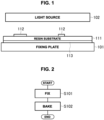
Fig. 1 is a view showing the configuration of a baking apparatus according to the embodiment of the present invention; and -
Fig. 2 is a flowchart for explaining a pattern forming method according to the embodiment of the present invention. - A baking apparatus according to the embodiment of the present invention will now be described with reference to
Fig. 1 . The baking apparatus includes afixing plate 101 and alight source 102. - The
fixing plate 101 is made of a metal having a thermal capacity per unit volume of 3,000 [kJ/m3·K] or more and a thermal conductivity of 45 [W/m·K] or more. The thermal capacity per unit volume [kJ/m3·K] can be obtained by specific heat [kJ/kg·K] × density [kg/m3], which are unique physical property values of an object. Thefixing plate 101 can have a plate thickness of, for example, 0.3 mm or more. Thefixing plate 101 can be made of, for example, copper. Thefixing plate 101 can also be made of red brass whose copper composition is 84% to 96%. Thefixing plate 101 can also be made of brass whose copper composition is 59 to 71.5%. Thefixing plate 101 can also be made of aluminum bronze. Thefixing plate 101 can also be made of tungsten steel. Thefixing plate 101 can also be made of a rolled steel plate. - The
light source 102 irradiates, with near infrared rays, apaste pattern 112 on aresin substrate 111 which is fixed on thefixing plate 101 and on which thepaste pattern 112 of a conductive paste is formed. The peak wavelength range of the near infrared rays is 0.8 to 1.7 µm. Thelight source 102 is instructed on thefixing plate 101 by a support portion (not shown). Thelight source 102 can be arranged at a point apart by about 100 mm from the surface of theresin substrate 111. Thelight source 102 can be formed by, for example, a plurality of near infrared lamps. Thelight source 102 can use, for example, NIR series available from Adphos. - The baking apparatus can also include a
fixing mechanism 113 that fixes theresin substrate 111 to thefixing plate 101. Thefixing mechanism 113 can be formed by, for example, an adhesive layer made of a substance having adhesive properties. Thefixing mechanism 113 may be formed by, for example, an adhesive layer formed by applying a gelatinous adhesive substance or a sheet of elastomer having adhesive properties. - A pattern forming method according to the embodiment of the present invention will be described next with reference to
Fig. 2 . A pattern forming method using the above-described baking apparatus will be described below. - First, in first step S101, the
resin substrate 111 on which thepaste pattern 112 of a conductive paste is formed is fixed on thefixing plate 101 made of a metal having a thermal capacity per unit volume of 3,000 [kJ/m3·K] or more and a thermal conductivity of 45 [W/m·K] or more. Theresin substrate 111 can be fixed to the fixingplate 101 by thefixing mechanism 113. Thefixing mechanism 113 can be an adhesive layer that fixes theresin substrate 111 to the fixingplate 101. - The
resin substrate 111 is made of, for example, a resin such as polyethylene terephthalate, polycarbonate, polypropylene, polyethylene naphthalate, or polyimide (PI). Theresin substrate 111 has a sheet shape having a thickness of, for example, 30 µm to 10 mm. - The conductive paste can be formed by, for example, dispersing fine metal particles of gold, silver, copper, aluminum, nickel, zinc, or tin or conductive fine carbon particles in a resin binder. The conductive paste is, for example, a nano silver paste available from Fujikura Kasei. The
paste pattern 112 can be formed by, for example, a well-known screen printing method. Thepaste pattern 112 can also be formed by an inkjet method. Thepaste pattern 112 can have a thickness of, for example, 2 to 10 µm. Depending on the resin binder to be used, the thickness of thepaste pattern 112 can be 25 µm. - Next, in second step S102, the
paste pattern 112 formed on theresin substrate 111 fixed to the fixingplate 101 is irradiated with near infrared rays emitted from thelight source 102, thereby baking thepaste pattern 112 and thus forming a conductive pattern on theresin substrate 111. The conductive pattern is, for example, a metal pattern. The peak wavelength range of the irradiated near infrared rays is 0.8 to 1.7 µm. - In the
paste pattern 112 irradiated with the near infrared rays (peak wavelength range: 0.8 to 1.7 µm), the contained fine metal particles absorb the irradiated near infrared rays and generate heat. On the other hand, theresin substrate 111 does not absorb the irradiated near infrared rays very well, so it does not generate much heat. For this reason, thepaste pattern 112 is selectively heated by irradiation of the near infrared rays. It is therefore possible to, in a state in which a rise of the temperature of theresin substrate 111 is suppressed, make the irradiation intensity of near infrared rays high and selectively heat thepaste pattern 112 to a high temperature. - On the other hand, since the
paste pattern 112 is heated, theresin substrate 111 at the point where thepaste pattern 112 is formed is heated. The heat of theresin substrate 111 is conducted to the fixingplate 101 and diffused. As a result, the rise of heat is suppressed even in theresin substrate 111 at the point where thepaste pattern 112 is formed. - As a result, according to the embodiment, baking of the
paste pattern 112 can more quickly be executed in a short time in a state in which an occurrence of damages to theresin substrate 111 is prevented. For example, baking of thepaste pattern 112 can be executed with a processing time of 30 sec to 1 min. - Table 1 shows the result of an experiment. In the experiment, a predetermined pattern of a conductive paste (nano silver paste available from Fujikura Kasei) was formed on each of resin substrates (sheets) made of materials shown in Table 1, and heating (lamp annealing) was executed for 1 min using each lamp.
- As for a light source "near infrared rays", three near infrared lamps with a peak wavelength of 0.8 to 1.7 µm were used, and conditions of a total output of 13 kw and an energy density of 380 kw/m2 were set. As for a light source "Xe lamp", an Xe lamp with a peak wavelength of 0.4 to 0.6 µm was used. As for a light source "far infrared rays", one far infrared lamp with a peak wavelength of 3 to 4 µm was used, the total output was set to 1.25 kw, and the energy density was set to 40 kw/m2.
- Also, a wiring pattern having a pattern size of "30 µm or less" and a line width of 30 µm or less was formed, a wiring pattern having a pattern size of "1,000 µm" and a line width of 1,000 µm or less was formed, and a square pattern having a pattern size of "10 mm" and a one-side length of 10 mm was formed. The thicknesses of the patterns were 2 to 10 µm.
- Under the above-described conditions, conduction of each pattern was confirmed in a processing time of 1 min or less, and if deformation of the resin substrate (sheet) was not observed, the determination result of the sample was "○". If the above-described conditions were not satisfied, the determination was result was "×". The conduction was determined based on a resistance value for 90% or more of baking using a hot air drying furnace.
[Table 1] Light source Substrate condition PET PEN PI materials plate thickness [mm] thermal capacity [kJ /m3·K] thermal conductivity [W/m·K] pattern size pattern size pattern size 30 µm or less 1,000 µm 10 mm 30 µm or less 1,000 µm 10 mm 30 µm or less 1,000 µm 10 mm Near infrared rays sheet glass 3 2092.5 1 × × × × × × ○ ○ ○ touch pitch copper 1,3,5,10 3422.65 391 ○ ○ ○ ○ ○ ○ ○ ○ ○ red brass (Cu94-96) 1,3,5 3340.22 234 ○ ○ ○ ○ ○ ○ ○ ○ ○ red brass (Cu89-91) 1,3,5 3317.6 188 ○ ○ ○ ○ ○ ○ ○ ○ ○ red brass (Cu84-86) 1,3,5 3298.75 159 ○ ○ ○ ○ ○ ○ ○ ○ ○ red brass (Cu78.5-81.5) 1,3,5 3268.59 138 ○ ○ ○ ○ ○ ○ ○ ○ ○ 7-3 brass (Cu68.5-71.5) 1,3,5 3215.81 121 ○ ○ ○ ○ ○ ○ ○ ○ ○ 6-4 brass (Cu59-62) 1,3,5 3163.03 121 ○ ○ ○ ○ ○ ○ ○ ○ ○ aluminum bronze (Cu-Al-Zn) 1,3,5 3135 80 ○ ○ ○ ○ ○ ○ ○ ○ ○ gunmetal (Cu-Sn-Pb-Zn) 1,3,5 3344 159 ○ ○ ○ ○ ○ ○ ○ ○ ○ tungsten steel 1,3,5 3530.24 66 ○ ○ ○ ○ ○ ○ ○ ○ ○ rolled steel for general structure 1,3,5 3713.05 51.6 ○ ○ ○ ○ ○ ○ ○ ○ ○ carbon steel 1,3,5 3841.6 45 ○ ○ ○ ○ ○ ○ ○ ○ ○ pure aluminum 1,3,5 2439 222 × × × × × × ○ ○ ○ aluminum alloy (Mg) 1,3,5 2412 137 × × × × × × ○ ○ ○ stainless steel 1,3,5 3965 16 × × × × × × ○ ○ ○ nickel silver (Cu-Ni-Zn) 1,3,5 3439.62 33 × × × × × × ○ ○ ○ Xe lamp all materials × × × × × × × × × Far infrared rays all materials × × × × × × × × × - As shown in Table 1, in the substrate made of a metal which has a thermal capacity per unit volume of 3,000 [kJ/m3·K] or more and a thermal conductivity of 45 [W/m·K] or more, the determination result is "○".
- As described above, according to the present invention, since baking is executed by irradiation of near infrared rays on the fixing plate made of a metal having a thermal capacity per unit volume of 3,000 [kJ/m3·K] or more and a thermal conductivity of 45 [W/m·K] or more, it is possible to execute baking of a conductive paste in a shorter time even if a substrate of a resin having a low heat resistance is used.
- For example, formation of a wiring pattern (conductive pattern) on a printed board or the like is executed by screen printing, and the time needed to form a wiring pattern of one layer is about 1 min. To the contrary, a baking/drying step that is generally performed at present to bake a wiring pattern to form wires takes a time of several ten min to 1 hr or more, and the challenge is how to shorten the time required for the baking/drying step.
- In addition, as a new material of a flexible substrate, a synthetic resin such as PET, PEN, or PI is used. The synthetic resins other than PI have a low heat resistance, and manufacturing defects (cracks in a printed portion, peeling, holes in a substrate, deformation, and the like) may occur due to the high temperature in baking or drying. However, according to the present invention, it is possible to suppress thermal deformation in resin substrate manufacturing and efficiently manufacture substrates in a short time.
- Note that the present invention is not limited the above-described embodiments, and it is obvious that many modifications and combinations can be done by any person ordinarily skilled in the art without departing from the technical scope of the present invention.
- 101...fixing plate, 102...light source, 111...resin substrate, 112...paste pattern, 113...fixing mechanism
Claims (8)
- A pattern forming method comprising:fixing a resin substrate, on which a paste pattern of a conductive paste is formed, on a fixing plate made of a metal having a thermal capacity per unit volume of 3,000 [kJ/m3·K] or more and a thermal conductivity of 45 [W/m·K] or more; andbaking the paste pattern by irradiating the paste pattern formed on the resin substrate fixed to the fixing plate with near infrared rays, thereby forming a conductive pattern on the resin substrate.
- The pattern forming method according to claim 1, wherein
a peak wavelength range of the near infrared rays is 0.8 to 1.7 µm. - The pattern forming method according to claim 1 or 2, wherein
the resin substrate is fixed to the fixing plate by a fixing mechanism. - The pattern forming method according to claim 3, wherein
the fixing mechanism is an adhesive layer that fixes the resin substrate to the fixing plate. - A baking apparatus comprising:a fixing plate made of a metal having a thermal capacity per unit volume of 3,000 [kJ/m3·K] or more and a thermal conductivity of 45 [W/m·K] or more; anda light source configured to irradiate, with near infrared rays, a paste pattern on a resin substrate which is fixed on the fixing plate and on which the paste pattern of a conductive paste is formed.
- The baking apparatus according to claim 5, wherein
a peak wavelength range of the near infrared rays is 0.8 to 1.7 µm. - The baking apparatus according to claim 5 or 6, further comprising
a fixing mechanism configured to fix the resin substrate to the fixing plate. - The baking apparatus according to claim 7, wherein
the fixing mechanism is formed by an adhesive layer.
Applications Claiming Priority (1)
| Application Number | Priority Date | Filing Date | Title |
|---|---|---|---|
| PCT/JP2022/032513 WO2024047728A1 (en) | 2022-08-30 | 2022-08-30 | Pattern forming method and baking device |
Publications (1)
| Publication Number | Publication Date |
|---|---|
| EP4583644A1 true EP4583644A1 (en) | 2025-07-09 |
Family
ID=90098918
Family Applications (1)
| Application Number | Title | Priority Date | Filing Date |
|---|---|---|---|
| EP22957331.6A Pending EP4583644A1 (en) | 2022-08-30 | 2022-08-30 | Pattern forming method and baking device |
Country Status (3)
| Country | Link |
|---|---|
| US (1) | US20260025930A1 (en) |
| EP (1) | EP4583644A1 (en) |
| WO (1) | WO2024047728A1 (en) |
Family Cites Families (7)
| Publication number | Priority date | Publication date | Assignee | Title |
|---|---|---|---|---|
| WO2006076603A2 (en) * | 2005-01-14 | 2006-07-20 | Cabot Corporation | Printable electrical conductors |
| JP5721992B2 (en) * | 2009-10-14 | 2015-05-20 | 富士フイルム株式会社 | Colored curable composition, resist solution, ink-jet ink, color filter, method for producing color filter, solid-state imaging device, liquid crystal display, organic EL display, image display device, and dye compound |
| JP4956696B1 (en) | 2012-01-23 | 2012-06-20 | 日本碍子株式会社 | Method for drying coating film formed on the surface of PET film |
| JP6044849B2 (en) * | 2014-03-24 | 2016-12-14 | コニカミノルタ株式会社 | Processing apparatus and particle fixing method |
| JP7229787B2 (en) * | 2019-01-18 | 2023-02-28 | 東洋紡株式会社 | FIXING MEMBER, FLEXIBLE ELECTRONIC DEVICE MANUFACTURING METHOD, LAMINATED BODY, AND PRINTING APPARATUS |
| EP3725853A1 (en) * | 2019-04-19 | 2020-10-21 | Agfa-Gevaert Nv | A method of manufacturing a conductive pattern |
| JP7400423B2 (en) * | 2019-12-10 | 2023-12-19 | セイコーエプソン株式会社 | Inkjet recording method and inkjet recording device |
-
2022
- 2022-08-30 US US19/107,501 patent/US20260025930A1/en active Pending
- 2022-08-30 EP EP22957331.6A patent/EP4583644A1/en active Pending
- 2022-08-30 WO PCT/JP2022/032513 patent/WO2024047728A1/en not_active Ceased
Also Published As
| Publication number | Publication date |
|---|---|
| WO2024047728A1 (en) | 2024-03-07 |
| US20260025930A1 (en) | 2026-01-22 |
Similar Documents
| Publication | Publication Date | Title |
|---|---|---|
| EP1831432B1 (en) | Method for sintering materials | |
| JP6121417B2 (en) | Conductive pattern forming method | |
| US7049176B2 (en) | Method of forming thick-film wiring and method of producing laminated electronic component | |
| JP2009049136A (en) | Wiring board, wiring pattern forming method, and wiring board manufacturing method | |
| CN101243205B (en) | Conductive circuit manufacturing method | |
| DE60021850T2 (en) | CERAMIC HEATING ELEMENT | |
| US20260025930A1 (en) | Pattern forming method and baking device | |
| JP2004253432A (en) | Manufacturing method of printed wiring board | |
| JP7357099B2 (en) | Pattern forming method and baking device | |
| TWI847244B (en) | Pattern forming method and firing device | |
| KR20230135239A (en) | Flexible film heater | |
| KR20250015969A (en) | Method of manufacturing ceramic circuit board using photo sintering, ceramic circuit board, and power module of double-faced cooling having the same | |
| JP2020119915A (en) | Fixing member, method of manufacturing flexible electronic device, laminate and printing apparatus | |
| CN105393650A (en) | Method for manufacturing conductive line and conductive line | |
| JP2025140988A (en) | Method for manufacturing conductive base material, method for manufacturing electronic device, method for manufacturing electromagnetic wave shield film, and method for manufacturing planar heating element | |
| JP2025141157A (en) | Method for manufacturing conductive base material, method for manufacturing electronic device, method for manufacturing electromagnetic wave shielding film, and method for manufacturing planar heating element | |
| JPH03153308A (en) | Manufacture of ceramic complex | |
| JP6269285B2 (en) | Pattern formation method | |
| KR20170137236A (en) | Light sintering device having protecting damage to substrate | |
| US20250056728A1 (en) | Flexible transparent wiring board and method for manufacturing flexible transparent wiring board | |
| EP4590077A1 (en) | Method for producing conductive base material, method for producing electronic device, method for producing electromagnetic shield film, method for producing sheet-like heating element and conductive composition | |
| JP2001313452A (en) | Manufacturing method and apparatus of thick-film conductive circuit board | |
| JPH09130005A (en) | Method for manufacturing hybrid integrated circuit | |
| JP2025141114A (en) | Base material for conductive pattern, electronic device, electromagnetic shield film and planar heating element | |
| JP2025141077A (en) | Method for manufacturing base material including conductive pattern, method for manufacturing electronic device, method for manufacturing electromagnetic wave shield film, method for manufacturing planar heating element, intermediate structure for manufacturing base material including conductive pattern, and base material including conductive pattern |
Legal Events
| Date | Code | Title | Description |
|---|---|---|---|
| STAA | Information on the status of an ep patent application or granted ep patent |
Free format text: STATUS: THE INTERNATIONAL PUBLICATION HAS BEEN MADE |
|
| PUAI | Public reference made under article 153(3) epc to a published international application that has entered the european phase |
Free format text: ORIGINAL CODE: 0009012 |
|
| STAA | Information on the status of an ep patent application or granted ep patent |
Free format text: STATUS: REQUEST FOR EXAMINATION WAS MADE |
|
| 17P | Request for examination filed |
Effective date: 20250318 |
|
| AK | Designated contracting states |
Kind code of ref document: A1 Designated state(s): AL AT BE BG CH CY CZ DE DK EE ES FI FR GB GR HR HU IE IS IT LI LT LU LV MC MK MT NL NO PL PT RO RS SE SI SK SM TR |
|
| DAV | Request for validation of the european patent (deleted) | ||
| DAX | Request for extension of the european patent (deleted) |