EP4583402A2 - Saw resonator mit schwermetallelektroden, zwischen denen gräben im piezoelektrischen material angeordnet sind - Google Patents
Saw resonator mit schwermetallelektroden, zwischen denen gräben im piezoelektrischen material angeordnet sind Download PDFInfo
- Publication number
- EP4583402A2 EP4583402A2 EP24198489.7A EP24198489A EP4583402A2 EP 4583402 A2 EP4583402 A2 EP 4583402A2 EP 24198489 A EP24198489 A EP 24198489A EP 4583402 A2 EP4583402 A2 EP 4583402A2
- Authority
- EP
- European Patent Office
- Prior art keywords
- heavy metal
- electrodes
- piezoelectric
- saw
- saw resonator
- Prior art date
- Legal status (The legal status is an assumption and is not a legal conclusion. Google has not performed a legal analysis and makes no representation as to the accuracy of the status listed.)
- Pending
Links
Images





Classifications
-
- H—ELECTRICITY
- H03—ELECTRONIC CIRCUITRY
- H03H—IMPEDANCE NETWORKS, e.g. RESONANT CIRCUITS; RESONATORS
- H03H3/00—Apparatus or processes specially adapted for the manufacture of impedance networks, resonating circuits, resonators
- H03H3/007—Apparatus or processes specially adapted for the manufacture of impedance networks, resonating circuits, resonators for the manufacture of electromechanical resonators or networks
- H03H3/08—Apparatus or processes specially adapted for the manufacture of impedance networks, resonating circuits, resonators for the manufacture of electromechanical resonators or networks for the manufacture of resonators or networks using surface acoustic waves
- H03H3/10—Apparatus or processes specially adapted for the manufacture of impedance networks, resonating circuits, resonators for the manufacture of electromechanical resonators or networks for the manufacture of resonators or networks using surface acoustic waves for obtaining desired frequency or temperature coefficient
-
- H—ELECTRICITY
- H03—ELECTRONIC CIRCUITRY
- H03H—IMPEDANCE NETWORKS, e.g. RESONANT CIRCUITS; RESONATORS
- H03H9/00—Networks comprising electromechanical or electro-acoustic elements; Electromechanical resonators
- H03H9/02—Details
- H03H9/125—Driving means, e.g. electrodes, coils
- H03H9/13—Driving means, e.g. electrodes, coils for networks consisting of piezoelectric or electrostrictive materials
-
- H—ELECTRICITY
- H03—ELECTRONIC CIRCUITRY
- H03H—IMPEDANCE NETWORKS, e.g. RESONANT CIRCUITS; RESONATORS
- H03H9/00—Networks comprising electromechanical or electro-acoustic elements; Electromechanical resonators
- H03H9/25—Constructional features of resonators using surface acoustic waves
-
- H—ELECTRICITY
- H03—ELECTRONIC CIRCUITRY
- H03H—IMPEDANCE NETWORKS, e.g. RESONANT CIRCUITS; RESONATORS
- H03H3/00—Apparatus or processes specially adapted for the manufacture of impedance networks, resonating circuits, resonators
- H03H3/007—Apparatus or processes specially adapted for the manufacture of impedance networks, resonating circuits, resonators for the manufacture of electromechanical resonators or networks
- H03H3/08—Apparatus or processes specially adapted for the manufacture of impedance networks, resonating circuits, resonators for the manufacture of electromechanical resonators or networks for the manufacture of resonators or networks using surface acoustic waves
-
- H—ELECTRICITY
- H03—ELECTRONIC CIRCUITRY
- H03H—IMPEDANCE NETWORKS, e.g. RESONANT CIRCUITS; RESONATORS
- H03H9/00—Networks comprising electromechanical or electro-acoustic elements; Electromechanical resonators
- H03H9/02—Details
- H03H9/02535—Details of surface acoustic wave devices
- H03H9/02543—Characteristics of substrate, e.g. cutting angles
- H03H9/02574—Characteristics of substrate, e.g. cutting angles of combined substrates, multilayered substrates, piezoelectrical layers on not-piezoelectrical substrate
-
- H—ELECTRICITY
- H03—ELECTRONIC CIRCUITRY
- H03H—IMPEDANCE NETWORKS, e.g. RESONANT CIRCUITS; RESONATORS
- H03H9/00—Networks comprising electromechanical or electro-acoustic elements; Electromechanical resonators
- H03H9/02—Details
- H03H9/02535—Details of surface acoustic wave devices
- H03H9/02614—Treatment of substrates, e.g. curved, spherical, cylindrical substrates ensuring closed round-about circuits for the acoustical waves
- H03H9/02622—Treatment of substrates, e.g. curved, spherical, cylindrical substrates ensuring closed round-about circuits for the acoustical waves of the surface, including back surface
-
- H—ELECTRICITY
- H03—ELECTRONIC CIRCUITRY
- H03H—IMPEDANCE NETWORKS, e.g. RESONANT CIRCUITS; RESONATORS
- H03H9/00—Networks comprising electromechanical or electro-acoustic elements; Electromechanical resonators
- H03H9/02—Details
- H03H9/02535—Details of surface acoustic wave devices
- H03H9/02637—Details concerning reflective or coupling arrays
- H03H9/02653—Grooves or arrays buried in the substrate
- H03H9/02661—Grooves or arrays buried in the substrate being located inside the interdigital transducers
-
- H—ELECTRICITY
- H03—ELECTRONIC CIRCUITRY
- H03H—IMPEDANCE NETWORKS, e.g. RESONANT CIRCUITS; RESONATORS
- H03H9/00—Networks comprising electromechanical or electro-acoustic elements; Electromechanical resonators
- H03H9/02—Details
- H03H9/02535—Details of surface acoustic wave devices
- H03H9/02818—Means for compensation or elimination of undesirable effects
-
- H—ELECTRICITY
- H03—ELECTRONIC CIRCUITRY
- H03H—IMPEDANCE NETWORKS, e.g. RESONANT CIRCUITS; RESONATORS
- H03H9/00—Networks comprising electromechanical or electro-acoustic elements; Electromechanical resonators
- H03H9/02—Details
- H03H9/02535—Details of surface acoustic wave devices
- H03H9/02818—Means for compensation or elimination of undesirable effects
- H03H9/02889—Means for compensation or elimination of undesirable effects of influence of mass loading
-
- H—ELECTRICITY
- H03—ELECTRONIC CIRCUITRY
- H03H—IMPEDANCE NETWORKS, e.g. RESONANT CIRCUITS; RESONATORS
- H03H9/00—Networks comprising electromechanical or electro-acoustic elements; Electromechanical resonators
- H03H9/02—Details
- H03H9/125—Driving means, e.g. electrodes, coils
- H03H9/145—Driving means, e.g. electrodes, coils for networks using surface acoustic waves
-
- H—ELECTRICITY
- H03—ELECTRONIC CIRCUITRY
- H03H—IMPEDANCE NETWORKS, e.g. RESONANT CIRCUITS; RESONATORS
- H03H9/00—Networks comprising electromechanical or electro-acoustic elements; Electromechanical resonators
- H03H9/02—Details
- H03H9/125—Driving means, e.g. electrodes, coils
- H03H9/145—Driving means, e.g. electrodes, coils for networks using surface acoustic waves
- H03H9/14538—Formation
- H03H9/14541—Multilayer finger or busbar electrode
-
- H—ELECTRICITY
- H03—ELECTRONIC CIRCUITRY
- H03H—IMPEDANCE NETWORKS, e.g. RESONANT CIRCUITS; RESONATORS
- H03H9/00—Networks comprising electromechanical or electro-acoustic elements; Electromechanical resonators
- H03H9/02—Details
- H03H9/02535—Details of surface acoustic wave devices
- H03H9/02543—Characteristics of substrate, e.g. cutting angles
- H03H9/02559—Characteristics of substrate, e.g. cutting angles of lithium niobate or lithium-tantalate substrates
-
- H—ELECTRICITY
- H03—ELECTRONIC CIRCUITRY
- H03H—IMPEDANCE NETWORKS, e.g. RESONANT CIRCUITS; RESONATORS
- H03H9/00—Networks comprising electromechanical or electro-acoustic elements; Electromechanical resonators
- H03H9/46—Filters
- H03H9/64—Filters using surface acoustic waves
- H03H9/6423—Means for obtaining a particular transfer characteristic
- H03H9/6433—Coupled resonator filters
- H03H9/6483—Ladder SAW filters
Definitions
- acoustic wave (AW) resonators are widespread in communication applications due to several performance advantages, including low insertion loss, high selectivity, and small size. Aspects of acoustic wave (AW) resonators include bulk acoustic wave (BAW) and surface acoustic wave (SAW) resonators. Designing AW filters with low insertion loss, large enough passband width, good out-of-band rejection, and good isolation requires the technology and resonator geometry to be optimized for sufficient coupling, high quality factor, largely suppressing all spurious mode types as well as reducing loss mechanisms in all three dimensions. Following these principles typically enables construction of AW filters with sufficiently high signal quality by minimizing ripples and loss mechanism in the filter response. Unwanted responses can be caused by the same filter or other filters within a multiplexer circuit. Cleaning up resonator responses in a large frequency range is, therefore, an important goal for improvements over existing AW resonator technology.
- BAW bulk acoustic wave
- SAW surface
- a surface acoustic wave (SAW) resonator device includes a first electrode positioned on an upper surface of a piezoelectric film, the first electrode comprising a plurality of layers wherein a layer of the plurality of layers is a first heavy metal layer; and a first piezoelectric trench (PZT) positioned adjacent to the first electrode, the first PZT including a recess in the piezoelectric film.
- SAW surface acoustic wave
- the heavy metal layer of the first electrode is made of platinum. In some aspects, the heavy metal layer of the first electrode is made of tungsten. In some aspects, the heavy metal layer of the first electrode is made of gold. In some aspects, the first electrode further comprises a second heavy metal layer. In some aspects, the first heavy metal layer and the second heavy metal layer are separated by a conductive layer. In some aspects, the first PZT is positioned between the first electrode and a second electrode positioned on the upper surface of the piezoelectric film. In some aspects, the SAW resonator device further includes a second electrode including a second heavy metal layer. In some aspects, the second electrode includes a third heavy metal layer.
- the first PZT is an upper PZT formed within the upper surface of the piezoelectric film. In some aspects, the first PZT is a lower PZT formed within the lower surface of the piezoelectric film. In some aspects, a first trench depth of the first PZT is equal to or less than the thickness of the piezoelectric film. In some aspects, a trench depth equal to the thickness of the piezoelectric film corresponds to a fully-etched PZT. In some aspects, the SAW resonator device further includes a second PZT positioned within the piezoelectric film on a side of the first electrode opposite the first PZT.
- a surface acoustic wave (SAW) resonator device includes a plurality of electrodes positioned on an upper surface of a piezoelectric film of a first thickness, each electrode of the plurality of electrodes comprising at least one heavy metal layer; and a plurality of piezoelectric trenches (PZTs) formed within the piezoelectric film between the plurality of electrodes, wherein the plurality of PZTs correspond to regions of the piezoelectric film of a second thickness less than the first thickness.
- SAW surface acoustic wave
- a method includes receiving a surface acoustic wave (SAW) resonator device, the device comprising: a piezoelectric film; an interdigital transducer including a plurality of interleaved electrodes positioned on the piezoelectric film, each electrode of the plurality of interleaved electrodes comprising a heavy metal layer; and a sacrificial layer positioned on the plurality of interleaved electrodes; and applying an ion beam to the upper surface of the SAW resonator device such that the sacrificial layer is removed and forming piezoelectric trenches (PZTs) between the plurality of interleaved electrodes.
- SAW surface acoustic wave
- the method further includes patterning the plurality of interleaved electrodes on the piezoelectric film; and patterning the sacrificial layer on the plurality of interleaved electrodes.
- the interleaved electrodes and sacrificial material are patterned by sputtering, lithography, and dry etching.
- Example embodiments of the present disclosure relate to SAW resonators with electrodes including heavy metal layers and piezoelectric trenches (PZTs) between the electrodes.
- guided SAW type technologies have high quality factor, high coupling, and low TCF.
- a SAW resonator such as the one shown and described in Fig. 1 may additionally be referred to as an LRT-SAW, multi-layer SAW, thin film SAW, or any other suitable term. Any of these terms may be used in the present disclosure and are not intended to be limiting.
- a key improvement point for this type of technology is to reduce existing loss mechanisms and spurious acoustic modes.
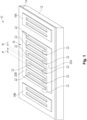
- Fig. 1 is a perspective view of a representative surface acoustic wave (SAW) device, according to aspects of the present disclosure. While this disclosure describes principles of the techniques in the context of a SAW resonator, it should be understood that the technology presented may be applied to any suitable type of acoustic wave (AW) resonator, including SAW resonators and BAW resonators equally. It particularly can be applied to any AW resonator that employs interdigital transducer electrodes, for various orientations of the acoustic wave propagation and the displacements with respect to the arrangement of the electrodes.
- AW acoustic wave
- the SAW device 10 includes a substrate 12, a piezoelectric layer 14 on the substrate 12, an interdigital transducer (IDT) 16 including electrodes 22 on a surface of the piezoelectric layer 14 opposite the substrate 12, a first reflector structure 18A on the surface of the piezoelectric layer 14 adjacent to the interdigital transducer 16, and a second reflector structure 18B on the surface of the piezoelectric layer 14 adjacent to the interdigital transducer 16 opposite the first reflector structure 18A.
- an interdigital transducer may also be referred to as an interdigitated transducer.
- the substrate 12 may be referred to as a carrier substrate and the overall SAW device 10 may be referred to as a guided SAW device.
- the interdigital transducer 16 includes a first electrode 20A and a second electrode 20B, each of which include a number of electrodes 22 that are interleaved with one another as shown.
- the first electrode 20A and the second electrode 20B may also be referred to as comb electrodes.
- a lateral distance between adjacent electrodes 22 of the first electrode 20A and the second electrode 20B defines a pitch P between adjacent electrodes 22.
- the pitch P may at least partially define a resonant frequency of the corresponding electrode(s) 22.
- all electrodes 22 may be configured to correspond to the same resonant frequency. This resonant frequency may be the resonant frequency of the SAW device 10.
- a resonant frequency may be the center frequency or primary frequency of mechanical waves generated in the piezoelectric layer 14 by one or more electrodes 22.
- An electrode width W of the adjacent electrodes 22 together with the pitch P may define a metallization ratio, or duty factor, of electrodes 22.
- the substrate 12 may comprise various materials including glass, sapphire, quartz, diamond, silicon (Si), or gallium arsenide (GaAs) among others, with Si being a common choice.
- the piezoelectric layer 14 may be formed of any suitable piezoelectric material(s). In certain embodiments described herein, the piezoelectric layer 14 is formed of lithium tantalate (LT), or lithium niobate (LiNb03 or LN), but is not limited thereto. In certain embodiments, the piezoelectric layer 14 is thick enough or rigid enough to function as a piezoelectric substrate. Accordingly, the substrate 12 in FIG. 1 may be omitted.
- the interdigital transducer 16, the first reflector structure 18A, and the second reflector structure 18B may comprise one or more electrically conductive materials, including titanium (Ti), aluminum (Al), copper (Cu), and alloys thereof as well as alloys with other suitable materials and can be made of either single or multiple layer arrangements, among others. While not shown to avoid obscuring the drawings, additional dielectric layers or any other layers may be provided over all or a portion of the exposed surface of the piezoelectric layer 14, the interdigital transducer 16, the first reflector structure 18A, and the second reflector structure 18B.
- Such additional passivation layers can form any surface topography, including but not limited to conformal coatings and flat surfaces.
- Such additional dielectric layers may be provided for passivation, for frequency trimming, for temperature compensation purposes and/or improved thermal conductivity, among other reasons.
- Suitable materials for such layers include silicon oxide, silicon nitride, titanium oxide, aluminum oxide and can also include dopants such as fluorine.
- one or more layers may be provided between the substrate 12 and the piezoelectric layer 14 in various embodiments.
- a SAW resonator such as the one shown and described in Fig. 1 may additionally be referred to as a guided SAW, LRT-SAW, multi-layer SAW, thin film SAW, or any other suitable term.
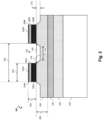
- Fig. 2 is a cross-sectional side view of a SAW resonator 200.
- the SAW resonator 200 comprises various components including a carrier substrate 245, a dielectric layer 240, a dielectric layer 235, a piezoelectric film 230, and two electrodes 222A and 222B.
- the dielectric layer 240 is positioned on top of the carrier substrate 245 and provides electrical insulation between the carrier substrate 245 and the rest of the SAW resonator 200.
- the dielectric layer 240 may additionally provide a velocity contrast to the piezoelectric layer to help with guiding the wave localized mainly in the piezoelectric layer.
- the dielectric layer 240 may additionally help to avoid losses due to overlap with the carrier material as well as reduce TCF.
- the dielectric layer 240 may be made from a variety of materials including silicon dioxide, silicon oxide, silicon nitride, or aluminum oxide, or any other material, depending on the requirements of the specific application.
- a common choice for the piezoelectric material may be lithium tantalate, with an orientation typically between Y+0° and Y+60° and a propagation along the x-axis of the crystal. Orientations close to 42° Y-X LT are a common choice, while orientations close to 30° Y-X LT can in some cases lead to minimized excitation of Rayleigh-type spurious acoustic modes.
- Another common choice for the piezoelectric material may be lithium niobate, with an orientation typically between Y-20° and Y+60° and a propagation along the x-axis of the crystal. Orientations close to 10° Y-X LN and 20° Y-X LN may be implemented, but are not limiting. A large coupling coefficient can be obtained. In these piezoelectric layers, the devices primarily excite waves with shear horizontal displacements, while the techniques disclosed here are not limited to optimization concerning this wave type.
- the electrodes 222A and 222B are positioned on top of the piezoelectric film 230 and excite the piezoelectric film 230.
- the transducers 222A and 222B are transducers within a series of alternating and/or interleaved fingers (see, for example, electrodes 22 of Fig. 1 ). In operation, one of the transducers 222A or 222B may be connected to a positive electrical potential while the other is connected to a negative potential, resulting in the production of acoustic waves in the piezoelectric film 230.
- the transducers 222A and 222B each include a plurality of layers, as illustrated in Fig. 2 .
- the electrode 222A may include a layer 224A, a layer 226A, and a layer 228A.
- the electrode 222A, as well as any other electrodes may alternatively include any suitable number or types of layers in addition to or alternative to the layers shown and described with reference to Fig. 2 .
- the electrode 222B may include a layer 224B, a layer 226B, and a layer 228B.
- the layers 228A and 228B will be described together with reference to the layer 228.
- layers 226A and 226B and layers 224A and 224B will be explained in conjunction.
- the layer 228 may facilitate adhesion to the wafer, to avoid migration of atoms (into the substrate and along the surface) and to lead to suitable crystallinity of the layers above.
- the layer 228 may be a heavy metal.
- the layer 228 may be referred to as a heavy metal layer.
- an electrode that includes at least one heavy metal layer may be referred to as a heavy metal electrode.
- the layer 228 may be constructed of any suitable heavy metal.
- the layer 228 may be constructed of Osmium, Iridium, Platinum, Rhenium, Gold, Tungsten, Tantal, Hafnium, Rhodium, Ruthenium, Thallium, Lead, Silver, Molybdenum, Palladium and alloys containing one or more of the mentioned materials.
- the layer 228 is constructed of a heavy metal, the velocity of the acoustic wave generated by the SAW resonator 200 may be decreased.
- the reflectivity of the SAW resonator 200 may be increased. These effects may be modified by varying the thickness of the layer 228.
- the quality factor of the SAW resonator 200 may begin to decrease introducing insertion loss. This may be a result of increasing overlap of the acoustic wave mode with intrinsically lossy metallic materials.
- the velocity of the acoustic wave of the SAW resonator 200 may be decreased and the reflectivity of the SAW resonator 200 may be increased alternatively by increasing the depth of the piezoelectric trenches (PZTs) 270 positioned between the electrodes 222.
- PZTs piezoelectric trenches
- increasing the depth of the PZTs 270 may decrease wave velocity and increase reflectivity.
- the quality factor of the resonator 200 may begin to decrease.
- PZTs 270 may be introduced and/or deepened to further reduce wave velocity and increase reflectivity without negatively impacting the quality factor of the resonator 200.
- the layer 226 may be constructed of an electrical conductor (e.g., copper or aluminum). The layer 226 may ensure a small resistance and low electric losses in the IDT fingers.
- the layer 224 may provide adhesion of additional metal layers (e.g. underbump metals for routing) and may help to prevent oxidation and degradation of the layers below.
- the electrodes 222 may include additional barrier layers or stacks of layers for the similar purposes including to lower sheet resistance, lower mechanical damping, or increased robustness to withstand environmental conditions such as moisture or excitation under high power.
- the layer 224 may be constructed of any suitable material.
- the layer 224 may be a sacrificial layer, which may be partially or entirely removed during a trim without passivation ("trim without PAS") procedure.
- the SAW resonator 200 also illustrates a piezoelectric trench (PZT) 270.
- the PZT 270 may be formed with a trim without PAS procedure after the SAW resonator 200 is assembled.
- the PZT 270 may be formed in any other way.
- a trim without PAS procedure includes removing material from the SAW resonator 200 with an ion beam.
- the ion beam may be a beam of charged particles, such as ions, that are accelerated and focused to areas of a resonator using lithography techniques. The ion beam can be scanned across the surface of the resonator to selectively remove material.
- the shape of the resonator can be altered. Additionally, a trim without PAS procedure can also be applied to the reflectors 18A and 18B of the SAW resonator 200.
- the reflectors 18A and 18B may also be referred to as gratings.
- the resonator may first be designed with a fundamental resonance frequency that is higher than the desired fundamental resonance frequency.
- a trim without PAS procedure may be performed on the SAW resonator 200.
- the geometry of the SAW resonator 200 shown in Fig. 2 may be a resulting cross-sectional shape of the SAW resonator 200.
- the fundamental resonance frequency may be shifted downward to a desired fundamental resonance frequency.
- the fundamental resonance frequency can be precisely controlled to achieve the desired frequency.
- the electrodes 222 may be of a thickness 250.
- the width of the electrodes 222 may be a width 232 and the electrodes 222 may be spaced according to a pitch 242.
- additional layers be provided over all or a portion of the piezoelectric surface, within the PZT or and/or on top of the electrodes. This may include dielectric layers which may serve for temperature compensation, passivation, frequency trimming or other purposes.
- the performance of the SAW resonator 200 is greatly improved over standard SAW resonators that do not include electrodes with heavy metal layers (i.e., heavy metal electrodes) or PZTs.
- the electrodes 222 of the SAW resonator 200 may include multiple heavy metal layers.
- the electrode 222A shown in Fig. 2 includes a single heavy metal layer 228A, the electrode 222A may alternatively include multiple heavy metal layers.
- multiple heavy metal layers may be separated within the stack by conductive layers similar to the layer 226A.
- each heavy metal layer may individually contribute to slowing of the wave, while the heavy metal layer closest to the piezoelectric surface would contribute more to ensuring high quality factor of the resonator (due to less damping, higher material Q of that layer) as well as contributing more to reliability making it less prone to acousto-migration, while the other heavy metal layers higher in the stack could fulfill other additional purposes, such as contributing partially to improved electrical conductivity.
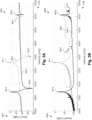
- Fig. 3A is a graphical representation of the absolute value of the admittance of SAW resonators with and without piezoelectric trenches and heavy-metal electrodes, according to aspects of the present disclosure.
- Fig. 3A includes a plot 300A.
- the plot 300A may include an x-axis 310A corresponding to frequency and a y-axis 320A corresponding to admittance.
- the data set 330-1 represents the admittance of a SAW resonator that does not include heavy metal electrodes or PZTs.
- the data set 330-2 represents the frequency response of a SAW resonator that does include both heavy metal electrodes and PZTs (such as the SAW resonator 200 ( Fig.
- Both data sets exhibit a resonance frequency 331 and an anti-resonance frequency 332.
- the resonance frequency 331 represents the frequency at which the SAW resonator has maximum admittance
- the anti-resonance frequency 332 represents the frequency at which the SAW resonator has minimum admittance.
- the resonance frequency 331-2 and the anti-resonance frequency 332-2 are shifted dramatically lower along the frequency spectrum as compared to the resonance frequency 331-1 and the anti-resonance frequency 332-1.
- Fig. 3A additionally shows spurious content 333-1 and 333-2.
- the resonance and anti-resonance frequencies of the data set 330-2 are shifted lower than those of the data set 330-1 by a similar amount.
- the frequency shift may depend on factors such as the type of ion beam used for a trim without PAS procedure, the angle of incidence, the duration of the trim, the type of heavy metal of the heavy metal electrodes, and thickness of the heavy metal layer.
- the spurious content 333-2 is actually shifted upwards in frequency relative to the spurious content 333-1.
- This change in the frequency response, both of the resonance and antiresonance as well as the spurious content can be used to optimize the SAW resonator design and improve its performance.
- the frequency shift can be used to adjust the resonance frequency of the SAW resonator to a desired value. This can be particularly useful in applications such as filters, where a precise frequency response is required.
- the inclusion of a PZT as well as the inclusion of a heavy metal layer within an electrode of a SAW resonator may result in a decrease in the fundamental resonance frequency.
- the SAW resonator may be selected such that, after any necessary trim without PAS procedures, the final resonance frequency corresponds to the desired target resonance frequency.
- the SAW resonator may be designed to include PZTs and heavy metal layers as explained and designed to the desired resonance frequency.
- the data of Figs. 4Aa-4d may be normalized about the fundamental resonance frequency.
- Fig. 4B is a graphical representation of a conductance of SAW resonators with piezoelectric trenches and heavy-metal electrodes normalized to a common resonance frequency, according to aspects of the present disclosure.
- Fig. 4B includes a plot 400B.
- the plot 400B includes a data set 440-1 and a data set 440-2.
- the data set 440-1 may be a data set corresponding to a frequency response of a SAW resonator that does not include heavy metal electrodes or PZTs.
- the data set 440-2 may be a data set corresponding to the SAW resonator that does include both heavy metal electrodes and PZTs (such as the SAW resonator 200 ( Fig. 2 )).
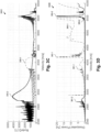
- Fig. 4C is a graphical representation of a quality factor of SAW resonators with piezoelectric trenches and heavy-metal electrodes normalized to a common resonance frequency, according to aspects of the present disclosure.
- Fig. 4C includes a plot 400C.
- the plot 400C includes a data set 450-1 and a data set 450-2.
- the data set 450-1 may be a data set corresponding to a frequency response of a SAW resonator that does not include heavy metal electrodes or PZTs.
- the data set 450-2 may be a data set corresponding to the SAW resonator that does include both heavy metal electrodes and PZTs (such as the SAW resonator 200 ( Fig. 2 )).
- the data sets of the plot 400C are normalized about the resonance frequency for comparison.
- the quality factor of the SAW resonator of the data set 450-2 is greater than the quality factor of the data set 450-1.
- an increase in the quality factor of a SAW resonator may correspond to a reduced loss of the SAW resonator.
- this reduced loss may be a result of acoustic energy being located further away from the metal electrodes. In that regard, the more the trench depth is increased and/or the thicker the heavy metal layer of one or more heavy metal electrodes, the more the quality factor is improved.
- Fig. 4D a graphical representation of dissipated power of SAW resonators with and without piezoelectric trenches and heavy-metal electrodes normalized to a common resonance frequency, according to aspects of the present disclosure.
- the dissipated power may also be referred to as absorbed power.
- Fig. 4D includes a plot 400D.
- the plot 400D includes a data set 460-1 and a data set 460-2.
- the data set 460-1 may be a data set corresponding to a frequency response of a SAW resonator that does not include heavy metal electrodes or PZTs.
- the data set 460-2 may be a data set corresponding to the SAW resonator that does include both heavy metal electrodes and PZTs (such as the SAW resonator 200 ( Fig. 2 )).
- the data sets of the plot 400D are normalized about the resonance frequency for comparison. As shown in Fig. 4D , the dissipated power of the data set 460-2 is significantly improved over the dissipated power of the data set 460-1.
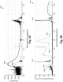
- Fig. 5A is a graphical representation of the absolute value of the admittance of SAW resonators with and without piezoelectric trenches and heavy-metal electrodes normalized to a common resonance frequency and illustrating extended high-frequency range, according to aspects of the present disclosure.
- Fig. 5A includes a plot 500A.
- Plot 500A may be substantially similar to plot 400A of Fig. 4A .
- plot 500A may include more high frequency content of the same data.
- plot 500A may additionally illustrate spurious content 432-2.
- spurious content 432-2 may be shifted dramatically higher in frequency than spurious content 432-1.
- Fig. 5B is a graphical representation of a conductance of SAW resonators with piezoelectric trenches and heavy-metal electrodes normalized to a common resonance frequency and illustrating extended high-frequency range, according to aspects of the present disclosure.
- Fig. 5B includes a plot 500B.
- Plot 500B may be substantially similar to plot 400B of Fig. 4B .
- plot 500B may include more high frequency content of the same data.
- the data set 440-1 includes a peak 442-1, as described with reference to Fig. 4A .
- the data set 440-2 includes a peak 442-2.
- the peak corresponding to the upper stop band edge may be moved higher along the frequency spectrum. The degree to which this shift in the upper stop band edge occurs is shown more clearly by the plot 500B of Fig. 5B as the fundamental frequency has been normalized.
- the peak 442-2 corresponding to a SAW resonator with PZTs and heavy metal layers is significantly higher in frequency than the peak 442-1. This shifting of the upper stop band edge may move spurious content out of the passband of the frequency as well as out of passbands of other filters leading to significantly increased signal quality and performance of multiplexer circuits.
- Fig. 5C is a graphical representation of a quality factor of SAW resonators with piezoelectric trenches and heavy-metal electrodes normalized to a common resonance frequency and illustrating extended high-frequency range, according to aspects of the present disclosure.
- Fig. 5C includes a plot 500C.
- Plot 500C may be substantially similar to plot 400C of Fig. 4C .
- plot 500C may include more high frequency content of the same data.
- the quality factor of the SAW resonator of the data set 450-2 is greater than the quality factor of the data set 450-1.
- Fig. 5D is a graphical representation of dissipated power of SAW resonators with piezoelectric trenches and heavy-metal electrodes normalized to a common resonance frequency and illustrating extended high-frequency range, according to aspects of the present disclosure.
- Fig. 5D includes a plot 500D.
- the plot 500D includes a dataset 560-1 corresponding to a SAW resonator that does not include heavy metal electrodes or PZTs.
- the plot 500D also includes a dataset 560-2 corresponding to a SAW resonator that does include both heavy metal electrodes and PZTs (such as the SAW resonator 200 ( Fig. 2 )).
- Data set 560-1 includes a peak 561-1 and a peak 562-1.
- Data set 560-2 includes a peak 561-2 and a peak 562-2.
- the peak corresponding to the upper stop band edge e.g., peak 562-2
- the peak corresponding to the upper stop band edge may be moved higher along the frequency spectrum.
- Fig. 6 is a graphical representation of a comparison of the performance of SAW ladder filters including series and parallel resonators, based on resonators with and without piezoelectric trenches and heavy-metal electrodes, according to aspects of the present disclosure.
- Fig. 6 includes a plot 600A.
- the plot 600A corresponds to a comparison of a frequency response of a filter, including SAW resonators which do not include PZTs or heavy metal layers with a frequency response of a filter including SAW resonators which include PZTs and heavy metal layers for improved performance.
- the plots include data 6100-1 corresponding to aspects of a filter with SAW resonators without PZTs or heavy metal layers as well as data 6100-2 corresponding to aspects of a filter with SAW resonators with PZTs and heavy metal layers.
- Each of the plots of Fig. 6 also highlight multiple frequency bands for mobile communication.
- frequency bands 6110 and 6111 are shown corresponding to the passband of the filter, and in some aspects, may correspond to the B28+B20 Rx passbands.
- Other frequency bands highlighted may correspond to other frequency regions corresponding to filter passbands within a multiplexer circuit or any other suitable circuit.
- These other bands include band 6109 corresponding to the B28 Tx band, band 6112 corresponding to the B20 Tx band, band 6113 corresponding to the B8 Tx band, and band 6114 corresponding to the B8 Rx band.
- the frequency response of the transmission coefficient corresponding to the filter without PZTs or heavy metal layers includes a lower band edge 6140-1 and an upper band edge 6141-1.
- the frequency response corresponding to the filter with PZTs and heavy metal layers includes a lower band edge 6140-2 and an upper band edge 6141-2.
- the plot 600B also illustrates the reflection coefficient at a port of the filter without PZTs or heavy metal layers compared to the reflection coefficient at the same port of the filter with PZTs and heavy metal layers.
- a lower band edge 6142-1 may, for example, be aligned in frequency with the lower band edge 6140-1.
- the lower band edge 6142-2 may be aligned in frequency with the lower band edge 6140-2.
- the upper band edge 6143-1 may be aligned with the upper band edge 6141-1 and the upper band edge 6143-2 may be aligned with the upper band edge 6141-2.
- the reflection coefficient of the filter without PZTs or heavy metal layers (6100-1) show dips and regions further away from the zero dB level than the filter with PZTs and heavy metal layers (6100-2), which indicate losses and spurious responses which could impact other filters when multiplexed on the same node.
- the low absolute value of the reflection coefficient close to zero dB for the filter with PZTs and heavy metal layers (6100-2) and the clean response with no dips in reflection coefficient show the benefits for multiplexing such a filter with other filters, such as the ones for bands 6112, 6113 and 6114.
- the plot 600C shows the maximum available gain (GMAX) for the transmission of the filters. This is an indication of the loss level of the filters.
- GMAX maximum available gain
- the plot 600D also illustrates the dissipated power of a filter without PZTs or heavy metal layers compared to the dissipated power of the filter with PZTs and heavy metal layers.
- the plot 600E shows a conductance of a series resonator within a ladder filter.
- the peak 6148-1 may be aligned with the center of the passband of the filter without PZTs or heavy metal layers shown the plot 600A.
- the peak 6148-2 may be aligned with the center of the passband of the filter with PZTs and heavy metal layers shown in the plot 600A.
- the data 600-1 includes a peak 6149-1 corresponding to the upper stop band edge between the passband 6111 and the passband 6112.
- the peak 6149-1 of plot 600E causes a peak 6198 in dissipated power (plot 600D) as well as a dip 6197 in reflection coefficient (plot 600B), leading to unwanted losses and excitation of specific spurious acoustic modes.
- the plot 600F shows a conductance of a parallel resonator within a ladder filter.
- the data 600-1 includes a peak 6150-1 aligned with the notch in transmission at the lower end of the passband edge 6140-1 of plot 600A.
- the data 600-2 includes a peak 6150-2 that aligned with the notch in transmission at the lower end of the passband edge 6140-2 of plot 600A.
- the data 600-1 also includes a peak 6151-1.
- the peak 6151-1 may correspond to the upper stop band edge of the resonator without PZTs or heavy metal layers. In some cases, this peak 6151-1 may negatively impact the signal quality of the filter, particularly when falling in the passband of the filter, such as close to the upper band edge.
- the plot 600G shows the absolute value of the admittance of a series resonator within a ladder filter.
- the peak 6152 may be aligned with the center of the passband of the filter 600-1 without PZTs or heavy metal layers and the center of the passband of the filter 600-2 with PZTs and heavy metal layers.
- the peak 6152 may be a -resonance of both data sets 600-1 and 600-2.
- the data set 600-1 may include an antiresonance 6153-1 aligned with the notch in transmission at the upper end of the passband edge 6141-1 of the plot 600A.
- the data set 600-2 may include an antiresonance 6153-2 aligned with the notch in transmission at the upper end of the passband edge 6141-2 of the plot 600A.
- the plot 600H shows the absolute value of the admittance of a parallel resonator within a ladder filter.
- Resonance frequencies or peaks 6155-1 and 6155-2 correspond to the notches in transmission at the lower end of the passband edges 6140-1 and 6140-2 respectively of the plot 600A.
- Both data sets 600-1 and 600-2 may include an antiresonance 6156 aligned with the center of the passband of the plot 600A.
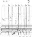
- Fig. 7 is a graphical representation of a comparison of the performance of SAW ladder filters including series and parallel resonators, based on resonators with and without piezoelectric trenches and heavy-metal electrodes illustrating extended high-frequency range, according to aspects of the present disclosure.
- Fig. 10 is a cross-sectional side view of a SAW resonator 1000 with a piezoelectric trench and heavy metal electrodes wherein the thickness of the heavy metal layers is varied between electrodes, according to aspects of the present disclosure.
- a SAW resonator may include spurious content above and below the fundamental resonance frequency. This leads to spurious content outside the passband of a filter which may interfere with the pass bands of other filters. Modulating the thickness of the heavy metal layers of different electrodes within a SAW resonator, as shown in Fig. 10 may advantageously reduce the amplitude of spurious content. In some aspects, the amplitude of spurious content may additionally be decreased by varying or modulating the pitch between electrodes (i.e., the distance between electrodes) as well as by modulating the depth of piezoelectric trenches.
- some electrodes may provide advantages at the expense of other performance metrics while others provide different advantages.
- some electrodes within a SAW resonator may be designed to achieve moderate stop band width while providing ideal coupling, while other electrodes within the same SAW resonator may be designed to achieve ideal stop band width with moderate coupling.
- This type of variation in electrodes may be implemented between different filters on the same die, between different groups of resonators within the same filter (e.g., series resonators or parallel resonators, also known as shunt resonators), or between different electrodes within the same resonator.
- the SAW resonator 1000 includes a carrier substrate 1045, a dielectric layer 1040, a dielectric layer 1035, and a piezoelectric film 1030.
- the SAW resonator includes electrodes 1026a, 1026b, 1026c, 1026d, and 1026e. Each of these electrodes includes heavy metal layers of differing thicknesses.
- the electrode 1026a includes a heavy metal layer of a thickness 1028a.
- the electrode 1026b includes a heavy metal layer of a thickness 1028b, greater than 1028a.
- the electrode 1026c includes a heavy metal layer of a thickness 1028c, greater than 1028a.
- the electrode 1026d includes a heavy metal layer of a thickness 1028d, greater than 1028a.
- Fig. 11 is a cross-sectional side view of a SAW resonator with piezoelectric trenches and heavy metal electrodes wherein the depth of the piezoelectric trenches is modulated, according to aspects of the present disclosure.
- the depth of piezoelectric trenches between electrodes may be varied by providing a continuous angled top surface of the piezoelectric trenches formed within the piezoelectric layer 1130.
- the SAW resonator 1100 includes a carrier substrate 1145, a dielectric layer 1140, a dielectric layer 1135, and a piezoelectric film 1130.
- the SAW resonator includes electrodes 1126a, 1126b, 1126c, 1126d, and 1126e.
- a piezoelectric trench is positioned between each of the electrodes 1126a.
- a piezoelectric trench 1170a is shown between the electrodes 1126a and 1126b.
- a piezoelectric trench 1170b is shown between the electrodes 1126b and 1126c.
- a piezoelectric trench 1170c is shown between the electrodes 1126c and 1126d.
- a piezoelectric trench 1170d is shown between the electrodes 1126d and 1126e.
- the depth of the piezoelectric trenches 1170 may be varied or modulated. This variation of the piezoelectric trench depth may be achieved due to the top surface of the piezoelectric layer 1135 being angled, for example, by an angle 1190.
- this modulation of the piezoelectric trench depth may provide a number of advantages. For example, PZTs of lesser thickness may correspond to regions of the resonator of higher capacitance per area, while PZTs of greater thickness correspond to regions of greater reflectivity. Thus, having PZTs of both greater and lesser depths may provide both advantages within the same resonator.
- this trench depth modulation may provide more continuity from unit cell to unit cell, leading to less scattering.
- the SAW resonator device includes a first electrode positioned on an upper surface of a piezoelectric film.
- the first electrode may include a plurality of layers wherein a layer of the plurality of layers is a first heavy metal layer.
- the SAW resonator device may also include a first piezoelectric trench (PZT) positioned adjacent to the first electrode.
- the first PZT includes a recess in the piezoelectric film.
Landscapes
- Physics & Mathematics (AREA)
- Acoustics & Sound (AREA)
- Engineering & Computer Science (AREA)
- Manufacturing & Machinery (AREA)
- Surface Acoustic Wave Elements And Circuit Networks Thereof (AREA)
Applications Claiming Priority (1)
| Application Number | Priority Date | Filing Date | Title |
|---|---|---|---|
| US202363582176P | 2023-09-12 | 2023-09-12 |
Publications (2)
| Publication Number | Publication Date |
|---|---|
| EP4583402A2 true EP4583402A2 (de) | 2025-07-09 |
| EP4583402A3 EP4583402A3 (de) | 2025-12-03 |
Family
ID=92675999
Family Applications (1)
| Application Number | Title | Priority Date | Filing Date |
|---|---|---|---|
| EP24198489.7A Pending EP4583402A3 (de) | 2023-09-12 | 2024-09-04 | Saw resonator mit schwermetallelektroden, zwischen denen gräben im piezoelektrischen material angeordnet sind |
Country Status (3)
| Country | Link |
|---|---|
| US (1) | US20250088175A1 (de) |
| EP (1) | EP4583402A3 (de) |
| CN (1) | CN119628591A (de) |
Cited By (1)
| Publication number | Priority date | Publication date | Assignee | Title |
|---|---|---|---|---|
| US20230327642A1 (en) * | 2022-04-08 | 2023-10-12 | Skyworks Solutions, Inc. | Acoustic wave device with trench portions for transverse mode suppression |
Family Cites Families (10)
| Publication number | Priority date | Publication date | Assignee | Title |
|---|---|---|---|---|
| WO2002035702A1 (en) * | 2000-10-23 | 2002-05-02 | Matsushita Electric Industrial Co., Ltd. | Surface acoustic wave filter |
| JP2013106089A (ja) * | 2011-11-10 | 2013-05-30 | Murata Mfg Co Ltd | 弾性波装置の製造方法 |
| US20170104470A1 (en) * | 2015-10-09 | 2017-04-13 | Avago Technologies General Ip (Singapore) Pte. Ltd. | Interdigitated transducers and reflectors for surface acoustic wave devices with non-uniformly spaced elements |
| US10389391B2 (en) * | 2016-01-29 | 2019-08-20 | Kyocera Corporation | Acoustic wave resonator, acoustic wave filter, multiplexer, and communication apparatus |
| JP2017224890A (ja) * | 2016-06-13 | 2017-12-21 | 株式会社村田製作所 | 弾性波装置 |
| KR102671258B1 (ko) * | 2018-07-27 | 2024-06-03 | 소이텍 | 공동 공진 saw 필터 |
| CN112039460B (zh) * | 2019-07-19 | 2022-05-10 | 中芯集成电路(宁波)有限公司 | 薄膜体声波谐振器及其制作方法 |
| CN113726307B (zh) * | 2021-08-18 | 2024-01-23 | 武汉敏声新技术有限公司 | 有效机电耦合系数可调的超高频谐振器 |
| US20230327642A1 (en) * | 2022-04-08 | 2023-10-12 | Skyworks Solutions, Inc. | Acoustic wave device with trench portions for transverse mode suppression |
| WO2024238156A2 (en) * | 2023-05-18 | 2024-11-21 | Qorvo Us, Inc. | Piezoelectric trenches interleaved with electrodes of a saw resonator for improved performance |
-
2024
- 2024-08-06 US US18/795,978 patent/US20250088175A1/en active Pending
- 2024-09-04 EP EP24198489.7A patent/EP4583402A3/de active Pending
- 2024-09-12 CN CN202411276010.8A patent/CN119628591A/zh active Pending
Cited By (1)
| Publication number | Priority date | Publication date | Assignee | Title |
|---|---|---|---|---|
| US20230327642A1 (en) * | 2022-04-08 | 2023-10-12 | Skyworks Solutions, Inc. | Acoustic wave device with trench portions for transverse mode suppression |
Also Published As
| Publication number | Publication date |
|---|---|
| CN119628591A (zh) | 2025-03-14 |
| US20250088175A1 (en) | 2025-03-13 |
| EP4583402A3 (de) | 2025-12-03 |
Similar Documents
| Publication | Publication Date | Title |
|---|---|---|
| US12289100B2 (en) | Resonant cavity surface acoustic wave (SAW) filters | |
| US12341491B2 (en) | Loaded resonators for adjusting frequency response of acoustic wave resonators | |
| TWI697204B (zh) | 複合基板上的表面聲波裝置 | |
| US6774746B2 (en) | Thin film bulk acoustic resonator filters with a piezoelectric layer of lead scandium tantalum oxide | |
| CN100571030C (zh) | 压电谐振滤波器和双工器 | |
| EP1575165B1 (de) | Akustischer Volumenwellen - Filter und Verfahren zur Vermeidung unerwünschter Seitendurchgänge | |
| WO2020161283A1 (en) | Low loss acoustic device | |
| EP3599720B1 (de) | Filter akustisch gekoppelter oberflächenwellenresonatoren | |
| TWI908923B (zh) | 聲波裝置中之壓電層配置及相關方法 | |
| JP7787066B2 (ja) | 音響波共振器の周波数応答を調整するための負荷をかけられた直列共振器 | |
| US20250088175A1 (en) | Piezoelectric trenches interleaved with heavy-metal electrodes of a saw resonator | |
| JP6798562B2 (ja) | ラダー型フィルタ、デュプレクサ及び弾性波フィルタ装置 | |
| CN111095794B (zh) | 一种表面声波器件 | |
| US8354896B2 (en) | Acoustic wave device, transmission apparatus, and acoustic wave device manufacturing method | |
| KR20250169194A (ko) | 개선된 성능을 위해 saw 공진기의 전극과 인터리브된 압전 트렌치 | |
| US20240380383A1 (en) | Surface Acoustic Wave Resonators With Interdigital Transducers Of Differing Duty Factor and Pitch | |
| HK40130256A (zh) | 用於提高性能的与saw谐振器的电极交错的压电沟槽 |
Legal Events
| Date | Code | Title | Description |
|---|---|---|---|
| PUAI | Public reference made under article 153(3) epc to a published international application that has entered the european phase |
Free format text: ORIGINAL CODE: 0009012 |
|
| STAA | Information on the status of an ep patent application or granted ep patent |
Free format text: STATUS: THE APPLICATION HAS BEEN PUBLISHED |
|
| AK | Designated contracting states |
Kind code of ref document: A2 Designated state(s): AL AT BE BG CH CY CZ DE DK EE ES FI FR GB GR HR HU IE IS IT LI LT LU LV MC ME MK MT NL NO PL PT RO RS SE SI SK SM TR |
|
| PUAL | Search report despatched |
Free format text: ORIGINAL CODE: 0009013 |
|
| AK | Designated contracting states |
Kind code of ref document: A3 Designated state(s): AL AT BE BG CH CY CZ DE DK EE ES FI FR GB GR HR HU IE IS IT LI LT LU LV MC ME MK MT NL NO PL PT RO RS SE SI SK SM TR |
|
| RIC1 | Information provided on ipc code assigned before grant |
Ipc: H03H 3/10 20060101AFI20251024BHEP Ipc: H03H 9/02 20060101ALI20251024BHEP Ipc: H03H 9/145 20060101ALI20251024BHEP Ipc: H03H 9/64 20060101ALI20251024BHEP |