EP4583384A1 - Elektronische vorrichtung und betriebsverfahren dafür - Google Patents
Elektronische vorrichtung und betriebsverfahren dafür Download PDFInfo
- Publication number
- EP4583384A1 EP4583384A1 EP24794325.1A EP24794325A EP4583384A1 EP 4583384 A1 EP4583384 A1 EP 4583384A1 EP 24794325 A EP24794325 A EP 24794325A EP 4583384 A1 EP4583384 A1 EP 4583384A1
- Authority
- EP
- European Patent Office
- Prior art keywords
- switch
- capacitor
- electronic device
- converter
- load
- Prior art date
- Legal status (The legal status is an assumption and is not a legal conclusion. Google has not performed a legal analysis and makes no representation as to the accuracy of the status listed.)
- Pending
Links
Images


Classifications
-
- H—ELECTRICITY
- H02—GENERATION; CONVERSION OR DISTRIBUTION OF ELECTRIC POWER
- H02M—APPARATUS FOR CONVERSION BETWEEN AC AND AC, BETWEEN AC AND DC, OR BETWEEN DC AND DC, AND FOR USE WITH MAINS OR SIMILAR POWER SUPPLY SYSTEMS; CONVERSION OF DC OR AC INPUT POWER INTO SURGE OUTPUT POWER; CONTROL OR REGULATION THEREOF
- H02M3/00—Conversion of DC power input into DC power output
- H02M3/02—Conversion of DC power input into DC power output without intermediate conversion into AC
- H02M3/04—Conversion of DC power input into DC power output without intermediate conversion into AC by static converters
- H02M3/06—Conversion of DC power input into DC power output without intermediate conversion into AC by static converters using resistors or capacitors, e.g. potential divider
- H02M3/07—Conversion of DC power input into DC power output without intermediate conversion into AC by static converters using resistors or capacitors, e.g. potential divider using capacitors charged and discharged alternately by semiconductor devices with control electrode, e.g. charge pumps
-
- G—PHYSICS
- G04—HOROLOGY
- G04G—ELECTRONIC TIME-PIECES
- G04G21/00—Input or output devices integrated in time-pieces
-
- G—PHYSICS
- G06—COMPUTING OR CALCULATING; COUNTING
- G06F—ELECTRIC DIGITAL DATA PROCESSING
- G06F1/00—Details not covered by groups G06F3/00 - G06F13/00 and G06F21/00
- G06F1/16—Constructional details or arrangements
- G06F1/1613—Constructional details or arrangements for portable computers
- G06F1/163—Wearable computers, e.g. on a belt
-
- G—PHYSICS
- G06—COMPUTING OR CALCULATING; COUNTING
- G06F—ELECTRIC DIGITAL DATA PROCESSING
- G06F1/00—Details not covered by groups G06F3/00 - G06F13/00 and G06F21/00
- G06F1/26—Power supply means, e.g. regulation thereof
-
- H—ELECTRICITY
- H02—GENERATION; CONVERSION OR DISTRIBUTION OF ELECTRIC POWER
- H02M—APPARATUS FOR CONVERSION BETWEEN AC AND AC, BETWEEN AC AND DC, OR BETWEEN DC AND DC, AND FOR USE WITH MAINS OR SIMILAR POWER SUPPLY SYSTEMS; CONVERSION OF DC OR AC INPUT POWER INTO SURGE OUTPUT POWER; CONTROL OR REGULATION THEREOF
- H02M1/00—Details of apparatus for conversion
- H02M1/0067—Converter structures employing plural converter units, other than for parallel operation of the units on a single load
- H02M1/007—Plural converter units in cascade
-
- H—ELECTRICITY
- H02—GENERATION; CONVERSION OR DISTRIBUTION OF ELECTRIC POWER
- H02M—APPARATUS FOR CONVERSION BETWEEN AC AND AC, BETWEEN AC AND DC, OR BETWEEN DC AND DC, AND FOR USE WITH MAINS OR SIMILAR POWER SUPPLY SYSTEMS; CONVERSION OF DC OR AC INPUT POWER INTO SURGE OUTPUT POWER; CONTROL OR REGULATION THEREOF
- H02M1/00—Details of apparatus for conversion
- H02M1/0083—Converters characterised by their input or output configuration
- H02M1/009—Converters characterised by their input or output configuration having two or more independently controlled outputs
-
- H—ELECTRICITY
- H02—GENERATION; CONVERSION OR DISTRIBUTION OF ELECTRIC POWER
- H02M—APPARATUS FOR CONVERSION BETWEEN AC AND AC, BETWEEN AC AND DC, OR BETWEEN DC AND DC, AND FOR USE WITH MAINS OR SIMILAR POWER SUPPLY SYSTEMS; CONVERSION OF DC OR AC INPUT POWER INTO SURGE OUTPUT POWER; CONTROL OR REGULATION THEREOF
- H02M3/00—Conversion of DC power input into DC power output
- H02M3/02—Conversion of DC power input into DC power output without intermediate conversion into AC
- H02M3/04—Conversion of DC power input into DC power output without intermediate conversion into AC by static converters
- H02M3/06—Conversion of DC power input into DC power output without intermediate conversion into AC by static converters using resistors or capacitors, e.g. potential divider
-
- H—ELECTRICITY
- H02—GENERATION; CONVERSION OR DISTRIBUTION OF ELECTRIC POWER
- H02M—APPARATUS FOR CONVERSION BETWEEN AC AND AC, BETWEEN AC AND DC, OR BETWEEN DC AND DC, AND FOR USE WITH MAINS OR SIMILAR POWER SUPPLY SYSTEMS; CONVERSION OF DC OR AC INPUT POWER INTO SURGE OUTPUT POWER; CONTROL OR REGULATION THEREOF
- H02M3/00—Conversion of DC power input into DC power output
- H02M3/02—Conversion of DC power input into DC power output without intermediate conversion into AC
- H02M3/04—Conversion of DC power input into DC power output without intermediate conversion into AC by static converters
- H02M3/10—Conversion of DC power input into DC power output without intermediate conversion into AC by static converters using discharge tubes with control electrode or semiconductor devices with control electrode
- H02M3/145—Conversion of DC power input into DC power output without intermediate conversion into AC by static converters using discharge tubes with control electrode or semiconductor devices with control electrode using devices of a triode or transistor type requiring continuous application of a control signal
- H02M3/155—Conversion of DC power input into DC power output without intermediate conversion into AC by static converters using discharge tubes with control electrode or semiconductor devices with control electrode using devices of a triode or transistor type requiring continuous application of a control signal using semiconductor devices only
- H02M3/156—Conversion of DC power input into DC power output without intermediate conversion into AC by static converters using discharge tubes with control electrode or semiconductor devices with control electrode using devices of a triode or transistor type requiring continuous application of a control signal using semiconductor devices only with automatic control of output voltage or current, e.g. switching regulators
- H02M3/158—Conversion of DC power input into DC power output without intermediate conversion into AC by static converters using discharge tubes with control electrode or semiconductor devices with control electrode using devices of a triode or transistor type requiring continuous application of a control signal using semiconductor devices only with automatic control of output voltage or current, e.g. switching regulators including plural semiconductor devices as final control devices for a single load
-
- G—PHYSICS
- G09—EDUCATION; CRYPTOGRAPHY; DISPLAY; ADVERTISING; SEALS
- G09G—ARRANGEMENTS OR CIRCUITS FOR CONTROL OF INDICATING DEVICES USING STATIC MEANS TO PRESENT VARIABLE INFORMATION
- G09G2330/00—Aspects of power supply; Aspects of display protection and defect management
-
- G—PHYSICS
- G09—EDUCATION; CRYPTOGRAPHY; DISPLAY; ADVERTISING; SEALS
- G09G—ARRANGEMENTS OR CIRCUITS FOR CONTROL OF INDICATING DEVICES USING STATIC MEANS TO PRESENT VARIABLE INFORMATION
- G09G3/00—Control arrangements or circuits, of interest only in connection with visual indicators other than cathode-ray tubes
- G09G3/20—Control arrangements or circuits, of interest only in connection with visual indicators other than cathode-ray tubes for presentation of an assembly of a number of characters, e.g. a page, by composing the assembly by combination of individual elements arranged in a matrix no fixed position being assigned to or needed to be assigned to the individual characters or partial characters
- G09G3/22—Control arrangements or circuits, of interest only in connection with visual indicators other than cathode-ray tubes for presentation of an assembly of a number of characters, e.g. a page, by composing the assembly by combination of individual elements arranged in a matrix no fixed position being assigned to or needed to be assigned to the individual characters or partial characters using controlled light sources
- G09G3/30—Control arrangements or circuits, of interest only in connection with visual indicators other than cathode-ray tubes for presentation of an assembly of a number of characters, e.g. a page, by composing the assembly by combination of individual elements arranged in a matrix no fixed position being assigned to or needed to be assigned to the individual characters or partial characters using controlled light sources using electroluminescent panels
- G09G3/32—Control arrangements or circuits, of interest only in connection with visual indicators other than cathode-ray tubes for presentation of an assembly of a number of characters, e.g. a page, by composing the assembly by combination of individual elements arranged in a matrix no fixed position being assigned to or needed to be assigned to the individual characters or partial characters using controlled light sources using electroluminescent panels semiconductive, e.g. using light-emitting diodes [LED]
- G09G3/3208—Control arrangements or circuits, of interest only in connection with visual indicators other than cathode-ray tubes for presentation of an assembly of a number of characters, e.g. a page, by composing the assembly by combination of individual elements arranged in a matrix no fixed position being assigned to or needed to be assigned to the individual characters or partial characters using controlled light sources using electroluminescent panels semiconductive, e.g. using light-emitting diodes [LED] organic, e.g. using organic light-emitting diodes [OLED]
Definitions
- the disclosure relates to an electronic device and a method for operating the same.
- a circuit responsible for light emission of an organic light emitting diode (OLED) driver may include a light emitting diode (LED) that emits light when current flows, and a switch (e.g., a field effect transistor (FET)) that controls the current flowing through the LED.
- a switch e.g., a field effect transistor (FET)
- FET field effect transistor
- the voltage may be formed based on a ground rather than a floated state. For example, with the top (e.g. first terminal, anode terminal, or anode) of the LED connected to the bottom (e.g. second terminal, source terminal, or source) of the FET, the bottom of the FET may be connected to the ground of a system. Therefore, when a voltage supplied to the top (e.g.
- first terminal, drain terminal, or drain of the FET is VELVDD and a voltage supplied to the bottom (e.g. second terminal, cathode terminal, or cathode) of the LED is VELVSS, power with VELVDD>0 and VELVSS ⁇ 0 needs to be supplied.
- a negative voltage is not needed.
- voltages for driving the FET and the LED are accumulated in series, there is a problem in that a high voltage corresponding to the sum of the two voltages is to be supplied. Except for some products, therefore, a structure that may avoid the high voltage issue by separately supplying positive and negative voltages with respect to the ground is selected.
- a switching regulator (or switching converter) is a circuit that converts a direct current (DC) voltage into a DC voltage, and a buck converter is used for step-down, a boost converter for step-up, and a non-inverting buck-boost converter for both step-up and step-down.
- an electronic device includes a power conversion circuit and a load configured to receive power from the power conversion circuit.
- the power conversion circuit includes a converter including an inductor, a first switch, and a second switch.
- the power conversion circuit includes a charge pump including a third switch, a fourth switch, a first capacitor, a fifth switch, and a sixth switch.
- the power conversion circuit includes a second capacitor, a first active dummy load connected in parallel with the second capacitor, a third capacitor, and a second active dummy load connected in parallel with the third capacitor.
- a method for operating an electronic device includes controlling switches of a converter of the electronic device and switches of a charge pump connected in parallel with the converter.
- the converter includes an inductor, a first switch, and a second switch.
- the charge pump includes a third switch, a fourth switch, a first capacitor, a fifth switch, and a sixth switch.
- the method includes controlling a first active dummy load connected in parallel with a second capacitor of the electronic device or controlling a second active dummy load connected in parallel with a third capacitor of the electronic device.
- the at least one operation includes controlling switches of a converter of the electronic device and switches of a charge pump connected in parallel with the converter.
- the converter includes an inductor, a first switch, and a second switch.
- the charge pump includes a third switch, a fourth switch, a first capacitor, a fifth switch, and a sixth switch.
- the at least one operation includes controlling a first active dummy load connected in parallel with a second capacitor of the electronic device or controlling a second active dummy load connected in parallel with a third capacitor of the electronic device.
- FIG. 1 is a block diagram illustrating an electronic device in a network environment according to an embodiment.
- an electronic device 101 in a network environment 100 may communicate with an electronic device 102 via a first network 198 (e.g., a short-range wireless communication network), or at least one of an electronic device 104 or a server 108 via a second network 199 (e.g., a long-range wireless communication network).
- the electronic device 101 may communicate with the electronic device 104 via the server 108.
- the electronic device 101 may include a processor 120, memory 130, an input module 150, a sound output module 155, a display module 160, an audio module 170, a sensor module 176, an interface 177, a connecting terminal 178, a haptic module 179, a camera module 180, a power management module 188, a battery 189, a communication module 190, a subscriber identification module (SIM) 196, or an antenna module 197.
- at least one of the components e.g., the connecting terminal 178) may be omitted from the electronic device 101, or one or more other components may be added in the electronic device 101.
- some of the components e.g., the sensor module 176, the camera module 180, or the antenna module 197) may be implemented as a single component (e.g., the display module 160).
- the auxiliary processor 123 may control at least some of functions or states related to at least one component (e.g., the display module 160, the sensor module 176, or the communication module 190) among the components of the electronic device 101, instead of the main processor 121 while the main processor 121 is in an inactive (e.g., sleep) state, or together with the main processor 121 while the main processor 121 is in an active state (e.g., executing an application).
- the auxiliary processor 123 e.g., an image signal processor or a communication processor
- the memory 130 may store various data used by at least one component (e.g., the processor 120 or the sensor module 176) of the electronic device 101.
- the various data may include, for example, software (e.g., the program 140) and input data or output data for a command related thereto.
- the memory 130 may include the volatile memory 132 or the non-volatile memory 134.
- the program 140 may be stored in the memory 130 as software, and may include, for example, an operating system (OS) 142, middleware 144, or an application 146.
- OS operating system
- middleware middleware
- application application
- the input module 150 may receive a command or data to be used by another component (e.g., the processor 120) of the electronic device 101, from the outside (e.g., a user) of the electronic device 101.
- the input module 150 may include, for example, a microphone, a mouse, a keyboard, a key (e.g., a button), or a digital pen (e.g., a stylus pen).
- the display module 160 may visually provide information to the outside (e.g., a user) of the electronic device 101.
- the display module 160 may include, for example, a display, a hologram device, or a projector and control circuitry to control a corresponding one of the display, hologram device, and projector.
- the display module 160 may include a touch sensor adapted to detect a touch, or a pressure sensor adapted to measure the strength of force incurred by the touch.
- the audio module 170 may convert a sound into an electrical signal and vice versa. According to an embodiment, the audio module 170 may obtain the sound via the input module 150, or output the sound via the sound output module 155 or a headphone of an external electronic device (e.g., an electronic device 102) directly (e.g., wiredly) or wirelessly coupled with the electronic device 101.
- an external electronic device e.g., an electronic device 102
- directly e.g., wiredly
- wirelessly e.g., wirelessly
- the sensor module 176 may detect an operational state (e.g., power or temperature) of the electronic device 101 or an environmental state (e.g., a state of a user) external to the electronic device 101, and then generate an electrical signal or data value corresponding to the detected state.
- the sensor module 176 may include, for example, a gesture sensor, a gyro sensor, an atmospheric pressure sensor, a magnetic sensor, an acceleration sensor, a grip sensor, a proximity sensor, a color sensor, an infrared (IR) sensor, a biometric sensor, a temperature sensor, a humidity sensor, or an illuminance sensor.
- the interface 177 may support one or more specified protocols to be used for the electronic device 101 to be coupled with the external electronic device (e.g., the electronic device 102) directly (e.g., wiredly) or wirelessly.
- the interface 177 may include, for example, a high definition multimedia interface (HDMI), a universal serial bus (USB) interface, a secure digital (SD) card interface, or an audio interface.
- HDMI high definition multimedia interface
- USB universal serial bus
- SD secure digital
- a connecting terminal 178 may include a connector via which the electronic device 101 may be physically connected with the external electronic device (e.g., the electronic device 102).
- the connecting terminal 178 may include, for example, a HDMI connector, a USB connector, a SD card connector, or an audio connector (e.g., a headphone connector).
- the camera module 180 may capture a still image or moving images.
- the camera module 180 may include one or more lenses, image sensors, image signal processors, or flashes.
- the communication module 190 may support establishing a direct (e.g., wired) communication channel or a wireless communication channel between the electronic device 101 and the external electronic device (e.g., the electronic device 102, the electronic device 104, or the server 108) and performing communication via the established communication channel.
- the communication module 190 may include one or more communication processors that are operable independently from the processor 120 (e.g., the application processor (AP)) and supports a direct (e.g., wired) communication or a wireless communication.
- AP application processor
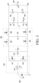
- the charge pump 320 may store power provided by the converter 310 or the capacitor 314 (e.g., C4 in FIG. 3 ) connected in parallel with the converter 310 in the first capacitor 321, based on operations (e.g., on/off) of the switches 323, 324, 325, and 326.
- the charge pump 320 may output power through the fifth switch 325 and the sixth switch 326 based on the power stored in the first capacitor 321, based on the operations (e.g., on/off) of the switches 323, 324, 325, and 326.
- the power stored in the first capacitor 321 of the charge pump 320 may be provided to capacitors (e.g., 331 and 341) connected to a rear end (or output end) of the charge pump 320, for example to capacitors connected in series with each other, between output terminals, or output rails, of the charge pump 320.
- the electronic device 101 e.g., the power conversion circuit 210) may include a second capacitor 331 and a third capacitor 341.
- the second capacitor 331 and the third capacitor 341 may be provided with the power stored in the first capacitor 321 based on the operations (e.g., on/off) of the switches 323, 324, 325, and 326 of the charge pump 320.
- the third capacitor 341 may be connected to the second capacitor 331 and the ground.
- the second capacitor 331 may store power corresponding to a positive voltage (e.g., V ELVDD in FIG. 3 ).
- the third capacitor 341 may store power corresponding to a negative voltage (e.g., V ELVSS in FIG. 3 ).
- the power corresponding to the positive voltage (e.g., V ELVDD in FIG. 3 ) stored in the second capacitor 331 may be provided to a first end (e.g. first terminal)(e.g., the N1 node) of the load 220 (e.g., 340 in FIGS. 3 and 5 ).
- the power corresponding to the negative voltage (e.g., V ELVSS in FIG. 3 ) stored in the third capacitor 341 may be provided to a second end (e.g.
- the N1 node may, for example, be described as being a terminal of, or a connection to, a first power rail (e.g. a first power supply rail, a first rail, a positive supply rail, a positive rail, or a high rail), and the N2 node may, for example, be described as being a terminal of, or a connection to, a second power rail (e.g. a second power supply rail, a second rail, a negative supply rail, a negative rail, or a low rail).
- a first power rail e.g. a first power supply rail, a first rail, a positive supply rail, a positive rail, or a high rail
- a second power rail e.g. a second power supply rail, a second rail, a negative supply rail, a negative rail, or a low rail.
- the electronic device 101 may include a first load 332 (e.g. a first active (i.e. controllable) load, or a first active dummy load 332) connected in parallel with the second capacitor 331 (e.g., a shunt capacitor), and a second load 342 (e.g. a second active (i.e. controllable) load, or a second active dummy load 342) connected in parallel with the third capacitor 341 (e.g., a shunt capacitor).
- the load (e.g. active dummy load) 332 or 342 may be configured to control a voltage of the capacitor 331 or 341 connected in parallel therewith.
- the second active dummy load 342 may include a circuit that causes a similar effect to that of the switch 422 without including the switch 422.
- Controlling the active dummy load 332 or 342 may include controlling the switch 412 or 422 of the active dummy load 332 or 342.
- the electronic device 101 e.g., the controller 120
- a first end of the inductor 313 of the converter 310 may be connected to a first end of the first switch 311 of the converter 310 and a first end of the second switch 312 of the converter 310.
- the term “end” may alternatively be replaced by the term “terminal”, and so this disclosure includes disclosure of subject matter corresponding to all of the text of this specification, but with the term “end” replaced by "terminal”.
- a second end of the inductor 313 may be connected to the power source 300.
- a second end of the first switch 311 of the converter 310 may be connected to a first end of the third switch 323 of the charge pump 320.
- a second end of the second switch 312 of the converter 310 may be connected to a first end of the fourth switch 324 of the charge pump 320 and the ground.
- a second end of the third switch 323 of the charge pump 320 may be connected to a first end of the fifth switch 325 of the charge pump 320 and a first end of the first capacitor 321 of the charge pump 320.
- a second end of the fourth switch 324 of the charge pump 320 may be connected to a first end of the sixth switch 326 of the charge pump 320 and a second end of the first capacitor 321 of the charge pump 320.
- a second end of the fifth switch 325 of the charge pump 320 may be connected to a first end of the second capacitor 331 and a first end of the first active dummy load 332.
- FIG. 6 is a diagram illustrating an electronic device according to an embodiment.
- the electronic device 101 may be a wearable device 600.
- the electronic device 101 e.g., the wearable device 600
- the electronic device 101 may include a housing 610, a display 660 (e.g., the display module 160 in FIG. 1 ), and a strap 620.
- the strap 620 may be configured to mount the electronic device 101 (e.g., the wearable device 600) on a user's wrist.
- the load 220 e.g., 340 in FIGS.
- At least some of the operations in FIG. 7 may be omitted.
- the order of the operations in FIG. 7 may be changed.
- An operation other than the operations of FIG. 7 may be performed before, during, or after the operations of FIG. 7 .
- the electronic device 101 may control the first switch 311 of the converter 310, the third switch 323 of the charge pump, and the fourth switch 324 of the charge pump 320 to be on, and control the second switch 312 of the converter 310, the fifth switch 325 of the charge pump 320, and the sixth switch 326 of the charge pump 320 to be off, during a first period.
- the electronic device 101 e.g., the controller 120
- the capacitance of the fourth capacitor 314 of FIG. 3 may be minimized or the fourth capacitor 314 may be removed.
- the electronic device 101 may not include the fourth capacitor 314 of FIG. 3 .
- the electronic device 101 may perform the operations of FIG. 7 without including the fourth capacitor 314 of FIG. 3 .
- an input current of the converter 310 is continuously input, an output current of the converter 310 may be output only while the first switch 311 is on, and the output current of the converter 310 may be zero while the second switch 312 is on.
- the electronic device 101 may control the third switch 323 and fourth switch 324 of the charge pump 320 to be on while the first switch 311 of the converter 310 is on. Accordingly, the first capacitor 321 functions even as a boost capacitor (e.g., the fourth capacitor 314), and as a result, the fourth capacitor 314 may not be included in the electronic device 101.
- the electronic device 101 may include a fourth capacitor 314 having a capacity decreased by as much as the capacity (e.g., capacitance) of the first capacitor 321.
- the structure of the power conversion circuit 210 in FIG. 3 may improve power conversion efficiency compared to an existing method.
- Executing the converter 310 may include starting the operation of the converter 310, changing the operation of the converter 310, or maintaining the operation of the converter 310.
- Starting the operation of the converter 310 may be to apply a pulse width modulation (PWM) control signal to the switches 311 and 312 of the converter 310.
- Changing the operation of the converter 310 may be to change the PWM control signal applied to the switches 311 and 312 of the converter 310.
- the electronic device 101 e.g., the controller 120
- the electronic device 101 may control the first active dummy load 332 to be on, based on the voltage (e.g., V ELVDD in FIG. 3 ) of the second capacitor 331 being greater than the first target voltage (e.g., positive voltage).
- the electronic device 101 e.g., the controller 120
- the switch e.g., 412
- the voltage e.g., V ELVDD in FIG. 3
- the voltage e.g., V ELVDD in FIG. 3
- the decrease of the voltage being a positive voltage may be a decrease in the absolute value of the voltage.
- the electronic device 101 may control the first active dummy load 332 to be off, based on the voltage (e.g., V ELVDD in FIG. 3 ) of the second capacitor 331 being equal to or less than the first target voltage (e.g., positive voltage).
- the electronic device 101 e.g., the controller 120
- the switch e.g., 412 of the first active dummy load 332 to be off, based on the voltage (e.g., V ELVDD in FIG. 3 ) of the second capacitor 331 being equal to or less than the first target voltage.
- At least some of the operations of FIG. 10 may be omitted.
- the order of the operations in FIG. 10 may be changed.
- An operation other than the operations of FIG. 10 may be performed before, during, or after the operations of FIG. 10 .
- FIG. 10 may be performed simultaneously with or separately from the operations of FIGS. 7 and 8 .
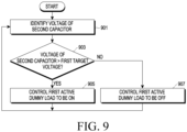
- the electronic device 101 may identify a voltage (e.g., V ELVSS in FIG. 3 ) of the third capacitor 341.
- the electronic device 101 may compare the voltage (e.g., V ELVSS in FIG. 3 ) of the third capacitor 341 with a second target voltage.
- the second target voltage may be a target value for a voltage corresponding to the third capacitor 341.
- the second target voltage may be a target value for a voltage to be provided to the first end (e.g., the N2 node) of the LED 510 of the load 220 (e.g., 340 in FIGS. 3 and 5 ).
- the second target voltage may be a negative voltage.
- the electronic device 101 may control the second active dummy load 342 to be on, based on the voltage (e.g., V ELVSS in FIG. 3 ) of the third capacitor 341 being less than the second target voltage (e.g., negative voltage).
- the electronic device 101 e.g., the controller 120
- the switch (e.g., 422) of the second active dummy load 342 may be on, based on the voltage (e.g., V ELVSS in FIG. 3 ) of the third capacitor 341 being less than the second target voltage.
- the voltage (e.g., V ELVSS in FIG. 3 ) (e.g., negative voltage) of the third capacitor 341 connected in parallel with the second active dummy load 342 may increase.
- the increase of the voltage being a negative voltage may be a decrease in the absolute value of the voltage.
- the electronic device 101 may control the second active dummy load 342 to be off, based on the voltage (e.g., V ELVSS in FIG. 3 ) of the third capacitor 341 being equal to or greater than the second target voltage (e.g., negative voltage).
- the electronic device 101 e.g., the controller 120
- the switch e.g., 422 of the second active dummy load 342 to be off, based on the voltage (e.g., V ELVSS in FIG. 3 ) of the third capacitor 341 being equal to or greater than the second target voltage.
- the electronic device 101 or 600 may include the power conversion circuit 210 and the load 220 or 340 configured to receive power from the power conversion circuit 210.
- the power conversion circuit 210 may include the converter 310 including the inductor 313, the first switch 311, and the second switch 312.
- the charge pump 320 may include the third switch 323, the fourth switch 324, the first capacitor 321, the fifth switch 325, and the sixth switch 326.
- the power conversion circuit 210 may include the second capacitor 331, a first active (e.g. controllable) load 332 (e.g. the first active dummy load 332) connected in parallel with the second capacitor 331, the third capacitor 341, and a second active (e.g. controllable) load 342 (e.g. the second active dummy load 342) connected in parallel with the third capacitor 341.
- the first end of the inductor 313 may be connected to the first end of the first switch 311 and the first end of the second switch 312.
- the second end of the first switch 311 may be connected to the first end of the third switch 323.
- the second end of the second switch 312 may be connected to the first end of the fourth switch 324 and the ground.
- the second end of the third switch 323 may be connected to the first end of the fifth switch 325 and the first end of the first capacitor 321.
- the second end of the fourth switch 324 may be connected to the first end of the sixth switch 326 and the second end of the first capacitor 321.
- the second end of the fifth switch 325 may be connected to the first end of the second capacitor 321 and the first end of the first active load 332 (e.g.
- the second end of the sixth switch 326 may be connected to the first end of the third capacitor 341 and the first end of the second active load 342 (e.g. the second active dummy load 342).
- the second end of the second capacitor 331 may be connected to the second end of the first active (e.g. dummy) load 332, the second end of the second active (e.g. dummy) load 342, the second end of the third capacitor 341, and the ground.
- the first end of the load 220 or 340 may be connected to the first end of the second capacitor 331.
- the second end of the load 220 or 340 may be connected to the first end of the third capacitor 341.
- the electronic device 101 or 600 may further include the fourth capacitor 314 connected in parallel with the converter 310 (for example between, or across, output terminals of the converter).
- the first end of the fourth capacitor 314 may be connected to the second end of the first switch 311 and the first end of the third switch 323.
- the second end of the fourth capacitor 314 may be connected to the second end of the second switch 312 and the first end of the fourth switch 324.
- the converter 310 may be a boost converter or a non-inverting buck-boost converter.
- the electronic device 101 or 600 may further include a controller 120 (e.g., the processor 120).
- the controller 120 may be configured to, during a first period, control the first switch 311, the third switch 323, and the fourth switch 324 to be on, and control the second switch 312, the fifth switch 325, and the sixth switch 326 to be off.
- the controller 120 may be configured to, during a second period, control the second switch 312, the fifth switch 325, and the sixth switch 326 to be on, and control the first switch 311, the third switch 323, and the fourth switch 324 to be off.
- the controller 120 may be configured to, during a third period, control the first switch 311, the second switch 312, the third switch 323, and the fourth switch 324 to be off, and control the fifth switch 325 and the sixth switch 326 to be on.
- the controller 120 may be configured to control an output of the converter 310 based on a sum of an absolute value of a first target voltage corresponding to the second capacitor 331 and an absolute value of a second target voltage corresponding to the third capacitor 341.
- the controller 120 may be configured to control the first active (e.g. dummy) load 332 to be on, based on a first voltage of the second capacitor 331 being greater than the first target voltage.
- the controller 120 may be configured to control the second active (e.g. dummy) load 342 to be on, based on a second voltage of the third capacitor 341 being less than the second target voltage.
- the first active (e.g. dummy) load 332 may include the first resistor 411 and the seventh switch 412.
- the second active (e.g. dummy) load 342 may include the second resistor 421 and the eighth switch 422.
- the first voltage of the second capacitor 331 may be provided to the first end of the load 220 or 340.
- the second voltage of the third capacitor 341 may be provided to the second end of the load 220 or 340.
- the load 220 or 340 may include the LED 510 and the ninth switch 520.
- the electronic device 101 or 600 may further include the strap 620 configured to mount the electronic device 101 or 600 on a user's wrist.
- a method for operating the electronic device 101 or 600 may include controlling the switches 311 and 312 of the converter 310 of the electronic device 101 or 600 and the switches 323, 324, 325, and 326 of the charge pump 320 connected in parallel with the converter 310.
- the converter 310 may include the inductor 313, the first switch 311, and the second switch 312.
- the charge pump 320 may include the third switch 323, the fourth switch 324, the first capacitor 321, the fifth switch 325, and the sixth switch 326.
- the method may include controlling the first active (e.g. dummy) load 332 connected in parallel with the second capacitor 331 of the electronic device 101 or 600 or controlling the second active (e.g. dummy) load 342 connected in parallel with the third capacitor 341 of the electronic device 101 or 600.
- controlling the switches 323, 324, 325, and 326 of the charge pump 320 may include providing a voltage of the first capacitor 321 to the second capacitor 331 and the third capacitor 341 by controlling the fifth switch 325 and the sixth switch 326 to be on.
- the first end of the fifth switch 325 may be connected to the first end of the first capacitor 321.
- the first end of the sixth switch 326 may be connected to the second end of the first capacitor 321.
- the first end of the second capacitor 331 may be connected to the second end of the fifth switch 325.
- the first end of the third capacitor 341 may be connected to the second end of the sixth switch 326.
- the second end of the second capacitor 331 may be connected to the second end of the third capacitor 341 and the ground.
- the electronic device 101 or 600 may further include the fourth capacitor 314 connected in parallel with the converter 310.
- controlling the switches 311 and 312 of the converter 310 and the switches 323, 324, 325, and 326 of the charge pump 320 may include, during a first period, controlling the first switch 311, the third switch 323, and the fourth switch 324 to be on, and controlling the second switch 312, the fifth switch 325, and the sixth switch 326 to be off.
- Controlling the switches 311 and 312 of the converter 310 and the switches 323, 324, 325, and 326 of the charge pump 320 may include, during a second period, controlling the second switch 312, the fifth switch 325, and the sixth switch 326 to be on, and controlling the first switch 311, the third switch 323, and the fourth switch 324 to be off.
- Controlling the switches 311 and 312 of the converter 310 and the switches 323, 324, 325, and 326 of the charge pump 320 may include, during a third period, controlling the first switch 311, the second switch 312, the third switch 323, and the fourth switch 324 to be off, and controlling the fifth switch 325 and the sixth switch 326 to be on.
- controlling the first active (e.g. dummy) load 332 or controlling the second active (e.g. dummy) load 342 may include controlling the first active (e.g. dummy) load 332 to be on,
- Controlling the first active (e.g. dummy) load 332 or controlling the second active (e.g. dummy) load 342 may include controlling the second active (e.g. dummy) load 342 to be on, based on a second voltage of the third capacitor 341 being less than the second target voltage.
- the first active (e.g. dummy) load 332 may include the first resistor 411 and the seventh switch 412.
- the at least one operation may include controlling the switches 311 and 312 of the converter 310 of the electronic device 101 or 600 and the switches 323, 324, 325, and 326 of the charge pump 320 connected in parallel with the converter 310.
- the converter 310 may include the inductor 313, the first switch 311, and the second switch 312.
- the charge pump 320 may include the third switch 323, the fourth switch 324, the first capacitor 321, the fifth switch 325, and the sixth switch 326.
- the at least one operation may include controlling the first active (e.g. dummy) load 332 connected in parallel with the second capacitor 331 of the electronic device 101 or 600 or controlling the second active (e.g. dummy) load 342 connected in parallel with the third capacitor 341 of the electronic device 101 or 600.
- the electronic device 101 or 600 may further include the fourth capacitor 314 connected in parallel with the converter 310.
- controlling the switches 311 and 312 of the converter 310 and the switches 323, 324, 325, and 326 of the charge pump 320 may include, during a first period, controlling the first switch 311, the third switch 323, and the fourth switch 324 to be on, and controlling the second switch 312, the fifth switch 325, and the sixth switch 326 to be off.
- Controlling the switches 311 and 312 of the converter 310 and the switches 323, 324, 325, and 326 of the charge pump 320 may include, during a second period, controlling the second switch 312, the fifth switch 325, and the sixth switch 326 to be on, and controlling the first switch 311, the third switch 323, and the fourth switch 324 to be off.
- Controlling the switches 311 and 312 of the converter 310 and the switches 323, 324, 325, and 326 of the charge pump 320 may include, during a third period, controlling the first switch 311, the second switch 312, the third switch 323, and the fourth switch 324 to be off, and controlling the fifth switch 325 and the sixth switch 326 to be on.
- controlling the switches 311 and 312 of the converter 310 may include controlling an output of the converter 310 based on a sum of an absolute value of a first target voltage corresponding to the second capacitor 331 and an absolute value of a second target voltage corresponding to the third capacitor 341.
- controlling the first active (e,g, dummy) load 332 or controlling the second active (e.g. dummy) load 342 may include controlling the first active (e.g. dummy) load 332 to be on,
- Controlling the first active (e.g. dummy) load 332 or controlling the second active (e.g. dummy) load 342 may include controlling the second active (e.g. dummy) load 342 to be on, based on a second voltage of the third capacitor 341 being less than the second target voltage.
- the first active (e.g. dummy) load 332 may include the first resistor 411 and the seventh switch 412.
- an element e.g., a first element
- the element may be coupled with the other element directly (e.g., wiredly), wirelessly, or via a third element.
- module may include a unit implemented in hardware, software, or firmware, and may interchangeably be used with other terms, for example, logic, logic block, part, or circuitry.
- a module may be a single integral component, or a minimum unit or part thereof, adapted to perform one or more functions.
- the module may be implemented in a form of an application-specific integrated circuit (ASIC).
- ASIC application-specific integrated circuit
- the machine-readable storage medium may be provided in the form of a non-transitory storage medium.
- non-transitory simply means that the storage medium is a tangible device, and does not include a signal (e.g., an electromagnetic wave), but this term does not differentiate between where data is semi-permanently stored in the storage medium and where the data is temporarily stored in the storage medium.
- each component e.g., a module or a program of the above-described components may include a single entity or multiple entities, and some of the multiple entities may be separately disposed in different components.
- one or more of the above-described components may be omitted, or one or more other components may be added.
- a plurality of components e.g., modules or programs
- the integrated component may still perform one or more functions of each of the plurality of components in the same or similar manner as they are performed by a corresponding one of the plurality of components before the integration.
- operations performed by the module, the program, or another component may be carried out sequentially, in parallel, repeatedly, or heuristically, or one or more of the operations may be executed in a different order or omitted, or one or more other operations may be added.
Landscapes
- Engineering & Computer Science (AREA)
- Power Engineering (AREA)
- Theoretical Computer Science (AREA)
- Physics & Mathematics (AREA)
- General Physics & Mathematics (AREA)
- Computer Hardware Design (AREA)
- General Engineering & Computer Science (AREA)
- Human Computer Interaction (AREA)
- Dc-Dc Converters (AREA)
Applications Claiming Priority (3)
| Application Number | Priority Date | Filing Date | Title |
|---|---|---|---|
| KR20230148127 | 2023-10-31 | ||
| KR1020230196600A KR20250063080A (ko) | 2023-10-31 | 2023-12-29 | 전자 장치 및 그 동작 방법 |
| PCT/KR2024/016807 WO2025095576A1 (ko) | 2023-10-31 | 2024-10-30 | 전자 장치 및 그 동작 방법 |
Publications (1)
| Publication Number | Publication Date |
|---|---|
| EP4583384A1 true EP4583384A1 (de) | 2025-07-09 |
Family
ID=93430472
Family Applications (1)
| Application Number | Title | Priority Date | Filing Date |
|---|---|---|---|
| EP24794325.1A Pending EP4583384A1 (de) | 2023-10-31 | 2024-10-30 | Elektronische vorrichtung und betriebsverfahren dafür |
Country Status (2)
| Country | Link |
|---|---|
| EP (1) | EP4583384A1 (de) |
| WO (1) | WO2025095576A1 (de) |
Family Cites Families (5)
| Publication number | Priority date | Publication date | Assignee | Title |
|---|---|---|---|---|
| JPH0539189U (ja) * | 1991-10-18 | 1993-05-25 | 新電元工業株式会社 | スイツチング電源のアクテイブダミ−回路 |
| US7977927B2 (en) * | 2007-08-08 | 2011-07-12 | Advanced Analogic Technologies, Inc. | Step-up DC/DC voltage converter with improved transient current capability |
| US9197129B2 (en) * | 2013-01-28 | 2015-11-24 | Qualcomm, Incorporated | Boost converter topology for high efficiency and low battery voltage support |
| JP6040899B2 (ja) * | 2013-04-08 | 2016-12-07 | ソニー株式会社 | 電子機器および給電システム |
| US10284090B2 (en) * | 2016-10-20 | 2019-05-07 | Cirrus Logic, Inc. | Combined boost converter and power converter |
-
2024
- 2024-10-30 EP EP24794325.1A patent/EP4583384A1/de active Pending
- 2024-10-30 WO PCT/KR2024/016807 patent/WO2025095576A1/ko active Pending
Also Published As
| Publication number | Publication date |
|---|---|
| WO2025095576A1 (ko) | 2025-05-08 |
Similar Documents
| Publication | Publication Date | Title |
|---|---|---|
| US12323044B2 (en) | 3-level-inverting buck-boost converter and control method thereof | |
| US20210036607A1 (en) | Power conversion device and method | |
| US20250293598A1 (en) | Electronic device for controlling dc/dc converter and method for operating the electronic device | |
| US20240396585A1 (en) | Method for controlling voltage supplied to rf transmission/reception module, and electronic device for carrying out same | |
| EP4583384A1 (de) | Elektronische vorrichtung und betriebsverfahren dafür | |
| KR20220134306A (ko) | 복수의 리니어 레귤레이터를 포함하는 레귤레이팅 회로 및 그의 동작 방법 | |
| KR102863278B1 (ko) | 부스트 회로를 포함하는 전자 장치 및 그 전자 장치의 제어 방법 | |
| US12499823B2 (en) | Electronic device comprising display, and operation method thereor | |
| KR20250063080A (ko) | 전자 장치 및 그 동작 방법 | |
| KR20230065847A (ko) | 전원 공급 회로를 포함하는 전자 장치 | |
| US11893931B2 (en) | Electronic device including power supply circuit | |
| US20250132589A1 (en) | Electronic device and method for controlling battery | |
| EP4394754A1 (de) | Elektronische vorrichtung mit anzeige und betriebsverfahren dafür | |
| KR20250025279A (ko) | 로드로 전력을 제공하는 컨버터를 포함하는 전자 장치 및 그 동작 방법 | |
| KR20240164344A (ko) | 디스플레이에 전원을 제공하는 전원 장치 및 제어 방법 | |
| KR20230173561A (ko) | 디스플레이를 포함하는 전자 장치와 이의 동작 방법 | |
| KR20250010467A (ko) | 전자 장치 및 그 동작 방법 | |
| US11855481B2 (en) | Electronic device including power management integrated circuit and operating method thereof | |
| KR20240067758A (ko) | 디스플레이를 포함하는 전자 장치와 이의 동작 방법 | |
| KR20250162269A (ko) | 논-인버팅 벅부스트 컨버터를 이용하여 바이어스 전압을 공급하는 전자 장치와 이의 동작 방법 | |
| KR20250032716A (ko) | 전자 장치 및 그 동작 방법 | |
| EP4636989A1 (de) | Elektronische vorrichtung und steuerungsverfahren für drahtgebundene/drahtlose ladung in einer elektronischen vorrichtung | |
| US20250149908A1 (en) | Electronic device comprising plurality of batteries and operating method therefor | |
| KR20250015658A (ko) | 전력 공급을 제어하기 위한 전자 장치, 방법 및 비 일시적 저장 매체 | |
| KR20250123635A (ko) | 스위치드 커패시터 컨버터, 스위치드 커패시터 컨버터를 포함하는 전자 장치 및 그 동작 방법 |
Legal Events
| Date | Code | Title | Description |
|---|---|---|---|
| STAA | Information on the status of an ep patent application or granted ep patent |
Free format text: STATUS: UNKNOWN |
|
| STAA | Information on the status of an ep patent application or granted ep patent |
Free format text: STATUS: THE INTERNATIONAL PUBLICATION HAS BEEN MADE |
|
| PUAI | Public reference made under article 153(3) epc to a published international application that has entered the european phase |
Free format text: ORIGINAL CODE: 0009012 |
|
| STAA | Information on the status of an ep patent application or granted ep patent |
Free format text: STATUS: REQUEST FOR EXAMINATION WAS MADE |
|
| 17P | Request for examination filed |
Effective date: 20241030 |
|
| AK | Designated contracting states |
Kind code of ref document: A1 Designated state(s): AL AT BE BG CH CY CZ DE DK EE ES FI FR GB GR HR HU IE IS IT LI LT LU LV MC ME MK MT NL NO PL PT RO RS SE SI SK SM TR |