EP4580382A1 - Vorrichtung mit piezoelektrischem element und verfahren zur herstellung der vorrichtung - Google Patents
Vorrichtung mit piezoelektrischem element und verfahren zur herstellung der vorrichtung Download PDFInfo
- Publication number
- EP4580382A1 EP4580382A1 EP24216851.6A EP24216851A EP4580382A1 EP 4580382 A1 EP4580382 A1 EP 4580382A1 EP 24216851 A EP24216851 A EP 24216851A EP 4580382 A1 EP4580382 A1 EP 4580382A1
- Authority
- EP
- European Patent Office
- Prior art keywords
- film
- substrate
- piezoelectric element
- semiconductor element
- piezoelectric
- Prior art date
- Legal status (The legal status is an assumption and is not a legal conclusion. Google has not performed a legal analysis and makes no representation as to the accuracy of the status listed.)
- Pending
Links
Images

Classifications
-
- H—ELECTRICITY
- H10—SEMICONDUCTOR DEVICES; ELECTRIC SOLID-STATE DEVICES NOT OTHERWISE PROVIDED FOR
- H10N—ELECTRIC SOLID-STATE DEVICES NOT OTHERWISE PROVIDED FOR
- H10N30/00—Piezoelectric or electrostrictive devices
- H10N30/80—Constructional details
- H10N30/85—Piezoelectric or electrostrictive active materials
- H10N30/853—Ceramic compositions
- H10N30/8542—Alkali metal based oxides, e.g. lithium, sodium or potassium niobates
-
- H—ELECTRICITY
- H10—SEMICONDUCTOR DEVICES; ELECTRIC SOLID-STATE DEVICES NOT OTHERWISE PROVIDED FOR
- H10N—ELECTRIC SOLID-STATE DEVICES NOT OTHERWISE PROVIDED FOR
- H10N30/00—Piezoelectric or electrostrictive devices
- H10N30/01—Manufacture or treatment
- H10N30/07—Forming of piezoelectric or electrostrictive parts or bodies on an electrical element or another base
- H10N30/074—Forming of piezoelectric or electrostrictive parts or bodies on an electrical element or another base by depositing piezoelectric or electrostrictive layers, e.g. aerosol or screen printing
- H10N30/076—Forming of piezoelectric or electrostrictive parts or bodies on an electrical element or another base by depositing piezoelectric or electrostrictive layers, e.g. aerosol or screen printing by vapour phase deposition
-
- H—ELECTRICITY
- H10—SEMICONDUCTOR DEVICES; ELECTRIC SOLID-STATE DEVICES NOT OTHERWISE PROVIDED FOR
- H10N—ELECTRIC SOLID-STATE DEVICES NOT OTHERWISE PROVIDED FOR
- H10N30/00—Piezoelectric or electrostrictive devices
- H10N30/704—Piezoelectric or electrostrictive devices based on piezoelectric or electrostrictive films or coatings
- H10N30/706—Piezoelectric or electrostrictive devices based on piezoelectric or electrostrictive films or coatings characterised by the underlying bases, e.g. substrates
- H10N30/708—Intermediate layers, e.g. barrier, adhesion or growth control buffer layers
-
- H—ELECTRICITY
- H10—SEMICONDUCTOR DEVICES; ELECTRIC SOLID-STATE DEVICES NOT OTHERWISE PROVIDED FOR
- H10N—ELECTRIC SOLID-STATE DEVICES NOT OTHERWISE PROVIDED FOR
- H10N39/00—Integrated devices, or assemblies of multiple devices, comprising at least one piezoelectric, electrostrictive or magnetostrictive element covered by groups H10N30/00 – H10N35/00
-
- H—ELECTRICITY
- H10—SEMICONDUCTOR DEVICES; ELECTRIC SOLID-STATE DEVICES NOT OTHERWISE PROVIDED FOR
- H10N—ELECTRIC SOLID-STATE DEVICES NOT OTHERWISE PROVIDED FOR
- H10N30/00—Piezoelectric or electrostrictive devices
- H10N30/20—Piezoelectric or electrostrictive devices with electrical input and mechanical output, e.g. functioning as actuators or vibrators
- H10N30/204—Piezoelectric or electrostrictive devices with electrical input and mechanical output, e.g. functioning as actuators or vibrators using bending displacement, e.g. unimorph, bimorph or multimorph cantilever or membrane benders
- H10N30/2047—Membrane type
Definitions
- the present disclosure relates to a device including a piezoelectric element and a method for manufacturing the device.
- An object of the present disclosure is to provide a device in which a semiconductor element and a piezoelectric element having a KNN film are formed on the same substrate.
- a device or a stacked substrate including:
- a device in which a semiconductor element and a piezoelectric element having a KNN film are formed on the same substrate.
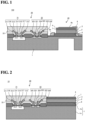
- a surface oxide film (SiO 2 film) 1b such as a thermal oxide film or a CVD (Chemical Vapor Deposition) oxide film may be formed except in the area where the semiconductor element 30 is formed. That is, the substrate 1 may be a p-type single crystal Si substrate 1a having a surface oxide film 1b.
- the thickness of the surface oxide film 1b can be, for example, 1 nm or more and 4000 nm or less.
- the substrate 1 may have an insulating film composed of an insulating material other than SiO 2 , instead of the surface oxide film 1b. Further, the substrate 1 does not need to have the surface oxide film 1b or the insulating film.
- the device 100 including the semiconductor element 30 and the piezoelectric element 20 is obtained by processing the stack 10.
- the piezoelectric element 20 is configured to include the bottom electrode film 2, the KNN film 3, and the top electrode film 4. It can be considered that the substrate 1 is included in the piezoelectric element 20.
- the bottom electrode film 2 is formed at a location on the surface of the substrate 1 on which the semiconductor element 30 is formed, which is different from the location where the semiconductor element 30 is formed.
- the piezoelectric element 20 is formed on the surface of the substrate 1 at a location different from the location where the semiconductor element 30 is formed.
- the piezoelectric element 20 further includes an insulating film 8 and metal wirings 9a and 9b.
- the metal wiring 9a is provided so as to be connected (in contact) with the bottom electrode film 2 but not connected (in contact) with the top electrode film 4. Further, the metal wiring 9b is provided so as to be connected to the top electrode film 4 and not connected to the bottom electrode film 2.
- the metal wirings 9a and 9b each can be formed using various metals such as Au, Al, Ti, Cr, etc., or alloys mainly composed of these metals.
- the metal wirings 9a and 9b may be a single layer film or a stack in which multiple layers are stacked.
- the metal wirings 9a and 9b can be formed by a technique such as a sputtering method, an evaporation method, a plating method, or a metal paste method.
- the insulating film 8 is provided to insulate the metal wiring 9b from the bottom electrode film 2.
- the insulating film 8 is provided extending from the top electrode film 4 to the substrate 1 so as to cover a part of the side surface of the KNN film 3.
- the insulating film 8 can be formed using oxide, etc., such as silicon oxide (SiO 2 ), aluminum oxide (Al 2 O 3 ), or tantalum oxide (Ta 2 O 5 ).
- the insulating film 8 may be a single layer film or a stack in which multiple layers are stacked.
- the insulating film 8 can be formed by a technique such as a CVD method or a sputtering method.
- the piezoelectric element 20 and the semiconductor element 30 are electrically connected via metal wirings 9a and 9b, and the piezoelectric element 20 is controlled by the semiconductor element 30.
- the (deforming) action of the piezoelectric element 20 is controlled by the semiconductor element 30.
- the semiconductor element 30 applies voltage between the bottom electrode film 2 and the top electrode film 4 by the semiconductor element 30 .
- deform the KNN film 3 of the piezoelectric element 20 Due to such a deforming action of the piezoelectric element 20 (KNN film 3), various structures connected to the device 100 can be operated.
- the device 100 can be applied to heads for inkjet printers, MEMS mirrors for scanners, and vibrators for ultrasonic generators, etc.
- the piezoelectric element 20 functions as a sensor
- the signal detected by the piezoelectric element 20 is processed by the semiconductor element 30.
- the KNN film 3 of the piezoelectric element 20 is deformed in accordance with a change in some physical quantity, voltage is generated between the bottom electrode film 2 and the top electrode film 4 due to the deformation. This voltage is detected as a signal by the piezoelectric element 20, and the signal detected by the piezoelectric element 20 is processed by the semiconductor element 30.
- the magnitude of the physical quantity applied to the KNN film 3 can be measured.
- the device 100 can be applied to an angular velocity sensor, an ultrasonic sensor, a pressure sensor, an acceleration sensor, etc.
- the semiconductor element 30 is operated by the electrical energy generated by the piezoelectric element 20.
- this embodiment shows that in the process of fabricating the device 100 (the stack 10), the KNN film 3 is deposited under conditions of low temperature, high oxygen partial pressure, and low atmospheric pressure.
- the stack 10 and therefore the device 100 in this embodiment can have at least one of Feature 1, Feature 2, and Feature 3 described below.
- Feature 1, Feature 2, and Feature 3 described below.
- alkali metals may diffuse and reach the substrate 1 through the bottom electrode film 2 (and the bottom adhesive layer 6).
- the adhesion between the substrate 1 and the bottom electrode film 2 (or a bottom adhesive layer 6, if present) may decrease.
- an excessively external force is repeatedly applied to the periphery (peripheral members) of the bottom electrode film 2 due to repeated large deformation of the KNN film 3 during drive of the device 100 (the piezoelectric element 20), peeling of the bottom electrode film 2 and therefore the KNN film 3 from the substrate 1 may occur.
- the KNN film 3 is deposited at a low temperature in the process of fabricating the device 100. This successfully suppresses the diffusion of alkali metals to the substrate 1 and reaching the substrate 1.
- the device 100 in this embodiment has a feature (Feature 1) such that analysis for the surface region of the substrate by secondary ion mass spectrometry (SIMS) reveals that a potassium concentration (K concentration) is 5E15 cm -3 or less and a sodium concentration (Na concentration) is 5E15 cm -3 or less.
- SIMS secondary ion mass spectrometry
- the K concentration and the Na concentration in the surface region of the substrate 1 are each 3E14 cm -3 or less. This enables to more improve the above-described adhesion. Further, it is more preferable that the K concentration in the surface region of the substrate 1 is, for example, 1E14 cm -3 or less. This enables to further improve the above-described adhesion.
- the KNN film 3 When the KNN film 3 is deposited at a low temperature, the diffusion of the alkali metals to the substrate 1 and reaching the substrate 1 can be suppressed, but the (001) orientation rate of the KNN film 3 may decrease in some cases. As a result, the performance of the piezoelectric element 20 may be degraded.
- the KNN film 3 is deposited under conditions of low temperature, high oxygen partial pressure, and low atmospheric pressure in the process of fabricating the device 100. That is, the deposition conditions for the KNN film 3 are not only low temperature but also high oxygen partial pressure and low atmospheric pressure. This enables to successfully obtain the KNN film 3 having a high (001) orientation rate (high crystal orientation) even when the KNN film 3 is deposited at a low temperature. This is a novel knowledge that was first found as a result of extensive research by the present inventors.
- the device 100 may have a feature (Feature 2) such that the (001) orientation rate of the KNN film 3 is, for example, 96 % or more, preferably 98 % or more.
- the piezoelectric element 20 Due to 96 % or more of the (001) orientation rate of the KNN film 3, the piezoelectric element 20 can have a high performance. Due to 98 % or more of the (001) orientation rate of the KNN film 3, the piezoelectric element 20 can have an even higher performance.
- the (001) orientation rate of the KNN film 3 is the orientation rate of the crystals constituting the KNN film 3 in the (001) direction.
- the (001) orientation rate of the KNN film 3 is 96 % or more” means that, for example, 96 % or more of the crystals constituting the KNN film 3 are oriented in the (001) direction with respect to the main surface of the substrate 1.
- the "orientation rate” in this specification is a value calculated from the following formula (1) based on the peak intensity in the X-ray diffraction pattern (2 ⁇ / ⁇ ) obtained by performing XRD measurement for the KNN film 3.
- Orientation rate (%) ⁇ (001) peak intensity/((001) peak intensity+(110) peak intensity) ⁇ 100
- the "(110) peak intensity" in the above formula (1) refers to, in the X-ray diffraction pattern obtained by performing XRD measurement for the KNN film 3, the intensity of a diffraction peak resulting from crystals oriented in the (110) direction (i.e., crystals whose (110) is parallel to the main surface of the substrate 1) among the crystals constituting the KNN film 3, which is the peak intensity appearing within the range of 20 of 30° to 33°, and which is the highest peak intensity when multiple peaks appear within the range of 20 of 30° to 33°.
- the KNN film 3 is required to have a perovskite structure. This is because, when the KNN film 3 does not have a perovskite structure, no peak can be observed within the range of 20 of at least 20° to 23° in the X-ray diffraction pattern obtained by performing the XRD measurement, and as a result, the (001) orientation rate cannot be calculated.
- the KNN film 3 is deposited under conditions of low temperature, high oxygen partial pressure, and low atmospheric pressure. This enables to successfully obtain the KNN film 3 having a high (001) orientation rate even when the film is deposited at a low temperature. As a result, the KNN film 3 with a high piezoelectric constant can also be obtained.
- CMOS structure formed using these techniques is vulnerable to heat. For example, when the n-type region or the p-type region is heated, the dopant may migrate, resulting in the change in the dopant concentration.
- the conditions for depositing the ZnO layer as the bottom adhesive layer 6 are exemplified as follows.
- the deposition time for the bottom adhesive layer 6 is appropriately adjusted depending on the target thickness of the bottom adhesive layer 6.
- substrate temperature refers to the surface temperature of the substrate 1 during the deposition of each film (each layer).
- the other conditions can be similar to those used when providing the ZnO layer.
- the conditions for depositing the Pt film as the bottom electrode film 2 are exemplified as follows.
- the deposition time for the bottom electrode film 2 is appropriately adjusted depending on the target thickness of the bottom electrode film 2.
- the KNN film 3 is then deposited on the bottom electrode film 2 by a sputtering method such as RF magnetron sputtering.
- the composition of the KNN film 3 can be adjusted, for example, by controlling the composition of a target used during sputtering deposition.
- the target can be fabricated by mixing K 2 CO 3 powder, Na 2 CO 3 powder, Nb 2 O 5 powder, etc., and sintering the mixture.
- the composition of the target can be controlled by adjusting the mixing ratio of K 2 CO 3 powder, Na 2 CO 3 powder, Nb 2 O 5 powder, etc.
- the deposition conditions for the KNN film 3 are a low temperature, a high oxygen partial pressure, and a low atmospheric pressure. Specifically, the conditions for depositing the KNN film 3 are exemplified as follows. The deposition time for the KNN film 3 is appropriately adjusted depending on the target thickness of the KNN film 3.
- the KNN film 3 under the above-described conditions, particularly by depositing the KNN film 3 at a depositing temperature within the range of the above-described specified conditions, the diffusion of the alkali metals to the substrate 1 and reaching the substrate 1 can be suppressed.
- the K concentration and the Na concentration in the surface region of the substrate 1 can each be 5E15 cm -3 or less. That is, the stack 10 and therefore the device 100 having the above-described Feature 1 can be obtained.
- the (001) orientation rate of the KNN film 3 can be increased to 96 % or more. That is, the stack 10 and therefore the device 100 having the above-described Feature 2 can be obtained.
- the depositing temperature of the KNN film 3 is 500 °C or more
- the thermal history of the semiconductor element 30 cannot be reduced, and as a result, shortening of the life span and degradation of the performance of the semiconductor element 30 may not be suppressed.
- the depositing temperature of the KNN film 3 is 500 °C or more
- the diffusion of the alkali metals to the substrate 1 and reaching the substrate 1 may not be suppressed.
- the thermal history of the semiconductor element 30 can be reduced. Thereby, for example, migration of dopants in the n-type region and p-type region of the semiconductor element 30 can be suppressed. As a result, shortening of the life span and degradation of the performance of the semiconductor element 30 can be suppressed. Further, the manufacturing yield of the device 100 can be increased. Further, due to the depositing temperature of the KNN film 3 being less than 500 °C, the diffusion of the alkali metals can be suppressed, and the K concentration and the Na concentration each in the surface region of the substrate 1 can be reduced. As a result, the K concentration and the Na concentration in the surface region of the substrate 1 can each be reduced to 5E15 cm -3 or less.
- the thermal history of the semiconductor element 30 can be further reduced. Further, the diffusion of the alkali metals can be reliably suppressed, and the K concentration and the Na concentration in the surface region of the substrate 1 can be further reduced.
- the K concentration and the Na concentration in the surface region of the substrate 1 can each be 3E14 cm -3 or less, and further, the K concentration in the surface region of the substrate 1 can be 1E14 cm -3 or less.
- the (001) orientation rate of the KNN film 3 may decrease, while saturating the effect of suppressing the diffusion of the alkali metals to the substrate 1 and reaching the substrate 1.
- the (001) orientation rate of the KNN film 3 may not be increased to 96 % or more. Therefore, the absolute value of the piezoelectric constant e 31 may not be increased to 7 C/m 2 or more. As a result of these, the performance of the piezoelectric element 20 may be degraded.
- the (001) orientation rate of the KNN film 3 can be increased to 96 % or more and the absolute value of the piezoelectric constant e 31 can be increased to 7 C/m 2 or more, while suppressing the diffusion of alkali metals to the substrate 1 and reaching the substrate 1.
- the stack 10 and therefore the device 100 in which the semiconductor element 30 and the high-performance piezoelectric element 20 are formed on the same substrate 1, can be obtained.
- the (001) orientation rate of the KNN film 3 may not be increased sufficiently. That is, when the depositing temperature of the KNN film 3 is 400 °C or more and less than 500 °C and when the oxygen partial pressure is less than 0.0025 Pa, the (001) orientation rate of the KNN film 3 may not be increased to 96 % or more. Therefore, the absolute value of the piezoelectric constant e 31 may not be increased to 7 C/m 2 or more. As a result of these, the performance of the piezoelectric element 20 may be degraded.
- the oxygen partial pressure being less than 0.01 Pa
- the decrease in the (001) orientation rate of the KNN film 3 can be suppressed, and even when the depositing temperature of the KNN film 3 is 400 °C or more and less than 500 °C, the (001) orientation rate of the KNN film 3 can be increased to 96 % or more, and the absolute value of the piezoelectric constant e 31 of the KNN film 3 can be increased to 7 C/m 2 or more.
- the stack 10 and therefore the device 100 in which the semiconductor element 30 and the high-performance piezoelectric element 20 are formed on the same substrate 1, can be obtained.
- the (001) orientation rate of the KNN film 3 may not be increased sufficiently. Accordingly, when the depositing temperature of the KNN film 3 is 400 °C or more and less than 500 °C and when the atmospheric pressure is 0.1 Pa or more, the (001) orientation rate of the KNN film 3 may not be increased to 96 % or more. Therefore, the absolute value of the piezoelectric constant e 31 may not be increased to 7 C/m 2 or more. As a result of these, the performance of the piezoelectric element 20 may be degraded.
- the (001) orientation rate of the KNN film 3 can be sufficiently increased, and even when the depositing temperature of the KNN film 3 is 400 °C or more and less than 500 °C, the (001) orientation rate of the KNN film 3 can be increased to 96 % or more, and the absolute value of the piezoelectric constant e 31 of the KNN film 3 can be increased to 7 C/m 2 or more.
- the stack 10 and therefore the device 100 in which the semiconductor element 30 and the high-performance piezoelectric element 20 are formed on the same substrate 1, can be obtained.
- the (001) orientation rate of the KNN film 3 may not be increased sufficiently. Accordingly, when the depositing temperature of the KNN film 3 is 400 °C or more and less than 500 °C and when the atmospheric pressure is less than 0.03 Pa, the (001) orientation rate of the KNN film 3 may not be increased to 96 % or more. Therefore, the absolute value of the piezoelectric constant e 31 may not be increased to 7 C/m 2 or more. As a result of these, the performance of the piezoelectric element 20 may be degraded.
- the (001) orientation rate of the KNN film 3 can be sufficiently increased, and even when the depositing temperature of the KNN film 3 is 400 °C or more and less than 500 °C, the (001) orientation rate of the KNN film 3 can be increased to 96 % or more, and the absolute value of the piezoelectric constant e 31 of the KNN film 3 can be increased to 7 C/m 2 or more.
- the stack 10 and therefore the device 100 in which the semiconductor element 30 and the high-performance piezoelectric element 20 are formed on the same substrate 1, can be obtained.
- the device 100 (stack 10) in which the semiconductor element 30 and the piezoelectric element 20 are formed on the same substrate 1 can be obtained while reducing the thermal history of the semiconductor element 30. Further, while reducing the thermal history of the semiconductor element 30, the device 100 (stack 10) having at least one of the above-described Features 1, 2, and 3, preferably all of the above-described Features 1, 2, and 3, can be obtained. That is, the stack 10 and therefore the device 100 in which the semiconductor element 30 and the high-performance piezoelectric element 20 are formed on the same substrate 1, can be obtained.
- the top adhesive layer 7 e.g., a RuO 2 layer
- the top electrode film 4 e.g., a Pt film
- the conditions for depositing the RuO 2 layer, etc., as the top adhesive layer 7 are exemplified as follows.
- the deposition time for the top adhesive layer 7 is appropriately adjusted depending on the target thickness of the top adhesive layer 7.
- the conditions for depositing the Pt film, etc., as the top electrode film 4 are exemplified as follows.
- the deposition time for the top electrode film 4 is appropriately adjusted depending on the target thickness of the top electrode film 4.
- the device 100 (stack 10) having at least one of the above-described Features 1, 2, and 3, preferably all of the above-described Features 1, 2, and 3, can be obtained while reducing the thermal history of the semiconductor element 30.
- the bottom adhesive layer 6, the bottom electrode film 2, the KNN film 3, the top adhesive layer 7, and the top electrode film 4 are deposited in this order. Thereby, the stack 10 as shown in FIG. 2 can be obtained.
- the stack 10 is processed to form a piezoelectric element 20 on the substrate 1.
- the top electrode film 4 (including the top adhesive layer 7) and the KNN film 3 are individually patterned by dry etching using Ar gas or reactive gas.
- the top electrode film 4 (including the top adhesive layer 7) and the KNN film 3 are each formed into a predetermined shape, and a part of the bottom electrode film 2 is exposed.
- a photoresist can be used as an etching mask.
- an insulating film 8 and metal wirings 9a and 9b are provided. Specifically, first, a layer composed of an insulating material (that is, the insulating film 8) is provided extending from the top electrode film 4 to the substrate 1 so as to cover the side surface of the KNN film 3 by a technique such as a CVD method or sputtering method. Then, the insulating film 8 is patterned by dry etching using Ar gas or reactive gas such as CF 4 gas, or wet etching, to form the insulating film 8 into a predetermined shape.
- a layer composed of an insulating material that is, the insulating film 8
- Ar gas or reactive gas such as CF 4 gas
- a layer composed of a material containing metal is provided by a technique such as a sputtering method, evaporation method, plating method, or metal paste method. Then, the metal wiring layer is patterned by dry etching using Ar gas or reactive gas, or wet etching, to thereby form metal wirings 9a and 9b.
- the metal wiring 9a is formed (patterned) so as to be connected to the bottom electrode film 2 and not connected to the top electrode film 4, and the metal wiring 9b is formed so as to be connected to the top electrode film 4 and not connected to the bottom electrode film.
- the etching conditions for patterning when forming the insulating film 8 and the metal wirings 9a and 9b, and the etching conditions for the substrate 1 when processing the piezoelectric stack 10 into the piezoelectric element 20, can be general etching conditions used in a semiconductor device manufacturing process, as long as the insulation properties of the KNN film 3 are not deteriorated.
- the piezoelectric element 20 is formed on the substrate 1.
- the device 100 in which the piezoelectric element 20 and the semiconductor element 30 are formed on the same substrate 1 as shown in FIG. 1 can be obtained.
- a bonding technique that is a technique of depositing a first electrode film, a KNN film, and a second electrode film on a first substrate in this order, bonding a second substrate on which a semiconductor element 30 is previously formed, to the top surface of the second electrode film, and then, removing the first substrate, to thereby fabricate a piezoelectric stack. It is considered that in the piezoelectric stack fabricated by using such a bonding technique, the thermal history of the semiconductor element 30 is reduced, and alkali metals don't diffuse to the second substrate and don't reach the second substrate.
- the stack 10 in which the semiconductor element 30 and the piezoelectric element 20 are formed on the same substrate 1 is fabricated without using the bonding technique, and further, in the fabrication process, the diffusion of alkali metals to the substrate 1 and reaching the substrate 1 is suppressed while reducing the thermal history of the semiconductor element 30.
- the adhesion between the substrate 1 and the bottom electrode film 2 (bottom adhesive layer 6) is successfully improved, while reducing the thermal history of the semiconductor element 30.
- the stack 10 since the stack 10 is fabricated without using the bonding technique, the stack 10 (the piezoelectric element 20) according to this embodiment has no traces resulting from bonding.
- the "traces resulting from bonding" are as follows: the presence (distribution) of inclusions (e.g., adhesive) used in bonding, and the presence (distribution) of impurities not resulting from the deposition process (e.g., impurities resulting from the adhesive).
- the piezoelectric element 20 may be formed on the semiconductor element 30.
- the "surface region of the substrate 1" is the region extending from the interface between the piezoelectric element 20 and the semiconductor element 30 (or protective film 33, if the protective film 33 is provided) to a depth of 1 ⁇ m toward the rear surface of substrate 1.
- the piezoelectric element 20 may be formed on the top surface of the substrate 1 such that a portion of the piezoelectric element 20 is located above the semiconductor element 30.
- the "surface region of the substrate 1" is the region extending from the interface between the piezoelectric element 20 and the semiconductor element 30 (protective film 33) or the substrate 1 to a depth of 1 ⁇ m toward the rear surface of the substrate 1.
- the thermal history of the semiconductor element 30 can be reduced.
- the stack 10 and therefore the device 100 in which the semiconductor element 30 and the piezoelectric element 20 are formed on the same substrate 1 can be obtained.
- the stack 10 and therefore the device 100 may have at least one of the above-described Features 1, 2, and 3.
- the above embodiment shows the case in which the substrate 1 is a p-type single crystal Si substrate 1a, that is, the substrate 1 is a p-type semiconductor substrate, but the present disclosure is not limited thereto.
- the substrate 1 may be an n-type semiconductor substrate.
- the p-type MOSFET 31 does not include the n-well 311, and the p-type source region 312 and the p-type drain region 313 are provided spaced apart from each other on the top surface of the substrate 1. Further, the n-type source region 321 and the n-type drain region 322 of the n-type MOSFET 32 are provided spaced apart from each other in a p-well formed on the top surface of the substrate 1.
- the thermal history of the semiconductor element 30 can be reduced.
- the stack 10 and therefore the device 100 in which the semiconductor element 30 and the piezoelectric element 20 are formed on the same substrate 1 can be obtained.
- the stack 10 and therefore the device 100 may have at least one of the above-described Features 1, 2, and 3.
- the semiconductor element 30 has a CMOS structure.
- the semiconductor element 30 is not limited to CMOS, so long as it has an element structure that is vulnerable to heat.
- An element formed by using a technique of thermal diffusion or ion implantation of dopants to form the n-type or p-type region is vulnerable to heat. Accordingly, when the semiconductor element 30 is formed using these techniques, that is, when the semiconductor element 30 has a region in which the p-type or n-type dopants are thermally diffused or a region in which the dopants are ion-implanted, this embodiment can be suitably applied, and similar effects to the above-described embodiments and variations can be obtained.
- the KNN film 3 is deposited at a low temperature of 400 °C or more and less than 500 °C, other substrate for which a small thermal history is required, can be used as the substrate 1.
- the substrate 1 the substrate on which a CMUT (Capacitive Micro-machined Ultrasound Transducer) structure is formed can be used.
- CMUT Capacitive Micro-machined Ultrasound Transducer
- a resin substrate or a glass substrate which is vulnerable to heat can also be used as the substrate 1.
- a high-performance piezoelectric element 20 can be formed on the substrate 1 that is required to have a small thermal history or on the substrate 1 that is vulnerable to heat.
- the stack 10 and therefore the device 100 can have at least one of the above-described Features 1, 2, and 3.
- the stack 10 and therefore the device 100 may have at least one of the above-described Features 1, 2, and 3.
- the above-described embodiments and variations show the case in which the bottom adhesive layer 6 and the bottom electrode film 2 are provided, but the present disclosure is not limited thereto.
- the bottom adhesive layer 6 and the bottom electrode film 2 may not be provided. That is, the KNN film 3 may be deposited directly on the substrate 1.
- the piezoelectric element 20 is configured to include at least the KNN film 3 and the top electrode film 4 (including the top adhesive layer 7).
- the substrate 1 can be any of the substrates described in the above-described variations 1 to 4.
- the semiconductor element 30 and the piezoelectric element 20 can be formed on the same substrate 1.
- the stack 10 and therefore the device 100 may have at least one of the above-described Features 1, 2, and 3.
- the piezoelectric element is controlled by the semiconductor element.
Landscapes
- Engineering & Computer Science (AREA)
- Chemical & Material Sciences (AREA)
- Materials Engineering (AREA)
- Ceramic Engineering (AREA)
- Manufacturing & Machinery (AREA)
- Physical Vapour Deposition (AREA)
- Inorganic Compounds Of Heavy Metals (AREA)
- Surface Acoustic Wave Elements And Circuit Networks Thereof (AREA)
Applications Claiming Priority (1)
| Application Number | Priority Date | Filing Date | Title |
|---|---|---|---|
| JP2023220952A JP2025103514A (ja) | 2023-12-27 | 2023-12-27 | 圧電素子を備える装置、積層基板、及びその装置の製造方法 |
Publications (1)
| Publication Number | Publication Date |
|---|---|
| EP4580382A1 true EP4580382A1 (de) | 2025-07-02 |
Family
ID=93743808
Family Applications (1)
| Application Number | Title | Priority Date | Filing Date |
|---|---|---|---|
| EP24216851.6A Pending EP4580382A1 (de) | 2023-12-27 | 2024-12-02 | Vorrichtung mit piezoelektrischem element und verfahren zur herstellung der vorrichtung |
Country Status (5)
| Country | Link |
|---|---|
| US (1) | US20250221316A1 (de) |
| EP (1) | EP4580382A1 (de) |
| JP (1) | JP2025103514A (de) |
| CN (1) | CN120225032A (de) |
| TW (1) | TW202545381A (de) |
Citations (8)
| Publication number | Priority date | Publication date | Assignee | Title |
|---|---|---|---|---|
| JP2007184513A (ja) | 2005-12-06 | 2007-07-19 | Seiko Epson Corp | 圧電体積層体、表面弾性波素子、薄膜圧電共振子および圧電アクチュエータ |
| JP2008159807A (ja) | 2006-12-22 | 2008-07-10 | Hitachi Cable Ltd | 圧電薄膜素子及び圧電薄膜素子を用いて製造したアクチュエータとセンサ |
| US7732996B2 (en) * | 2008-01-24 | 2010-06-08 | Hitachi Cable, Ltd. | Piezoelectric thin film device |
| US20180287048A1 (en) * | 2017-03-28 | 2018-10-04 | Seiko Epson Corporation | Piezoelectric Element And Piezoelectric Element-Applied Device |
| WO2019139100A1 (ja) * | 2018-01-10 | 2019-07-18 | 国立大学法人東京工業大学 | 圧電体膜の製造方法 |
| WO2022224594A1 (ja) * | 2021-04-20 | 2022-10-27 | 住友化学株式会社 | 圧電積層体、圧電積層体の製造方法、スパッタリングターゲット材、及びスパッタリングターゲット材の製造方法 |
| US20230142065A1 (en) * | 2020-04-06 | 2023-05-11 | Sumitomo Chemical Company, Limited | Piezoelectric laminate, production method for piezoelectric laminate, and piezoelectric element |
| WO2024202319A1 (ja) * | 2023-03-29 | 2024-10-03 | 住友化学株式会社 | 圧電積層体、圧電積層体の製造方法、及び圧電素子 |
-
2023
- 2023-12-27 JP JP2023220952A patent/JP2025103514A/ja active Pending
-
2024
- 2024-10-18 TW TW113139669A patent/TW202545381A/zh unknown
- 2024-12-02 EP EP24216851.6A patent/EP4580382A1/de active Pending
- 2024-12-23 US US18/999,260 patent/US20250221316A1/en active Pending
- 2024-12-24 CN CN202411909785.4A patent/CN120225032A/zh active Pending
Patent Citations (8)
| Publication number | Priority date | Publication date | Assignee | Title |
|---|---|---|---|---|
| JP2007184513A (ja) | 2005-12-06 | 2007-07-19 | Seiko Epson Corp | 圧電体積層体、表面弾性波素子、薄膜圧電共振子および圧電アクチュエータ |
| JP2008159807A (ja) | 2006-12-22 | 2008-07-10 | Hitachi Cable Ltd | 圧電薄膜素子及び圧電薄膜素子を用いて製造したアクチュエータとセンサ |
| US7732996B2 (en) * | 2008-01-24 | 2010-06-08 | Hitachi Cable, Ltd. | Piezoelectric thin film device |
| US20180287048A1 (en) * | 2017-03-28 | 2018-10-04 | Seiko Epson Corporation | Piezoelectric Element And Piezoelectric Element-Applied Device |
| WO2019139100A1 (ja) * | 2018-01-10 | 2019-07-18 | 国立大学法人東京工業大学 | 圧電体膜の製造方法 |
| US20230142065A1 (en) * | 2020-04-06 | 2023-05-11 | Sumitomo Chemical Company, Limited | Piezoelectric laminate, production method for piezoelectric laminate, and piezoelectric element |
| WO2022224594A1 (ja) * | 2021-04-20 | 2022-10-27 | 住友化学株式会社 | 圧電積層体、圧電積層体の製造方法、スパッタリングターゲット材、及びスパッタリングターゲット材の製造方法 |
| WO2024202319A1 (ja) * | 2023-03-29 | 2024-10-03 | 住友化学株式会社 | 圧電積層体、圧電積層体の製造方法、及び圧電素子 |
Also Published As
| Publication number | Publication date |
|---|---|
| TW202545381A (zh) | 2025-11-16 |
| JP2025103514A (ja) | 2025-07-09 |
| US20250221316A1 (en) | 2025-07-03 |
| CN120225032A (zh) | 2025-06-27 |
Similar Documents
| Publication | Publication Date | Title |
|---|---|---|
| EP3922749B1 (de) | Sputtertarget zur herstellung piezoelektrischer dünnschichten sowie verfahren zur herstellung des sputtertargets | |
| EP2187462B1 (de) | Piezoelektrische/elektrostriktive keramische Zusammensetzung, piezoelektrischer/elektrostriktiver keramischer gesinterteter Körper, Herstellungsverfahren einer piezoelektrischen/elektrostriktiven keramischen Zusammensetzung, Herstellungsverfahren eines piezoelektrischen/elektrostriktiven keramischen Elementes | |
| EP3772114B1 (de) | Piezoelektrisches bauelement und herstellungsverfahren dafür | |
| JP2013080887A (ja) | 圧電体素子及びその製造方法、並びに液体吐出ヘッド | |
| EP3540797B1 (de) | Piezoelektrisches laminat, verfahren zur herstellung des piezoelektrischen laminats und piezoelektrisches element | |
| US12501832B2 (en) | Piezoelectric thin film, piezoelectric thin film element, and piezoelectric transducer | |
| CN104944942B (zh) | 压电组合物和压电元件 | |
| EP3985747B1 (de) | Piezoelektrisches element | |
| US20050146772A1 (en) | Piezoelectric element, method for fabricating the same, inkjet head, method for fabricating the same, and inkjet recording apparatus | |
| US9705070B2 (en) | Ferroelectric thin film, method of manufacturing same and method of manufacturing piezoelectric element | |
| CN104628380B (zh) | 压电组合物和压电元件 | |
| JPH05270912A (ja) | 圧電/電歪膜型素子 | |
| EP4580382A1 (de) | Vorrichtung mit piezoelektrischem element und verfahren zur herstellung der vorrichtung | |
| CN104817320B (zh) | 压电组合物和压电元件 | |
| EP4580381A1 (de) | Gestapeltes substrat mit piezoelektrischem film, verfahren zur herstellung des gestapelten substrats und piezoelektrisches element | |
| JP7667051B2 (ja) | 圧電積層体及び圧電素子 | |
| JP7490796B2 (ja) | 圧電素子 | |
| US20240206342A1 (en) | Piezoelectric film, piezoelectric stack, piezoelectric element, and method for producing piezoelectric stack | |
| EP4686370A1 (de) | Piezoelektrischer stapel und verfahren zur herstellung des piezoelektrischen stapels | |
| EP4686371A1 (de) | Piezoelektrischer mehrschichtkörper, piezoelektrischer mehrschichtwafer und verfahren zur herstellung eines piezoelektrischen mehrschichtkörpers | |
| US20260033243A1 (en) | Piezoelectric stack and method for manufacturing the piezoelectric stack | |
| JPH11348277A (ja) | インクジェットプリンタヘッド | |
| EP3276687B1 (de) | Ferroelektrisches dünnschichtlaminatsubstrat, ferroelektrisches dünnschichtelement und herstellungsverfahren für ein ferroelektrisches dünnschichtlaminatsubstrat | |
| EP4178333B1 (de) | Piezoelektrisches laminat, piezoelektrisches element und herstellungsverfahren für piezoelektrisches laminat | |
| US20240023454A1 (en) | Piezoelectric element and manufacturing method for piezoelectric element |
Legal Events
| Date | Code | Title | Description |
|---|---|---|---|
| PUAI | Public reference made under article 153(3) epc to a published international application that has entered the european phase |
Free format text: ORIGINAL CODE: 0009012 |
|
| STAA | Information on the status of an ep patent application or granted ep patent |
Free format text: STATUS: THE APPLICATION HAS BEEN PUBLISHED |
|
| AK | Designated contracting states |
Kind code of ref document: A1 Designated state(s): AL AT BE BG CH CY CZ DE DK EE ES FI FR GB GR HR HU IE IS IT LI LT LU LV MC ME MK MT NL NO PL PT RO RS SE SI SK SM TR |
|
| STAA | Information on the status of an ep patent application or granted ep patent |
Free format text: STATUS: REQUEST FOR EXAMINATION WAS MADE |
|
| 17P | Request for examination filed |
Effective date: 20251128 |