EP4580368A2 - Anzeigevorrichtung - Google Patents
Anzeigevorrichtung Download PDFInfo
- Publication number
- EP4580368A2 EP4580368A2 EP24206136.4A EP24206136A EP4580368A2 EP 4580368 A2 EP4580368 A2 EP 4580368A2 EP 24206136 A EP24206136 A EP 24206136A EP 4580368 A2 EP4580368 A2 EP 4580368A2
- Authority
- EP
- European Patent Office
- Prior art keywords
- layer
- trench
- sloped surface
- electrode
- light emitting
- Prior art date
- Legal status (The legal status is an assumption and is not a legal conclusion. Google has not performed a legal analysis and makes no representation as to the accuracy of the status listed.)
- Pending
Links
Images











Classifications
-
- H—ELECTRICITY
- H10—SEMICONDUCTOR DEVICES; ELECTRIC SOLID-STATE DEVICES NOT OTHERWISE PROVIDED FOR
- H10K—ORGANIC ELECTRIC SOLID-STATE DEVICES
- H10K59/00—Integrated devices, or assemblies of multiple devices, comprising at least one organic light-emitting element covered by group H10K50/00
- H10K59/10—OLED displays
- H10K59/12—Active-matrix OLED [AMOLED] displays
- H10K59/124—Insulating layers formed between TFT elements and OLED elements
-
- H—ELECTRICITY
- H10—SEMICONDUCTOR DEVICES; ELECTRIC SOLID-STATE DEVICES NOT OTHERWISE PROVIDED FOR
- H10K—ORGANIC ELECTRIC SOLID-STATE DEVICES
- H10K59/00—Integrated devices, or assemblies of multiple devices, comprising at least one organic light-emitting element covered by group H10K50/00
- H10K59/80—Constructional details
- H10K59/87—Passivation; Containers; Encapsulations
- H10K59/873—Encapsulations
- H10K59/8731—Encapsulations multilayered coatings having a repetitive structure, e.g. having multiple organic-inorganic bilayers
-
- H—ELECTRICITY
- H10—SEMICONDUCTOR DEVICES; ELECTRIC SOLID-STATE DEVICES NOT OTHERWISE PROVIDED FOR
- H10K—ORGANIC ELECTRIC SOLID-STATE DEVICES
- H10K59/00—Integrated devices, or assemblies of multiple devices, comprising at least one organic light-emitting element covered by group H10K50/00
- H10K59/10—OLED displays
- H10K59/12—Active-matrix OLED [AMOLED] displays
- H10K59/131—Interconnections, e.g. wiring lines or terminals
-
- H—ELECTRICITY
- H10—SEMICONDUCTOR DEVICES; ELECTRIC SOLID-STATE DEVICES NOT OTHERWISE PROVIDED FOR
- H10K—ORGANIC ELECTRIC SOLID-STATE DEVICES
- H10K50/00—Organic light-emitting devices
- H10K50/80—Constructional details
- H10K50/84—Passivation; Containers; Encapsulations
-
- H—ELECTRICITY
- H10—SEMICONDUCTOR DEVICES; ELECTRIC SOLID-STATE DEVICES NOT OTHERWISE PROVIDED FOR
- H10K—ORGANIC ELECTRIC SOLID-STATE DEVICES
- H10K50/00—Organic light-emitting devices
- H10K50/80—Constructional details
- H10K50/84—Passivation; Containers; Encapsulations
- H10K50/844—Encapsulations
-
- H—ELECTRICITY
- H10—SEMICONDUCTOR DEVICES; ELECTRIC SOLID-STATE DEVICES NOT OTHERWISE PROVIDED FOR
- H10K—ORGANIC ELECTRIC SOLID-STATE DEVICES
- H10K59/00—Integrated devices, or assemblies of multiple devices, comprising at least one organic light-emitting element covered by group H10K50/00
- H10K59/30—Devices specially adapted for multicolour light emission
- H10K59/38—Devices specially adapted for multicolour light emission comprising colour filters or colour changing media [CCM]
-
- H—ELECTRICITY
- H10—SEMICONDUCTOR DEVICES; ELECTRIC SOLID-STATE DEVICES NOT OTHERWISE PROVIDED FOR
- H10K—ORGANIC ELECTRIC SOLID-STATE DEVICES
- H10K59/00—Integrated devices, or assemblies of multiple devices, comprising at least one organic light-emitting element covered by group H10K50/00
- H10K59/80—Constructional details
- H10K59/805—Electrodes
- H10K59/8052—Cathodes
- H10K59/80521—Cathodes characterised by their shape
-
- H—ELECTRICITY
- H10—SEMICONDUCTOR DEVICES; ELECTRIC SOLID-STATE DEVICES NOT OTHERWISE PROVIDED FOR
- H10K—ORGANIC ELECTRIC SOLID-STATE DEVICES
- H10K59/00—Integrated devices, or assemblies of multiple devices, comprising at least one organic light-emitting element covered by group H10K50/00
- H10K59/80—Constructional details
- H10K59/87—Passivation; Containers; Encapsulations
-
- H—ELECTRICITY
- H10—SEMICONDUCTOR DEVICES; ELECTRIC SOLID-STATE DEVICES NOT OTHERWISE PROVIDED FOR
- H10K—ORGANIC ELECTRIC SOLID-STATE DEVICES
- H10K59/00—Integrated devices, or assemblies of multiple devices, comprising at least one organic light-emitting element covered by group H10K50/00
- H10K59/80—Constructional details
- H10K59/87—Passivation; Containers; Encapsulations
- H10K59/873—Encapsulations
-
- H—ELECTRICITY
- H10—SEMICONDUCTOR DEVICES; ELECTRIC SOLID-STATE DEVICES NOT OTHERWISE PROVIDED FOR
- H10K—ORGANIC ELECTRIC SOLID-STATE DEVICES
- H10K59/00—Integrated devices, or assemblies of multiple devices, comprising at least one organic light-emitting element covered by group H10K50/00
- H10K59/80—Constructional details
- H10K59/875—Arrangements for extracting light from the devices
- H10K59/878—Arrangements for extracting light from the devices comprising reflective means
-
- H—ELECTRICITY
- H10—SEMICONDUCTOR DEVICES; ELECTRIC SOLID-STATE DEVICES NOT OTHERWISE PROVIDED FOR
- H10K—ORGANIC ELECTRIC SOLID-STATE DEVICES
- H10K50/00—Organic light-emitting devices
- H10K50/10—OLEDs or polymer light-emitting diodes [PLED]
- H10K50/19—Tandem OLEDs
-
- H—ELECTRICITY
- H10—SEMICONDUCTOR DEVICES; ELECTRIC SOLID-STATE DEVICES NOT OTHERWISE PROVIDED FOR
- H10K—ORGANIC ELECTRIC SOLID-STATE DEVICES
- H10K59/00—Integrated devices, or assemblies of multiple devices, comprising at least one organic light-emitting element covered by group H10K50/00
- H10K59/30—Devices specially adapted for multicolour light emission
- H10K59/35—Devices specially adapted for multicolour light emission comprising red-green-blue [RGB] subpixels
- H10K59/351—Devices specially adapted for multicolour light emission comprising red-green-blue [RGB] subpixels comprising more than three subpixels, e.g. red-green-blue-white [RGBW]
Definitions
- Embodiments of the present disclosure relate to a display device.
- LCD liquid crystal display device
- OLED organic light emitting display device
- an organic light emitting display device as a self-emissive type provides advantages in that it has a superior viewing angle and contrast ratio compared to a liquid crystal display device (LCD) and does not require a separate backlight to be lightweight and thin and be advantageous in terms of power consumption.
- the organic light emitting display device provides advantages in that it is capable of being driven at a low direct current voltage and has a fast response speed and especially a low manufacturing cost.
- embodiments of the present disclosure are directed to a display device that substantially obviates one or more of the problems due to limitations and disadvantages of the related art.
- Another aspect of the present disclosure is to provide a display device that can suppress side leakage current to prevent an unintended subpixel from emitting light and can improve color gamut and display quality at a low grayscale.
- a display device including a plurality of light emitting areas corresponding to a plurality of subpixels, comprises: a substrate; a circuit element layer on the substrate; a first passivation layer covering the circuit element layer; a first overcoat layer on the first passivation layer; a second passivation layer on the first overcoat layer, the second passivation layer having a first trench through the second passivation layer at a portion between two neighboring light emitting areas among the plurality of light emitting areas, wherein the second passivation layer includes a first sloped surface exposed by the first trench; a second overcoat layer on the second passivation layer, the second overcoat layer having a second trench defined by a second sloped surface of the second overcoat layer adjacent to the first trench, and the second trench
- a display device including a plurality of light emitting areas corresponding to a plurality of subpixels, comprises: a substrate; a circuit element layer on the substrate; a first passivation layer on the circuit element layer; a color filter layer on the first passivation layer; a second passivation layer covering the color filter layer; an overcoat layer on the second passivation layer, the overcoat layer having first trench with a first sloped surface of the overcoat layer at a portion between two neighboring light emitting areas among the plurality of light emitting areas; a first electrode on the overcoat layer and exposing the first trench; an organic layer on the first electrode and the first sloped surface; and a second electrode on the organic layer.
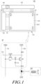
- a display device 100 includes a display panel 110.
- the display device 100 includes a driving circuit for driving various signal lines and so on disposed in the display panel 110.
- the driving circuit may include a gate driving circuit 120, a data driving circuit 130 and a controller 140.
- the display panel 110 includes an active area A/A and a non-active area N/A outside the active area A/A.
- a plurality of subpixels SP are disposed in the active area A/A of the display panel 110.
- a plurality of gate lines GL that extend in a first direction (e.g., a column direction or a row direction) and a plurality of data lines DL that extend in a second direction intersecting the first direction are disposed in the display panel 110, and the subpixels SP may be disposed in areas where the gate lines GL and the data lines DL intersect each other.
- the gate driving circuit 120 may be formed separately from the display panel 110, and may be connected to the display panel 110 in a tape automated bonding (TAB) method, may be connected to the bonding pads of the display panel 110 in a chip-on-glass (COG) or chip-on-panel (COP) method or may be connected to the display panel 110 by being implemented in a chip-on-film (COF) method.
- TAB tape automated bonding
- COG chip-on-glass
- COF chip-on-film
- the data driving circuit 130 may output data signals (also referred to as "data voltages") corresponding to image signals to the plurality of data lines DL.
- the data driving circuit 130 may include at least one source driver integrated circuit.
- each source driver integrated circuit may be connected to the display panel 110 in a tape automated bonding (TAB) method, may be connected to the bonding pads of the display panel 110 in a COG or COP method or may be connected to the display panel 110 by being implemented in a COF method.
- TAB tape automated bonding
- the subpixel SP may include a light emitting element ED and a pixel driving circuit for driving the same.
- the pixel driving circuit may include a driving transistor DRT, a scan transistor SCT and a storage capacitor Cst.
- the storage capacitor Cst may be connected between the first node N1 and the second node N2 of the driving transistor DRT, and may maintain the voltage of the second node N2 for a certain period of time.
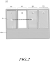
- FIG. 2 is a plan view schematically showing pixels disposed in the display panel of a display device according to embodiments of the present disclosure
- FIG. 3 is a view showing an example of a cross-section taken along the line I-I' of FIG. 2
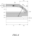
- FIG. 4 is an enlarged view of the part A of FIG. 3 .
- a plurality of subpixels SP1 to SP4 are disposed in an active area A/A of the display panel.
- the subpixels SP1 to SP4 may include a red (R) subpixel SP1, a white (W) subpixel SP2, a blue (B) subpixel SP3 and a green (G) subpixel SP4.
- R red
- W white
- B blue
- G green
- the subpixels SP1 to SP4 may be disposed in the order of the red subpixel SP1, the white subpixel SP2, the blue subpixel SP3 and the green subpixel SP4, but the disposition order of subpixels is not limited thereto and may be changed in various ways.
- an organic layer that generates white (W) light may be disposed in common in the subpixels SP1 to SP4, a red (R) color filter is disposed in the red subpixel SP1, a blue (B) color filter is disposed in the blue subpixel SP3, and a green (G) color filter is disposed in the green subpixel SP4.
- R red
- B blue
- G green
- a separate color filter is not disposed in the white subpixel SP2.
- the display panel of the display device may include a substrate 10.
- a circuit element layer 20 may be disposed on the substrate 10.
- the circuit element layer 20 may include circuit elements (e.g., driving transistors, sensing transistors and storage capacitors), which constitute subpixels, and wirings 21.
- the circuit element layer 20 may include a first conductive layer that is disposed on the substrate 10.
- the first conductive layer may include a plurality of wirings 21.
- the wirings 21 may include data lines, driving voltage lines and sensing lines.
- the wirings 21 may be disposed in the non-light emitting area NEA between neighboring light emitting areas EA.
- the first conductive layer may include a light blocking layer and a bottom electrode of each storage capacitor, which are not shown.
- the light blocking layer may be disposed to overlap the semiconductor pattern of each driving transistor to protect an oxide semiconductor element from external light.
- the bottom electrode of the storage capacitor may be electrically connected to the gate node of the driving transistor.
- the circuit element layer 20 may include a buffer layer 22.
- the buffer layer 22 may be disposed on the substrate 10 to cover the wirings 21, the light blocking layer and the bottom electrode of the storage capacitor.
- the buffer layer 22 may prevent ions or impurities from diffusing from the substrate 10 and block moisture penetration. In addition, the buffer layer 22 may improve surface flatness.
- the buffer layer 22 may include an inorganic material such as oxide or nitride, an organic material or an organic-inorganic composite, and may be formed in a single-layer or multi-layer structure.
- the buffer layer 22 may have the structure of at least a triple layer made of silicon oxide, silicon nitride and silicon oxide. In another embodiment, the buffer layer 22 may be omitted.
- the circuit element layer 20 may include an active layer, a gate insulating layer and a second conductive layer.
- the active layer may be disposed on the buffer layer 22.
- the active layer may be formed of a silicon-based semiconductor material or an oxide-based semiconductor material.
- As the silicon-based semiconductor material amorphous silicon or polycrystalline silicon may be used.
- quaternary metal oxide such as indium tin gallium zinc oxide (InSnGaZnO), ternary metal oxide such as indium gallium zinc oxide (InGaZnO), indium tin zinc oxide (InSnZnO), indium aluminum zinc oxide (InAlZnO), tin gallium zinc oxide (SnGaZnO), aluminum gallium zinc oxide (AlGaZnO) and tin aluminum zinc oxide (SnAlZnO), binary metal oxide such as indium zinc oxide (InZnO), tin zinc oxide (SnZnO), aluminum zinc oxide (AlZnO), zinc magnesium oxide (ZnMgO), tin magnesium oxide (SnMgO), indium magnesium oxide (InMgO) and indium gallium oxide (InGaO), or mono-metal oxide such as indium oxide (InO), tin oxide (SnO) and zinc oxide (ZnO) may be used.
- the active layer may include a source
- the gate insulating layer may be disposed on the active layer.
- the second conductive layer may be disposed on the gate insulating layer.
- the second conductive layer may include a gate electrode, a source electrode and a drain electrode.
- the second conductive layer may further include a top electrode of the storage capacitor.
- a first passivation layer 30 may be disposed on the circuit element layer 20.
- the first passivation layer 30 may cover the second conductive layer (not shown) and the buffer layer 22 that is not covered by the second conductive layer.
- the first passivation layer 30 may include a photosensitive organic material.
- the first passivation layer 30 may be formed as an inorganic insulating layer such as silicon nitride (SiNx) and silicon oxide (SiOx) or an organic insulating layer such as polyacrylate and polyimide, and the embodiments of the present disclosure are not limited thereto.
- a color filter 40 may be disposed on the first passivation layer 30.
- the color filter 40 is a wavelength-selective optical filter that selectively transmits only a part of the wavelength band of incident light by transmitting light of a specific wavelength band and blocking light of another specific wavelength band, and may be made of photosensitive resin including a colorant such as a pigment or dye.
- a first overcoat layer 50 may be disposed on the first passivation layer 30 and the color filter 40.
- the first overcoat layer 50 may be disposed on the first passivation layer 30 to cover the color filter 40.
- the first overcoat layer 50 may include an organic material such as polyimide, benzocyclobutene series resin or acrylate.
- a first trench T11 may be formed in the second passivation layer 60 between neighboring light emitting areas EA.
- the first trench T11 may pass through the second passivation layer 60 to expose a portion of the first overcoat layer 50.
- the first trench T11 may expose the side surface (a first sloped surface) 60S of the second passivation layer 60.
- the second trench T21 may be formed by etching the second overcoat layer 70 that is not covered by the first electrode 81. In an embodiment, the second trench T21 may be self-aligned with the first electrode 81.
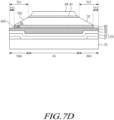
- FIGs. 7A to 7E are cross-sectional views showing a method of manufacturing the display panel of a display device according to embodiments of the present disclosure, and show a method of manufacturing the display panel of the display device of FIGs. 3 and 4 .
- a circuit element layer 20 is formed on a substrate 10, and a first passivation layer 30 is formed on the circuit element layer 20.
- a color filter (not shown) is formed on the first passivation layer 30, and a first overcoat layer 50 is formed to cover the color filter and the first passivation layer 30.
- a second passivation layer 60 is formed on the first overcoat layer 50, and a second overcoat layer 70 is formed on the second passivation layer 60.
- a second trench T21 is formed by etching the second overcoat layer 70 using the mask pattern PR as an etch mask.
- a dry etching process may be used as an etching process.
- a second sloped surface 70S of the second overcoat layer 70 may be exposed through the second trench T21.
- the second sloped surface 70S has a second slope angle ⁇ 2.
- the number of mask patterns is reduced compared to a case where a separate mask pattern is used to form the second trench T21.
- the second trench T21 is formed by etching the second overcoat layer 70 using the mask pattern PR used in forming the first electrode 81, the second trench T21 may be self-aligned with the first electrode 81.
- an etching process for removing the protruding portion of the first electrode 81 may also be carried out.
- a first trench T11 is formed by etching the second passivation layer 60 exposed through the second trench T21. Because the first trench T11 is formed by etching the exposed portion of the second passivation layer 60 by the second trench T21, the first trench T11 may be self-aligned with the second trench T21. A wet etching process may be used as an etching process.
- a first sloped surface 60S of the second passivation layer 60 may be exposed through the first trench T11.
- the first sloped surface 60S has a first slope angle ⁇ 1.
- the etching process is controlled so that the first slope angle ⁇ 1 has a slope angle different from the second slope angle ⁇ 2.
- the etching process may be controlled so that the first slope angle ⁇ 1 has a larger value than the second slope angle ⁇ 2.
- an organic layer 82 is formed on an entire surface including the first electrode 81, the first sloped surface 60S of the second passivation layer 60 and the second sloped surface 70S of the second overcoat layer 70, and a second electrode 83 of a light emitting element is formed on the organic layer 82.
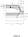
- a circuit element layer 20 may be disposed on a substrate 10, and a first passivation layer 31 may be disposed on the circuit element layer 20.
- the first passivation layer 31 may cover the circuit element layer 20.
- a color filter 40 is disposed on the first passivation layer 31, and a first overcoat layer 51 is disposed on the color filter 40 and the first passivation layer 31.
- the first overcoat layer 51 may be formed without a mask to cover the color filter 40 and the first passivation layer 31.
- a second passivation layer 61 is disposed on the second overcoat layer 71.
- a second trench T22 that exposes the first trench T12 may be formed in the second passivation layer 61.
- a side surface (a second sloped surface) 61S of the second passivation layer 61 may be exposed through the second trench T22.
- the second sloped surface 61S of the second passivation layer 61 exposed through the second trench T22 may have a second slope angle ⁇ 2' different from the first slope angle ⁇ 1'.
- the second slope angle ⁇ 2' may be larger than the first slope angle ⁇ 1'.
- the second sloped surface 61S may have a steeper slope than the first sloped surface 71S.
- the first trench T12 and the second trench T22 may be formed through an etching process using a single mask.
- the top of the first trench T12 may have a dimension larger than the bottom of the second trench T22.
- an undercut structure UDC in which the edge of the first trench T12 is covered with the second passivation layer 61 may be formed.
- An organic layer 82 may be disposed on the first electrode 81, the first sloped surface 71S of the second overcoat layer 71 and the second sloped surface 61S of the second passivation layer 61.
- the organic layer 82 may be formed in common for a plurality of subpixels without a shadow mask.
- the organic layer 82 may have a structure in which a plurality of layers are stacked.
- the organic layer 82 may include a first light emitting unit 82a that is disposed on the first electrode 81, a charge generation layer 82b that is disposed on the first light emitting unit 82a, and a second light emitting unit 82c that is disposed on the charge generation layer 82b.
- the first portion 83a of the second electrode 83 may constitute the light emitting element 80.
- the light emitting element 80 may be constituted by the first electrode 81, the first portion 83a of the second electrode 83 and the organic layer 82 disposed therebetween.
- light may be generated in the organic layer 82 between the first electrode 81 and the first portion 83a of the second electrode 83.
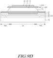
- FIGs. 9A to 9E are cross-sectional views showing a method of manufacturing the display panel of a display device according to embodiments of the present disclosure, and show a method of manufacturing the display panel of the display device of FIG. 8 .
- a second passivation layer 61 is formed on the second overcoat layer 71, and a mask pattern PR is formed on the second passivation layer 61.
- a first trench T12 is formed in the second overcoat layer 71, and a second trench T22 is formed in the second passivation layer 61.
- a dry etching process may be used as an etching method.
- the first trench T12 may have a tapered shape whose dimension decreases toward the top surface of the substrate 10.
- a first sloped surface 71S of the second overcoat layer 71 may be exposed through the first trench T12.
- a second sloped surface 61S of the second passivation layer 61 may be exposed through the second trench T22.
- a first slope angle ⁇ 1' and a second slope angle ⁇ 2' may have different sizes.
- the second slope angle ⁇ 2' may be larger than the first slope angle ⁇ 1'.
- the second sloped surface 61S may have a steeper slope than the first sloped surface 71S.
- a first electrode 81 is formed on the second passivation layer 61.
- the first electrode 81 is formed by forming a conductive layer on the second passivation layer 61, forming a mask pattern (not shown) on the conductive layer and etching the conductive layer using the mask pattern as an etch mask.
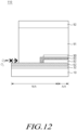
- the display panel of the display device may include a substrate 10.
- a circuit element layer 20 may be disposed on the substrate 10.
- the circuit element layer 20 may include circuit elements (e.g., a driving transistor, a sensing transistor and a storage capacitor), which constitute a subpixel, and wirings 21.
- the first conductive layer may include a light blocking layer (not shown) and a bottom electrode 21a of the storage capacitor.
- the light blocking layer may be disposed to overlap the semiconductor pattern of the driving transistor to protect an oxide semiconductor element from external light.
- the bottom electrode 21a of the storage capacitor may be electrically connected to the gate node of the driving transistor.
- a first passivation layer 32 may be disposed on the circuit element layer 20.
- the first passivation layer 32 may cover the second conductive layer and the buffer layer 22 that is not covered by the second conductive layer.
- the first passivation layer 32 may cover the substrate 10 of the non-active area N/A that is not covered by the buffer layer 22.
- the first passivation layer 32 may contact the top surface of the substrate 10 in the non-active area N/A.
- a color filter 40 may be disposed on the first passivation layer 32.
- the first trench T13 may have a tapered shape whose dimension decreases toward the substrate 10, and the first sloped surface 52S of the overcoat layer 52 exposed by the first trench T13 may have a slope angle ⁇ 1" smaller than 90°.
- a contact hole CH may be formed through the overcoat layer 52 and the first and second passivation layers 32 and 62 to expose the top electrode 23 of the storage capacitor.
- a first electrode 81 is disposed on the overcoat layer 52 to expose the first trench T13.
- the first electrode 81 may extend to the side surface and the bottom surface of the contact hole CH to cover the side surface and the bottom surface of the contact hole CH.
- the first electrode 81 may be connected to the top electrode 23 of the storage capacitor that is disposed on the bottom surface of the contact hole CH.
- the first trench T13 may be formed by etching the overcoat layer 52 that is not covered by the first electrode 81.
- the first trench T13 may be self-aligned with the first electrode 81. Because the first electrode 81 is self-aligned with the first trench T13, the area of the light emitting area EA may be increased to improve aperture ratio.
- the opening width of the first trench T13 may have the same size as a minimum margin between adjacent subpixels. Because the first trench T13 is formed to be self-aligned with the first electrode 81, the opening width of the first trench T13 may be set to the same size as the minimum margin between neighboring subpixels.
- a second electrode 83 of a light emitting element 80 may be disposed on the organic layer 82.
- the second electrode 83 includes a first portion 83a that overlaps the first electrode 81 and a second portion 83b that overlaps the first sloped surface 52S of the overcoat layer 52.
- the second portion 83b of the second electrode 83 has a slope corresponding to the first slope angle ⁇ 1" of the sloped surface 52S of the overcoat layer 52.
- the second portion 83b of the second electrode 83 may play the role of reflecting light emitted from the organic layer 82 and extracting the light to the outside of the display panel.
- the second portion 83b of the second electrode 83 may play the role of increasing light extraction efficiency by reflecting light emitted from the organic layer 82 between the first electrode 81 and the first portion 83a of the second electrode 83.
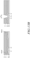
- a first electrode 81 of a light emitting element is formed on the overcoat layer 52.
- the first electrode 81 is formed by forming a conductive layer on the overcoat layer 52, forming a mask pattern PR on the conductive layer and etching the conductive layer using the mask pattern PR as an etch mask. A wet etching process may be used as an etching process.
- the first electrode 81 may be disposed on a light emitting area, may extend from the light emitting area to the contact hole CH formed in a non-light emitting area, and may be connected to the top electrode 23 of the storage capacitor that is exposed through the contact hole CH.
- the edge of the first electrode 81 may protrude beyond the first sloped surface 52S of the overcoat layer 52.
- an additional etching process may be performed to remove the edge of the first electrode 81 that protrudes beyond the first sloped surface 52S of the overcoat layer 52.
- the second sloped surface may have a larger slope angle than the first sloped surface.
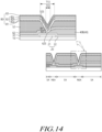
- a display device including a plurality of light emitting areas corresponding to a plurality of subpixels, comprises a substrate; a circuit element layer on the substrate; a first passivation layer on the circuit element layer; a color filter layer on the first passivation layer; a second passivation layer covering the color filter layer; an overcoat layer on the second passivation layer, the overcoat layer having a first trench with a first sloped surface of the overcoat layer at a portion between two neighboring light emitting areas among the plurality of light emitting areas; a first electrode on the overcoat layer and exposing the first trench; an organic layer on the first electrode and the first sloped surface; and a second electrode on the organic layer.
- the first trench may be self-aligned with the first electrode.
- a second sloped surface of the second passivation layer exposed through the second trench may have a different slope angle from the first sloped surface.
- the organic layer may include a charge generation layer that is separated at an area including a boundary between the first sloped surface and the second sloped surface.
- the display device further comprises: a display panel including an active area comprising the plurality of light emitting areas corresponding to the plurality of subpixels, and a non-active area surrounding the active area, wherein the display panel comprises: the substrate; the circuit element layer; the first passivation layer; the color filter layer; the second passivation layer; the overcoat layer; the first electrode; the organic layer; and the second electrode.
- the first passivation layer contacts a top surface of the substrate in an outer part of the display panel, and the second passivation layer contacts a top surface of the first passivation layer.
- a display device includes a display panel including an active area having a plurality of light emitting areas corresponding to a plurality of subpixels and a non-active area surrounding the active area; the display panel including: a substrate; a circuit element layer on the substrate; a first passivation layer on the circuit element layer; a color filter layer on the first passivation layer; a second passivation layer covering the color filter layer; an overcoat layer on the second passivation layer, the overcoat layer having a first trench with a first sloped surface of the overcoat layer at a portion between two neighboring light emitting areas among the plurality of light emitting areas; a first electrode on the overcoat layer and exposing the first trench; an organic layer on the first electrode and the first sloped surface; and a second electrode on the organic layer.
- the display device may further include a third passivation layer covering the second electrode, and an encapsulation layer on the active area and the non-active area, and covering the third passivation layer, and the encapsulation layer may contact the second passivation layer in an outer part of the display panel.
- the first passivation layer and the second passivation layer may extend beyond an end of the encapsulation layer to an edge of the display panel.
- the first passivation layer may contact a top surface of the substrate in an outer part of the display panel, and the second passivation layer may contact a top surface of the first passivation layer.
- the display device may further include a driving circuit in the non-active area of the display panel, and the encapsulation layer may cover the driving circuit.
- the overcoat layer may be absent in the outer part of the display panel.
- a display device that can suppress side leakage current to minimize light emission of an unintended subpixel to improve color gamut and that can minimize the visual recognition of spots or color abnormalities when displaying an image of a low grayscale, to improve display quality.
- a display device that can improve light extraction efficiency to increase the amount of light emitted from the display device so as to increase luminance, can emit a sufficient amount of light at a low voltage to reduce power consumption, and can improve light efficiency to increase a viewing angle and luminance so as to provide a wide viewing angle.
Landscapes
- Engineering & Computer Science (AREA)
- Physics & Mathematics (AREA)
- Microelectronics & Electronic Packaging (AREA)
- Optics & Photonics (AREA)
- Chemical & Material Sciences (AREA)
- Inorganic Chemistry (AREA)
- Electroluminescent Light Sources (AREA)
- Devices For Indicating Variable Information By Combining Individual Elements (AREA)
- Computer Hardware Design (AREA)
- General Physics & Mathematics (AREA)
- Theoretical Computer Science (AREA)
- Geometry (AREA)
Applications Claiming Priority (1)
| Application Number | Priority Date | Filing Date | Title |
|---|---|---|---|
| KR1020230192986A KR20250101399A (ko) | 2023-12-27 | 2023-12-27 | 표시 장치 |
Publications (2)
| Publication Number | Publication Date |
|---|---|
| EP4580368A2 true EP4580368A2 (de) | 2025-07-02 |
| EP4580368A3 EP4580368A3 (de) | 2025-07-30 |
Family
ID=93117488
Family Applications (1)
| Application Number | Title | Priority Date | Filing Date |
|---|---|---|---|
| EP24206136.4A Pending EP4580368A3 (de) | 2023-12-27 | 2024-10-11 | Anzeigevorrichtung |
Country Status (4)
| Country | Link |
|---|---|
| US (1) | US20250221271A1 (de) |
| EP (1) | EP4580368A3 (de) |
| KR (1) | KR20250101399A (de) |
| CN (1) | CN120224972A (de) |
Family Cites Families (7)
| Publication number | Priority date | Publication date | Assignee | Title |
|---|---|---|---|---|
| KR102458864B1 (ko) * | 2015-10-16 | 2022-10-26 | 엘지디스플레이 주식회사 | 유기발광 표시장치 |
| KR102687966B1 (ko) * | 2019-12-30 | 2024-07-23 | 엘지디스플레이 주식회사 | 표시장치 |
| KR102860230B1 (ko) * | 2020-12-22 | 2025-09-15 | 엘지디스플레이 주식회사 | 전계 발광 표시 장치 |
| US12185596B2 (en) * | 2020-12-30 | 2024-12-31 | Lg Display Co., Ltd. | Display device |
| KR20230023841A (ko) * | 2021-08-10 | 2023-02-20 | 삼성디스플레이 주식회사 | 표시 장치 및 그 제조 방법 |
| JPWO2023089447A1 (de) * | 2021-11-19 | 2023-05-25 | ||
| CN116367609A (zh) * | 2021-12-27 | 2023-06-30 | 乐金显示有限公司 | 显示装置及其制造方法 |
-
2023
- 2023-12-27 KR KR1020230192986A patent/KR20250101399A/ko active Pending
-
2024
- 2024-07-29 US US18/786,942 patent/US20250221271A1/en active Pending
- 2024-07-30 CN CN202411028314.2A patent/CN120224972A/zh active Pending
- 2024-10-11 EP EP24206136.4A patent/EP4580368A3/de active Pending
Also Published As
| Publication number | Publication date |
|---|---|
| KR20250101399A (ko) | 2025-07-04 |
| EP4580368A3 (de) | 2025-07-30 |
| CN120224972A (zh) | 2025-06-27 |
| US20250221271A1 (en) | 2025-07-03 |
Similar Documents
| Publication | Publication Date | Title |
|---|---|---|
| US11121198B2 (en) | Organic light emitting display device having auxiliary connection electrode and method of manufacturing the same | |
| TWI760011B (zh) | 顯示裝置及其製造方法 | |
| EP4020572B1 (de) | Anzeigevorrichtung und herstellungsverfahren dafür | |
| US11765948B2 (en) | Display device including a repair pattern to repair a defective pixel and method of repairing same | |
| US20230059253A1 (en) | Display device | |
| US20240138232A1 (en) | Light Emitting Display Device | |
| US20250098416A1 (en) | Display substrate and display apparatus | |
| US20220077269A1 (en) | Display device | |
| US20260020446A1 (en) | Display device with hydrogen blocking layer to minimize diffusion of hydrogen to transistor | |
| US12581823B2 (en) | Display substrate and method for operating the same, and display apparatus | |
| US12464914B2 (en) | Display substrate and method for operating the same, and display apparatus | |
| EP4580368A2 (de) | Anzeigevorrichtung | |
| US20250098449A1 (en) | Display substrate and display apparatus | |
| US11626473B2 (en) | Organic light-emitting diode display device having a second electrode with improved electrical contact with a connection electrode in a contact area | |
| US20250318363A1 (en) | Display device and method of manufacturing the same | |
| US20250056946A1 (en) | Display device | |
| KR20240105009A (ko) | 발광 표시 장치 | |
| TW202527802A (zh) | 顯示設備 |
Legal Events
| Date | Code | Title | Description |
|---|---|---|---|
| PUAI | Public reference made under article 153(3) epc to a published international application that has entered the european phase |
Free format text: ORIGINAL CODE: 0009012 |
|
| STAA | Information on the status of an ep patent application or granted ep patent |
Free format text: STATUS: REQUEST FOR EXAMINATION WAS MADE |
|
| PUAL | Search report despatched |
Free format text: ORIGINAL CODE: 0009013 |
|
| 17P | Request for examination filed |
Effective date: 20241011 |
|
| AK | Designated contracting states |
Kind code of ref document: A2 Designated state(s): AL AT BE BG CH CY CZ DE DK EE ES FI FR GB GR HR HU IE IS IT LI LT LU LV MC ME MK MT NL NO PL PT RO RS SE SI SK SM TR |
|
| AK | Designated contracting states |
Kind code of ref document: A3 Designated state(s): AL AT BE BG CH CY CZ DE DK EE ES FI FR GB GR HR HU IE IS IT LI LT LU LV MC ME MK MT NL NO PL PT RO RS SE SI SK SM TR |
|
| RIC1 | Information provided on ipc code assigned before grant |
Ipc: H10K 59/124 20230101AFI20250620BHEP Ipc: H10K 59/38 20230101ALI20250620BHEP Ipc: H10K 59/80 20230101ALI20250620BHEP Ipc: H10K 50/19 20230101ALN20250620BHEP |