EP4580360A1 - Anzeigesubstrat und anzeigevorrichtung - Google Patents
Anzeigesubstrat und anzeigevorrichtung Download PDFInfo
- Publication number
- EP4580360A1 EP4580360A1 EP22965526.1A EP22965526A EP4580360A1 EP 4580360 A1 EP4580360 A1 EP 4580360A1 EP 22965526 A EP22965526 A EP 22965526A EP 4580360 A1 EP4580360 A1 EP 4580360A1
- Authority
- EP
- European Patent Office
- Prior art keywords
- pixel
- sub
- display substrate
- electrode
- electrode plate
- Prior art date
- Legal status (The legal status is an assumption and is not a legal conclusion. Google has not performed a legal analysis and makes no representation as to the accuracy of the status listed.)
- Pending
Links
Images


Classifications
-
- H—ELECTRICITY
- H10—SEMICONDUCTOR DEVICES; ELECTRIC SOLID-STATE DEVICES NOT OTHERWISE PROVIDED FOR
- H10K—ORGANIC ELECTRIC SOLID-STATE DEVICES
- H10K59/00—Integrated devices, or assemblies of multiple devices, comprising at least one organic light-emitting element covered by group H10K50/00
- H10K59/10—OLED displays
- H10K59/12—Active-matrix OLED [AMOLED] displays
- H10K59/121—Active-matrix OLED [AMOLED] displays characterised by the geometry or disposition of pixel elements
-
- G—PHYSICS
- G09—EDUCATION; CRYPTOGRAPHY; DISPLAY; ADVERTISING; SEALS
- G09G—ARRANGEMENTS OR CIRCUITS FOR CONTROL OF INDICATING DEVICES USING STATIC MEANS TO PRESENT VARIABLE INFORMATION
- G09G3/00—Control arrangements or circuits, of interest only in connection with visual indicators other than cathode-ray tubes
- G09G3/20—Control arrangements or circuits, of interest only in connection with visual indicators other than cathode-ray tubes for presentation of an assembly of a number of characters, e.g. a page, by composing the assembly by combination of individual elements arranged in a matrix no fixed position being assigned to or needed to be assigned to the individual characters or partial characters
- G09G3/22—Control arrangements or circuits, of interest only in connection with visual indicators other than cathode-ray tubes for presentation of an assembly of a number of characters, e.g. a page, by composing the assembly by combination of individual elements arranged in a matrix no fixed position being assigned to or needed to be assigned to the individual characters or partial characters using controlled light sources
- G09G3/30—Control arrangements or circuits, of interest only in connection with visual indicators other than cathode-ray tubes for presentation of an assembly of a number of characters, e.g. a page, by composing the assembly by combination of individual elements arranged in a matrix no fixed position being assigned to or needed to be assigned to the individual characters or partial characters using controlled light sources using electroluminescent panels
- G09G3/32—Control arrangements or circuits, of interest only in connection with visual indicators other than cathode-ray tubes for presentation of an assembly of a number of characters, e.g. a page, by composing the assembly by combination of individual elements arranged in a matrix no fixed position being assigned to or needed to be assigned to the individual characters or partial characters using controlled light sources using electroluminescent panels semiconductive, e.g. using light-emitting diodes [LED]
- G09G3/3208—Control arrangements or circuits, of interest only in connection with visual indicators other than cathode-ray tubes for presentation of an assembly of a number of characters, e.g. a page, by composing the assembly by combination of individual elements arranged in a matrix no fixed position being assigned to or needed to be assigned to the individual characters or partial characters using controlled light sources using electroluminescent panels semiconductive, e.g. using light-emitting diodes [LED] organic, e.g. using organic light-emitting diodes [OLED]
- G09G3/3225—Control arrangements or circuits, of interest only in connection with visual indicators other than cathode-ray tubes for presentation of an assembly of a number of characters, e.g. a page, by composing the assembly by combination of individual elements arranged in a matrix no fixed position being assigned to or needed to be assigned to the individual characters or partial characters using controlled light sources using electroluminescent panels semiconductive, e.g. using light-emitting diodes [LED] organic, e.g. using organic light-emitting diodes [OLED] using an active matrix
- G09G3/3233—Control arrangements or circuits, of interest only in connection with visual indicators other than cathode-ray tubes for presentation of an assembly of a number of characters, e.g. a page, by composing the assembly by combination of individual elements arranged in a matrix no fixed position being assigned to or needed to be assigned to the individual characters or partial characters using controlled light sources using electroluminescent panels semiconductive, e.g. using light-emitting diodes [LED] organic, e.g. using organic light-emitting diodes [OLED] using an active matrix with pixel circuitry controlling the current through the light-emitting element
-
- H—ELECTRICITY
- H10—SEMICONDUCTOR DEVICES; ELECTRIC SOLID-STATE DEVICES NOT OTHERWISE PROVIDED FOR
- H10K—ORGANIC ELECTRIC SOLID-STATE DEVICES
- H10K59/00—Integrated devices, or assemblies of multiple devices, comprising at least one organic light-emitting element covered by group H10K50/00
- H10K59/10—OLED displays
- H10K59/12—Active-matrix OLED [AMOLED] displays
- H10K59/121—Active-matrix OLED [AMOLED] displays characterised by the geometry or disposition of pixel elements
- H10K59/1213—Active-matrix OLED [AMOLED] displays characterised by the geometry or disposition of pixel elements the pixel elements being TFTs
-
- H—ELECTRICITY
- H10—SEMICONDUCTOR DEVICES; ELECTRIC SOLID-STATE DEVICES NOT OTHERWISE PROVIDED FOR
- H10K—ORGANIC ELECTRIC SOLID-STATE DEVICES
- H10K59/00—Integrated devices, or assemblies of multiple devices, comprising at least one organic light-emitting element covered by group H10K50/00
- H10K59/10—OLED displays
- H10K59/12—Active-matrix OLED [AMOLED] displays
- H10K59/121—Active-matrix OLED [AMOLED] displays characterised by the geometry or disposition of pixel elements
- H10K59/1216—Active-matrix OLED [AMOLED] displays characterised by the geometry or disposition of pixel elements the pixel elements being capacitors
-
- H—ELECTRICITY
- H10—SEMICONDUCTOR DEVICES; ELECTRIC SOLID-STATE DEVICES NOT OTHERWISE PROVIDED FOR
- H10K—ORGANIC ELECTRIC SOLID-STATE DEVICES
- H10K59/00—Integrated devices, or assemblies of multiple devices, comprising at least one organic light-emitting element covered by group H10K50/00
- H10K59/10—OLED displays
- H10K59/12—Active-matrix OLED [AMOLED] displays
- H10K59/122—Pixel-defining structures or layers, e.g. banks
-
- H—ELECTRICITY
- H10—SEMICONDUCTOR DEVICES; ELECTRIC SOLID-STATE DEVICES NOT OTHERWISE PROVIDED FOR
- H10K—ORGANIC ELECTRIC SOLID-STATE DEVICES
- H10K59/00—Integrated devices, or assemblies of multiple devices, comprising at least one organic light-emitting element covered by group H10K50/00
- H10K59/10—OLED displays
- H10K59/12—Active-matrix OLED [AMOLED] displays
- H10K59/123—Connection of the pixel electrodes to the thin film transistors [TFT]
-
- H—ELECTRICITY
- H10—SEMICONDUCTOR DEVICES; ELECTRIC SOLID-STATE DEVICES NOT OTHERWISE PROVIDED FOR
- H10K—ORGANIC ELECTRIC SOLID-STATE DEVICES
- H10K59/00—Integrated devices, or assemblies of multiple devices, comprising at least one organic light-emitting element covered by group H10K50/00
- H10K59/10—OLED displays
- H10K59/12—Active-matrix OLED [AMOLED] displays
- H10K59/131—Interconnections, e.g. wiring lines or terminals
- H10K59/1315—Interconnections, e.g. wiring lines or terminals comprising structures specially adapted for lowering the resistance
-
- H—ELECTRICITY
- H10—SEMICONDUCTOR DEVICES; ELECTRIC SOLID-STATE DEVICES NOT OTHERWISE PROVIDED FOR
- H10K—ORGANIC ELECTRIC SOLID-STATE DEVICES
- H10K59/00—Integrated devices, or assemblies of multiple devices, comprising at least one organic light-emitting element covered by group H10K50/00
- H10K59/80—Constructional details
- H10K59/805—Electrodes
- H10K59/8051—Anodes
-
- H—ELECTRICITY
- H10—SEMICONDUCTOR DEVICES; ELECTRIC SOLID-STATE DEVICES NOT OTHERWISE PROVIDED FOR
- H10K—ORGANIC ELECTRIC SOLID-STATE DEVICES
- H10K59/00—Integrated devices, or assemblies of multiple devices, comprising at least one organic light-emitting element covered by group H10K50/00
- H10K59/80—Constructional details
- H10K59/805—Electrodes
- H10K59/8052—Cathodes
-
- H—ELECTRICITY
- H10—SEMICONDUCTOR DEVICES; ELECTRIC SOLID-STATE DEVICES NOT OTHERWISE PROVIDED FOR
- H10K—ORGANIC ELECTRIC SOLID-STATE DEVICES
- H10K59/00—Integrated devices, or assemblies of multiple devices, comprising at least one organic light-emitting element covered by group H10K50/00
- H10K59/80—Constructional details
- H10K59/87—Passivation; Containers; Encapsulations
-
- H—ELECTRICITY
- H10—SEMICONDUCTOR DEVICES; ELECTRIC SOLID-STATE DEVICES NOT OTHERWISE PROVIDED FOR
- H10K—ORGANIC ELECTRIC SOLID-STATE DEVICES
- H10K59/00—Integrated devices, or assemblies of multiple devices, comprising at least one organic light-emitting element covered by group H10K50/00
- H10K59/80—Constructional details
- H10K59/88—Dummy elements, i.e. elements having non-functional features
-
- H—ELECTRICITY
- H10—SEMICONDUCTOR DEVICES; ELECTRIC SOLID-STATE DEVICES NOT OTHERWISE PROVIDED FOR
- H10K—ORGANIC ELECTRIC SOLID-STATE DEVICES
- H10K77/00—Constructional details of devices covered by this subclass and not covered by groups H10K10/80, H10K30/80, H10K50/80 or H10K59/80
- H10K77/10—Substrates, e.g. flexible substrates
-
- G—PHYSICS
- G09—EDUCATION; CRYPTOGRAPHY; DISPLAY; ADVERTISING; SEALS
- G09G—ARRANGEMENTS OR CIRCUITS FOR CONTROL OF INDICATING DEVICES USING STATIC MEANS TO PRESENT VARIABLE INFORMATION
- G09G2300/00—Aspects of the constitution of display devices
- G09G2300/04—Structural and physical details of display devices
- G09G2300/0404—Matrix technologies
- G09G2300/0413—Details of dummy pixels or dummy lines in flat panels
-
- G—PHYSICS
- G09—EDUCATION; CRYPTOGRAPHY; DISPLAY; ADVERTISING; SEALS
- G09G—ARRANGEMENTS OR CIRCUITS FOR CONTROL OF INDICATING DEVICES USING STATIC MEANS TO PRESENT VARIABLE INFORMATION
- G09G2300/00—Aspects of the constitution of display devices
- G09G2300/04—Structural and physical details of display devices
- G09G2300/0421—Structural details of the set of electrodes
- G09G2300/0426—Layout of electrodes and connections
-
- G—PHYSICS
- G09—EDUCATION; CRYPTOGRAPHY; DISPLAY; ADVERTISING; SEALS
- G09G—ARRANGEMENTS OR CIRCUITS FOR CONTROL OF INDICATING DEVICES USING STATIC MEANS TO PRESENT VARIABLE INFORMATION
- G09G2300/00—Aspects of the constitution of display devices
- G09G2300/08—Active matrix structure, i.e. with use of active elements, inclusive of non-linear two terminal elements, in the pixels together with light emitting or modulating elements
- G09G2300/0809—Several active elements per pixel in active matrix panels
- G09G2300/0842—Several active elements per pixel in active matrix panels forming a memory circuit, e.g. a dynamic memory with one capacitor
-
- G—PHYSICS
- G09—EDUCATION; CRYPTOGRAPHY; DISPLAY; ADVERTISING; SEALS
- G09G—ARRANGEMENTS OR CIRCUITS FOR CONTROL OF INDICATING DEVICES USING STATIC MEANS TO PRESENT VARIABLE INFORMATION
- G09G2330/00—Aspects of power supply; Aspects of display protection and defect management
- G09G2330/02—Details of power systems and of start or stop of display operation
- G09G2330/021—Power management, e.g. power saving
Definitions
- Embodiments of the present disclosure relate to a display substrate and a display device.
- the channel of the driving transistor is made of a semiconductor material
- the second electrode plate is a conductor obtained by doping on a same semiconductor material as the channel of the driving transistor.
- two data lines are arranged at two sides of the first power connection line, respectively, and orthographic projections of the two data lines on the base substrate overlap with the orthographic projections of the pixel opening of the first sub-pixel and the pixel opening of the second sub-pixel on the base substrate, respectively.
- two data lines are arranged at two sides of the first power connection line, respectively, and orthographic projections of the two data lines on the base substrate do not overlap with the orthographic projection of the pixel opening of the first sub-pixel on the base substrate, and do not overlap with the orthographic projection of the pixel opening of the second sub-pixel on the base substrate.
- the display substrate further includes a first power line, the first power line is configured to provide a first voltage signal to the pixel circuit, the first power line includes a first power connection line extending in a first direction and a first power signal line extending in a second direction, and an orthographic projection of the first power connection line on the base substrate overlaps with the orthographic projection of the pixel opening on the base substrate, a maximum size of the pixel opening in the second direction is WO, the plurality of sub-pixels include a first sub-pixel and a second sub-pixel that are adjacent to each other in the second direction, a size of one of two first power connection lines in the second direction is Xb1, a size of the other of the two first power connection lines in the second direction is Xb2, and a value range of (Xb1+Xb2)/WO is [0.08, 0.48].
- the display substrate further includes a driving circuit
- the driving circuit is located at one side of the display substrate, one sub-pixel away from the driving circuit has a first brightness L1, one sub-pixel close to the driving circuit has a second brightness L2, and a value range of
- the display substrate further includes two driving circuits, the two driving circuits are located at opposite sides of a display region of the display substrate, one sub-pixel at a central axis of the display substrate has a third brightness L3, one sub-pixel close to one of the two driving circuits has a fourth brightness L4, an extending direction of the central axis of the display substrate is the same as an extending direction of one of the two driving circuits, and a value range of
- a first defining portion is arranged between two pixel openings that are adjacent to each other in a first direction
- a second defining portion is arranged between two pixel openings that are adjacent to each other in a second direction, and the first direction intersects with the second direction
- a thickness of the first defining portion is H1
- a thickness of the second defining portion is H2, and H1 ⁇ H2.
- H1 is less than H2.
- the display substrate further includes an insulating layer, a barrier dam, and an encapsulation layer
- the light-emitting element includes a first electrode, a second electrode, and a light-emitting functional layer located therebetween, and the first electrode of the light-emitting element is connected to the pixel circuit through a via hole penetrating the insulating layer
- the encapsulation layer is configured to encapsulate the light-emitting element
- the encapsulation layer includes a stack of an inorganic encapsulation film and an organic encapsulation film
- an encapsulation adhesive is provided at an outer side of the encapsulation layer
- the insulating layer includes a planarization layer
- the planarization layer includes a first planarization portion and a second planarization portion
- a groove is arranged between the first planarization portion and the second planarization portion
- the barrier dam is located at a periphery of a display region of the display substrate, and an orthographic projection of the barrier
- the display substrate further includes a data line, a first gate line, a second gate line, and a first initialization line
- the pixel circuit further includes a data writing transistor and a first reset transistor, a first electrode of the data writing transistor is connected to the data line, the gate electrode of the driving transistor is connected to a second electrode of the data writing transistor, and a gate electrode of the data writing transistor is connected to the first gate line
- a first electrode of the first reset transistor is connected to the first initialization line
- a second electrode of the first reset transistor is connected to the gate electrode of the driving transistor
- a gate electrode of the first reset transistor is connected to the second gate line
- a dummy sub-pixel is arranged in a vicinity of an edge of the display substrate, the dummy sub-pixel is provided with a dummy driving transistor and a first dummy reset transistor, the first dummy reset transistor is connected to a gate electrode of the dummy driving transistor, and the first dummy reset transistor is disconnected from the first initialization line.
- the display substrate further includes a dummy data line, the dummy data line extends in a first direction, the dummy data line and the data line are insulated from each other, the dummy sub-pixel includes at least two dummy sub-pixels that are adjacent to each other in a second direction, dummy data lines of the at least two dummy sub-pixels are connected to each other.
- the dummy data line is connected to a constant voltage terminal, so as to be configured to provide a constant voltage.
- the at least two dummy sub-pixels include a first dummy sub-pixel, a second dummy sub-pixel, and a third dummy sub-pixel, and three dummy data lines of the first dummy sub-pixel, the second dummy sub-pixel, and the third dummy sub-pixel are connected to each other.
- the display substrate further includes a first power line
- the pixel circuit further includes a light-emitting control transistor, a first electrode of the light-emitting control transistor is connected to the first power line, a second electrode of the light-emitting control transistor is connected to a second electrode of the driving transistor
- the dummy sub-pixel further includes a dummy light-emitting control transistor, a first electrode of the dummy light-emitting control transistor is disconnected from the first power line, and a second electrode of the dummy light-emitting control transistor is connected to a second electrode of the dummy driving transistor.
- the display substrate further includes a pixel defining layer, the pixel defining layer includes a defining portion, the pixel opening is defined by the defining portion, the light-emitting element includes a first electrode and a light-emitting functional layer, the pixel defining layer is configured to expose at least a part of the first electrode of the light-emitting element, and the light-emitting functional layer covers a sidewall of the defining portion.
- the light-emitting element further includes a second electrode
- the light-emitting functional layer is located between the first electrode and the second electrode of the light-emitting element, and the second electrode of the light-emitting element is in contact with a top wall of the defining portion.
- the display substrate further includes an insulating layer
- the first electrode of the light-emitting element is connected to the pixel circuit through a via hole penetrating the insulating layer
- the defining portion includes a first defining portion and a second defining portion, a thickness of the first defining portion is less than a thickness of the second defining portion, and an orthographic projection of the via hole on the base substrate overlaps with an orthographic projection of the first defining portion on the base substrate.
- the display substrate further includes a dummy pixel defining layer, the dummy pixel defining layer includes a plurality of dummy defining portions, and an extending direction of each of the plurality of dummy defining portions is the same as an extending direction of the second defining portion, and a spacing between two adjacent dummy defining portions is greater than a spacing between two adjacent second defining portions.
- the spacing between two adjacent dummy defining portions is 2-20 times the spacing between two adjacent second defining portions.
- the display substrate further includes a second reset transistor, a second initialization line, and an initialization bus
- the initialization bus is arranged at an outer side of a display region of the display substrate
- a first electrode of the second reset transistor is connected to the initialization bus through the second initialization line
- a second electrode of the second reset transistor is connected to the light-emitting element through the driving transistor
- the second reset transistor is connected to a row of sub-pixels, and in terms of a same row of sub-pixels, a count of second reset transistors is less than a count of sub-pixels.
- the display substrate further includes a light-emitting control transistor, a first power line, and a first power bus
- the first power line is configured to provide a first voltage signal to the pixel circuit
- the first power line is connected to the first power bus
- a first electrode of the light-emitting control transistor is connected to the first power line
- a second electrode of the light-emitting control transistor is connected to a second electrode of the driving transistor, a count of light-emitting control transistors of sub-pixels in one row is less than a count of sub-pixels in the row.
- a count of light-emitting control transistors of sub-pixels in one row is greater than a count of second reset transistors in the row.
- the second electrode plate is arranged in a same layer as the channel of the driving transistor, the second electrode plate is closer to the base substrate than the first electrode plate, and an orthographic projection of the second electrode plate on the base substrate overlaps with the orthographic projection of the pixel opening on the base substrate.
- Embodiments of the present disclosure further provides a display substrate, including: a base substrate and a plurality of sub-pixels disposed on the base substrate; each of the plurality of sub-pixels includes: a pixel circuit, including a driving transistor and a storage capacitor, the storage capacitor including a first electrode plate and a second electrode plate, the first electrode plate of the storage capacitor being connected to a gate electrode of the driving transistor, and the second electrode plate of the storage capacitor being connected to a first electrode of the driving transistor; and a light-emitting element, electrically connected to the pixel circuit, the pixel circuit being configured to drive the light-emitting element, the sub-pixel includes a pixel opening, the pixel opening is configured to define a light-emitting region of the sub-pixel, an orthographic projection of the storage capacitor on the base substrate overlaps with an orthographic projection of the pixel opening on the base substrate, an orthographic projection of a channel of the driving transistor on the base substrate overlaps with the orthographic projection of the pixel opening on the base substrate,
- Embodiments of the present disclosure further provides a display substrate, including: a base substrate and a plurality of sub-pixels disposed on the base substrate; each of the plurality of sub-pixels includes: a pixel circuit, including a driving transistor and a storage capacitor, the storage capacitor including a first electrode plate and a second electrode plate, the first electrode plate of the storage capacitor being connected to a gate electrode of the driving transistor, and the second electrode plate of the storage capacitor being connected to a first electrode of the driving transistor; and a light-emitting element, electrically connected to the pixel circuit, the pixel circuit being configured to drive the light-emitting element, the sub-pixel includes a pixel opening, the pixel opening is configured to define a light-emitting region of the sub-pixel, an orthographic projection of the storage capacitor on the base substrate overlaps with an orthographic projection of the pixel opening on the base substrate, an orthographic projection of a channel of the driving transistor on the base substrate overlaps with the orthographic projection of the pixel opening on the base substrate,
- Embodiments of the present disclosure further provides a display substrate, including: a base substrate and a plurality of sub-pixels disposed on the base substrate; each of the plurality of sub-pixels includes: a pixel circuit, including a driving transistor and a storage capacitor, the storage capacitor including a first electrode plate and a second electrode plate, the first electrode plate of the storage capacitor being connected to a gate electrode of the driving transistor, and the second electrode plate of the storage capacitor being connected to a first electrode of the driving transistor; and a light-emitting element, electrically connected to the pixel circuit, the pixel circuit being configured to drive the light-emitting element, the sub-pixel includes a pixel opening, the pixel opening is configured to define a light-emitting region of the sub-pixel, an orthographic projection of the storage capacitor on the base substrate overlaps with an orthographic projection of the pixel opening on the base substrate, an orthographic projection of a channel of the driving transistor on the base substrate overlaps with the orthographic projection of the pixel opening on the base substrate,
- Embodiments of the present disclosure further provides a display substrate, including: a base substrate and a plurality of sub-pixels disposed on the base substrate; each of the plurality of sub-pixels includes: a pixel circuit, including a driving transistor and a storage capacitor, the storage capacitor including a first electrode plate and a second electrode plate, the first electrode plate of the storage capacitor being connected to a gate electrode of the driving transistor, and the second electrode plate of the storage capacitor being connected to a first electrode of the driving transistor; and a light-emitting element, electrically connected to the pixel circuit, the pixel circuit being configured to drive the light-emitting element, the sub-pixel includes a pixel opening, the pixel opening is configured to define a light-emitting region of the sub-pixel, an orthographic projection of the storage capacitor on the base substrate overlaps with an orthographic projection of the pixel opening on the base substrate, an orthographic projection of a channel of the driving transistor on the base substrate overlaps with the orthographic projection of the pixel opening on the base substrate,
- Embodiments of the present disclosure further provides a display substrate, including: a base substrate and a plurality of sub-pixels disposed on the base substrate; each of the plurality of sub-pixels includes: a pixel circuit, including a driving transistor and a storage capacitor, the storage capacitor including a first electrode plate and a second electrode plate, the first electrode plate of the storage capacitor being connected to a gate electrode of the driving transistor, and the second electrode plate of the storage capacitor being connected to a first electrode of the driving transistor; and a light-emitting element, electrically connected to the pixel circuit, the pixel circuit being configured to drive the light-emitting element, the sub-pixel includes a pixel opening, the pixel opening is configured to define a light-emitting region of the sub-pixel, an orthographic projection of the storage capacitor on the base substrate overlaps with an orthographic projection of the pixel opening on the base substrate, an orthographic projection of a channel of the driving transistor on the base substrate overlaps with the orthographic projection of the pixel opening on the base substrate,
- Embodiments of the present disclosure further provides a display substrate, including: a base substrate and a plurality of sub-pixels disposed on the base substrate; each of the plurality of sub-pixels includes: a pixel circuit, including a driving transistor and a storage capacitor, the storage capacitor including a first electrode plate and a second electrode plate, the first electrode plate of the storage capacitor being connected to a gate electrode of the driving transistor, and the second electrode plate of the storage capacitor being connected to a first electrode of the driving transistor; and a light-emitting element, electrically connected to the pixel circuit, the pixel circuit being configured to drive the light-emitting element, the sub-pixel includes a pixel opening, the pixel opening is configured to define a light-emitting region of the sub-pixel, an orthographic projection of the storage capacitor on the base substrate overlaps with an orthographic projection of the pixel opening on the base substrate, an orthographic projection of a channel of the driving transistor on the base substrate overlaps with the orthographic projection of the pixel opening on the base substrate,
- the display substrate can also satisfy a following relationship: a value range of (W*L+S2)*M1/M2 is [0.014, 0.133], where M1 is a count of pixel openings in the display substrate, and M2 is an area of the display substrate.
- Embodiments of the present disclosure further provides a display device, including any one of the display substrates as described above.
- the organic light-emitting layer needs to be completed by an evaporation process, and the process conditions are demanding and it is difficult to achieve a large-area design.
- inkjet printing to manufacturing OLED luminescent material layer is the best way to realize low-cost OLED production, and enable OLED displays to compete in the middle-end and high-end market.
- Inkjet printing is an efficient process. Compared with evaporation, inkjet printing has less material waste and is very quick.
- the main method is to dissolve the organic material by using a solvent to form a solution (ink), and then directly spray the solution (ink) onto the surface of the base substrate to form a light-emitting functional layer of a sub pixel, such as a red (R) sub-pixel, a green (G) sub-pixel, a blue (B) sub-pixel, etc.
- a sub pixel such as a red (R) sub-pixel, a green (G) sub-pixel, a blue (B) sub-pixel, etc.
- Inkjet printing OLED technology has significant advantages over evaporation technology in terms of production process, yield, and cost, etc.
- the light-emitting functional layer includes a plurality of film layers, such as a light-emitting layer (a luminescent material layer); and the light-emitting functional layer can further include at least one of a hole injection layer, a hole transport layer, an electron transport layer, and an electron injection layer, etc.
- the organic light-emitting functional layer can be selected as needed.
- At least one film layer in the light-emitting functional layer can be manufactured by inkjet printing process.
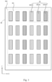
- each sub-pixel 100 includes a pixel circuit 100a and a light-emitting element 100b, the pixel circuit 100a is electrically connected to the light-emitting element 100b, and the pixel circuit 100a is configured to drive the light-emitting element 100b.
- the pixel circuit 100a is configured to drive the light-emitting element 100b to emit light.
- the light-emitting element 100b includes a light-emitting region.
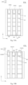
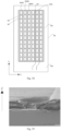
- the pixel arrangement shown in Fig. 1 refers to the arrangement position of the light-emitting regions of the light-emitting elements 100b in the sub-pixels 100.
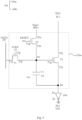
- the pixel circuit 100a includes a data writing transistor T1, a reset transistor T2, a driving transistor T3, and a storage capacitor Cst, and the light-emitting element 100b is connected to the driving transistor T3.
- the reset transistor T2 is configured to reset the gate electrode T3g of the driving transistor T3.
- the storage capacitor Cst includes a first terminal C1 and a second terminal C2.
- the gate line G1 is configured to provide a scan signal SCAN to the sub-pixel 100
- the gate line G2 is configured to provide a reset control signal RESET1 to the sub-pixel 100
- the data line DT is configured to provide a data signal (data voltage) DATA to the sub-pixel 100.
- the initialization line INT1 is configured to provide an initialization signal Vinit1 to the sub-pixel 100.
- the driving transistor T3 is electrically connected to the light-emitting element 100b, and outputs a driving current to drive the light-emitting element 100b to emit light under the control of the signals, such as the scan signal SCAN, the data signal DATA, the first voltage signal VDD, the second voltage signal VSS, etc.
- the first electrode E1 of the light-emitting element 100b is connected to the first electrode T3a of the driving transistor T3, the second electrode E2 of the light-emitting element 100b is connected to the second power line PL2, the second electrode T3b of the driving transistor T3 is connected to the first power line PL1, the gate electrode T3g of the driving transistor T3 is connected to the second electrode T1b of the data writing transistor T1, the first electrode T1a of the data writing transistor T1 is connected to the data line DT, and the gate electrode T1g of the data writing transistor T1 is connected to the gate line G1.
- the first electrode T2a of the reset transistor T2 is connected to the initialization line INT1
- the second electrode T2b of the reset transistor T2 is connected to the gate electrode T3g of the driving transistor T3
- the gate electrode T2g of the reset transistor T2 is connected to the gate line G2.
- the first terminal C1 of the storage capacitor Cst is also connected to the second electrode T2b of the reset transistor T2.
- the gate electrode T3g of the driving transistor T3, the first terminal C1 of the storage capacitor Cst, the second electrode T1b of the data writing transistor T1, and the second electrode T2b of the reset transistor T2 are connected to each other, all of which are connected to a node N1 and have the same potential.
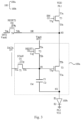
- the display substrate further includes an initialization line INT2, and the initialization line INT2 is configured to provide an initialization signal Vinit2 to the reset transistor T4.
- the second electrode T4b of the reset transistor T4 is connected to the first electrode E1 of the light-emitting element 100b through the driving transistor T3, the first electrode T3a of the driving transistor T3 is connected to the first electrode E1 of the light-emitting element 100b, and the second electrode T3b of the driving transistor T3 is connected to the second electrode T4b of the reset transistor T4.
- the initialization signal Vinit1 and the initialization signal Vinit2 are constant voltage signals, which can be, for example, between the first voltage signal VDD and the second voltage signal VSS, but are not limited thereto.
- the initialization signal Vinit1 and the initialization signal Vinit2 can both be less than or equal to the second voltage signal VSS.
- the initialization line INT1 and the initialization line INT2 are connected and are both configured to provide the same initialization signal, that is, the initialization signal Vinit1 and the initialization signal Vinit2 are equal, but are not limited thereto.
- the initialization line INT1 and the initialization line INT2 are insulated from each other to provide different initialization signals.
- the second electrode T3b of the driving transistor T3 is directly connected to the first power line PL1.
- the display substrate further includes a gate line G5 and a light-emitting control transistor T5, the gate line G5 is configured to provide a light-emitting control signal EM to the light-emitting control transistor T5, and the second electrode T3b of the driving transistor T3 is connected to the first power line PL1 through the light-emitting control transistor T5.
- the first electrode T5a of the light-emitting control transistor T5 is connected to the first power line PL1
- the second electrode T5b of the light-emitting control transistor T5 is connected to the second electrode T3b of the driving transistor T3
- the gate electrode T5g of the light-emitting control transistor T5 is connected to the gate line G5.
- the second electrode T5b of the light-emitting control transistor T5, the second electrode T4b of the reset transistor T4, and the second electrode T3b of the driving transistor T3 are connected to each other, all of which are connected to a node N3 and have the same potential.
- the plurality of sub-pixels 100 include a first sub-pixel 101, a second sub-pixel 102, and a third sub-pixel 103.
- the first sub-pixel 101, the second sub-pixel 102, and the third sub-pixel 103 are sequentially arranged in the second direction X.
- the sub-pixels in one pixel can also be arranged in other ways.
- the driving transistor T3 is a dual-gate transistor, which includes a sub-transistor T31 and a sub-transistor T32. As shown in Fig. 4 , the sub-transistor T31 and the sub-transistor T32 are connected in series. Fig. 4 is illustrated by taking that the driving transistor T3 is a dual-gate transistor as an example. In some other embodiments, besides the driving transistor T3, other transistors can also be set as dual-gate transistors. That is, each transistor in the pixel circuit can be set as a single-gate transistor or a dual-gate transistor as needed.
- the display substrate includes a reset signal transmission line INI, and the second electrode T4b of the reset transistor T4 is connected to the second electrode T3b (node N3) of the driving transistor through the reset signal transmission line INI.
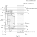
- Fig. 5 is a layout diagram of a display substrate provided by an embodiment of the present disclosure.
- Fig. 6 is a cross-sectional view taken along line A1-A2 of Fig. 5 .
- Fig. 7A-Fig. 7G1 are plan views of a single layer of the display substrate in Fig. 5 .
- Fig. 8A-Fig. 8E are plan views of part of stacked layers of the display substrate in Fig. 5 .
- Fig. 8F is a schematic diagram of a width and length of a channel of a driving transistor in the display substrate of Fig. 5 .
- the display substrate includes a base substrate BS, and a barrier layer BR and a buffer layer BF which are located on the base substrate BS.
- the buffer layer BF is provided thereon with an active layer LY0 and a gate insulating layer GI located on the active layer LY0, a first conductive pattern layer LY1 is located on the gate insulating layer GI, an interlayer insulating layer ILD is located on the first conductive pattern layer LY1, a second conductive pattern layer LY2 is located on the interlayer insulating layer ILD, an insulating layer ISL is located on the second conductive pattern layer LY2, and a first electrode layer LY3 is located on the insulating layer ISL.
- Fig. 5 and Fig. 6 show a first terminal C1 and a second terminal C2 of the storage capacitor Cst.
- the first terminal C1 includes a first electrode plate Ca (as shown in Fig. 7B )
- the second terminal C2 includes a second electrode plate Cb (as shown in Fig. 7A ) and a third electrode plate Cc (as shown in Fig. 7D ).
- the first conductive pattern layer LY1 is closer to the base substrate BS than the second conductive pattern layer LY2.
- the display substrate provided by an embodiment of the present disclosure includes: a base substrate BS and sub-pixels 100 disposed on the base substrate BS.
- a plurality of sub-pixels 100 can be provided.
- the display substrate further includes a pixel defining layer PDL
- the sub-pixel 100 includes a pixel opening P0
- the pixel opening P0 is configured to expose at least a part of the first electrode E1
- the pixel opening P0 is configured to define a light-emitting region of the sub-pixel 100.
- the slope angle of the portion of the pixel defining layer PDL that defines the pixel opening P0 is in the range of 40-65 degrees.
- the sub-pixel 100 includes a pixel circuit 100a and a light-emitting element 100b
- the pixel circuit 100a includes the storage capacitor Cst
- the second electrode plate Cb is closer to the base substrate BS than the first electrode plate Ca
- the first electrode plate Ca is closer to the base substrate BS than the third electrode plate Cc
- the light-emitting element 100b includes a first electrode E1, a second electrode E2, and a light-emitting functional layer FL located between the first electrode E1 and the second electrode E2
- the pixel circuit 100a is configured to drive the light-emitting element 100b.
- each film layer of the light-emitting functional layer FL is formed by inkjet printing, that is, each film layer of the light-emitting functional layer FL is provided in the pixel opening P0.
- some film layers in the light-emitting functional layer FL can be formed by inkjet printing, and some other film layers in the light-emitting functional layer FL can be formed by evaporation, and the film layers formed by evaporation can be common layers; and an embodiment of this situation can refer to Fig. 45 .
- a plan view shows a first direction Y and a second direction X
- a cross-sectional view shows a third direction Z.
- Both the first direction Y and the second direction X are parallel to a main surface of the base substrate BS.
- the third direction Z is a direction perpendicular to the main surface of the base substrate BS.
- the first direction Y and the second direction X are intersected.
- the embodiment of the present disclosure is illustrated by taking that the first direction Y is perpendicular to the second direction X as an example.
- the main surface of the base substrate BS is a surface of the base substrate BS for manufacturing various elements.
- the upper surface of the base substrate BS is the main surface of the base substrate BS.
- the first power line PL1 includes a first power signal line PL11 extending in the second direction X and a first power connection line PL12 extending in the first direction Y, and the first power signal line PL11 is connected to the first power connection line PL12.
- the data line DT extends in the first direction Y and the data line DT is formed in segments.
- the data line DT includes a first part DTa, a second part DTb, and a third part DTc; the first part DTa and the third part DTc are connected through the second part DTb; the first part DTa and the third part DTc are located in the first conductive pattern layer LY1, and the second part DTb is located in the second conductive pattern layer LY2.
- elements located in the second conductive pattern layer LY2 can be connected to elements located in the first conductive pattern layer LY1 and elements located in the active layer LY0 through via holes, and elements located in the first conductive pattern layer LY1 and elements located in the active layer LY0 can be connected through elements located in the second conductive pattern layer LY2.
- insulating layers penetrated by a via hole can depend on the insulating layers between two conductive pattern layers connected through the via hole.
- the active layer LY0, the first conductive pattern layer LY1, and the second conductive pattern layer LY2 are used to form a pixel circuit 100a, so as to simplify the manufacturing process and reduce the thickness of the display substrate.
- the initialization line INT1 and/or the first power line PL1 can be referred to as conductive structures 40; the conductive structure 40 includes a signal transmission line 411 and a signal connection line 412, the conductive structure 40 is configured to provide a voltage signal to the sub-pixel 100, the signal transmission line 411 extends in the second direction X, the signal connection line 412 extends in the first direction Y, and the signal connection line 412 is electrically connected to the signal transmission line 411.
- the conductive structure 40 adopts a mesh structure, and includes a part extending in the first direction Y (i.e., signal connection line 412) and a part extending in the second direction X (i.e., signal transmission line 411), respectively.
- the first power line PL1 of the pixel circuit 100a is formed by using two conductive pattern layers. As shown in Fig. 5 , Fig. 7B and Fig. 7D , parts of the first power line PL1 extending in the first direction Y are all formed in segments. As shown in Fig. 5 and Fig. 7D , parts of the first power line PL1 extending in the second direction X are all located in the second conductive pattern layer LY2.
- the signal connection line 412 includes a first part 412a, a second part 412b, and a third part 412c; the first part 412a and the third part 412c are connected through the second part 412b, the first part 412a and the third part 412c are located in the first conductive pattern layer LY1, and the second part 412b is located in the second conductive pattern layer LY2.
- the signal connection line 412 includes a first power connection line PL12.
- a first part PLa and a second part PLb of the first power connection line PL12 are connected through a via hole Va, and the second part PLb and a third part PLc of the first power connection line PL12 are connected through a via hole Vb.
- Fig. 7C shows an interlayer insulating layer ILD, which is represented by via holes in the interlayer insulating layer ILD.
- Fig. 7C shows via holes V1-V13, via holes Va-Vd, and a via hole V0.
- Fig. 7E shows an insulating layer ISL, which is represented by via holes in the insulating layer ISL.
- Fig. 7E shows a via hole VH.
- Fig. 7F shows a first electrode layer LY3 of the light-emitting element.
- Fig. 7F shows a first electrode E1.
- Fig. 7G shows a pixel defining layer PDL, which is represented by a pixel opening P0 in the pixel defining layer PDL.
- the pixel opening P0 corresponds to an effective light-emitting region of the sub-pixel.
- the film layer manufactured by inkjet printing is located in the pixel opening P0 of the pixel defining layer PDL.
- the first power signal line PL11 and the first power connection line PL12 are connected through the via hole V0.
- connection electrode CEa is connected to the gate line G5 through the via hole V9, and the connection electrode CEa serves as the gate electrode of the light-emitting control transistor T5.
- connection electrode CEb one end of the connection electrode CEb is connected to the first power line PL1 (first power signal line PL11) through the via hole V11, and the other end of the connection electrode CEb is connected to the first electrode T5a of the light-emitting control transistor T5 through the via hole V10.
- the data line DT is connected to the first electrode T1a of the data writing transistor T1 through the via hole V4.
- connection electrode CEd is connected to the gate line G2 through the via hole V6, and the connection electrode CEd serves as the gate electrode of the reset transistor T2.
- connection electrode CEe one end of the connection electrode CEe is connected to the initialization line INT1 (initialization signal line INT11) through the via hole V7, and the other end of the connection electrode CEe is connected to the first electrode T2a of the reset transistor T2 through the via hole V8.
- connection electrode CEf one end of the connection electrode CEf is connected to the first terminal C1 (first electrode plate Ca, gate electrode of the driving transistor T3) through the via hole V3, and the other end of the connection electrode CEf is connected to the second electrode T1b of the data writing transistor T1 (i.e., second electrode T2b of the reset transistor T2) through the via hole V5.
- the third electrode plate Cc of the second terminal C2 is connected to the second electrode plate Cb of the second terminal C2 (i.e., first electrode T3a of the driving transistor T3) through the via hole V2.
- the reset signal transmission line INI is connected to the first electrode T3a of the driving transistor T3 through the via hole V1
- the reset signal transmission line INI is connected to the second electrode T5b of the light-emitting control transistor T5 through the via hole V13.
- the second electrode T5b of the light-emitting control transistor T5 and the second electrode T3b of the driving transistor T3 are connected through the reset signal transmission line INI.
- a first plate-shaped portion Cba and a second plate-shaped portion Cbb can both be connected to the channel T3c of the driving transistor T3, and the first plate-shaped portion Cba, the second plate-shaped portion Cbb, and the channel T3c of the driving transistor T3 are located in the same layer.
- the first plate-shaped portion Cba, the second plate-shaped portion Cbb, and the channel T3c of the driving transistor T3 are of an integral structure.
- the display substrate provided by the embodiment of the present disclosure, by the pattern design of the active layer L0 matching the pattern design of the channel of the driving transistor and the capacitor electrode plate located in the active layer, the balance relationship between luminescent uniformity and power consumption is optimized, the luminescent uniformity of the display substrate is improved, and the power consumption is reduced.
- the first plate-shaped portion Cba includes a first part PR1 and a second part PR2, the first part PR1 extends in the first direction Y, the second part PR2 extends in the second direction X, and the first part PR1 and the second plate-shaped portion Cbb are opposite to each other and are respectively arranged at both sides of the channel T3c of the driving transistor T3 in the second direction X.
- the first part PR1, the second part PR2, and the second plate-shaped portion Cbb are divided by dashed lines.
- the second electrode plate Cb and the channel of the driving transistor T3 are of an integral structure and can be formed by the same thin film through the same patterning process.
- the material of the channel of the driving transistor T3 is a semiconductor material
- the second electrode plate Cb is a conductor obtained by doping on the semiconductor material.
- Fig. 8B shows a channel T1c of the data writing transistor T1, a channel T2c of the reset transistor T2, a channel T3c of the driving transistor T3, and a channel T5c of the light-emitting control transistor T5.
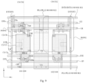
- Fig. 9 is a layout diagram of a display substrate provided by an embodiment of the present disclosure.
- Fig. 10 is a layout diagram of a display substrate provided by another embodiment of the present disclosure.
- Fig. 11 is a layout diagram of a display substrate provided by another embodiment of the present disclosure.
- Fig. 9 shows two sub-pixels 100: a first sub-pixel 101 and a second sub-pixel 102.
- the first sub-pixel 101 and the second sub-pixel 102 are adjacent to each other and arranged in sequence in the second direction X.
- the layout of the pixel circuit of the first sub-pixel 101 and the layout of the pixel circuit of the second sub-pixel 102 are arranged in a mirror symmetry manner.
- the pixel circuit of the first sub-pixel 101 and the pixel circuit of the second sub-pixel 102 are axisymmetric, and are axisymmetric with respect to a straight line extending in the first direction Y.
- the pixel opening P0 (pixel opening P01) of the first sub-pixel 101 and the pixel opening P0 (pixel opening P02) of the second sub-pixel 102 overlap with the first power line PL1 (first power connection line PL12), respectively. That is, the orthographic projection of the pixel opening P01 on the base substrate overlaps with the orthographic projection of the first power line PL1 (first power connection line PL12) on the base substrate, and the orthographic projection of the pixel opening P02 on the base substrate overlaps with the orthographic projection of the first power line PL1 (first power connection line PL12) on the base substrate.
- the part of the first power line PL1 (first power connection line PL12) directly below the opening P0 can play the role of leveling, which further improves the flatness of the light-emitting layer to alleviate the color shift, and for example, to alleviate the color shift at the left and right viewing angles, and further improve the display quality. That is, the central axis of the third electrode plate Cc of the storage capacitor in the first direction Y is closer to the central axis C0 of the pixel opening P0 extending in the first direction Y, and the positions of the pixel opening P0 at both sides of the third electrode plate Cc are leveled with signal lines.
- the two adjacent sub-pixels respectively overlap with the first power connection line PL12, and the embodiment of the present disclosure includes but is not limited to this case.
- one of two adjacent sub-pixels may overlap with the first power connection line PL12, and the other of the two adjacent sub-pixels may not overlap with the first power connection line PL12.
- the third electrode plate Cc and the first power connection line PL12 are respectively arranged at both sides of the central axis C0.
- the proportion of the first power line PL1 (first power connection line PL12) in the width direction (second direction X) of the pixel opening is larger, that is, the leveling size of the first power connection line PL12 in the width direction of the pixel opening is larger, so that the third electrode plate Cc and the first power connection line PL12, which are located at both sides of the central axis C0, play a leveling role together, so as to improve the flatness of the light-emitting layer and alleviate color shift, for example, alleviate color shift at the left and right viewing angels.
- Fig. 10 shows that the third sub-pixel 103 and the first sub-pixel 101 are adjacent to each other and arranged in sequence in the second direction X.
- Fig. 12 is a layout diagram of a display substrate provided by another embodiment of the present disclosure. Compared with the display substrate shown in Fig. 5 , in the display substrate shown in Fig. 12 , the connection electrode CEb is located in the active layer L0, and the connection electrode CEb and the first electrode T5a of the light-emitting control transistor T5 are of an integral structure.
- Xd1 1.57 microns
- Xd2 1.73 microns
- Xd1/Xd2 0.9.
- Xd1 1.73 microns
- Xd2 1.57 microns
- Xd1/Xd2 1.1.
- Xd1 and Xd2 are not limited to the above values, and can be determined as needed.
- the display substrate further includes a plurality of signal lines 80 located at one side of the storage capacitor Cst (the storage capacitor Cst is shown by the third electrode plate Cc in Fig. 25 ), the orthographic projections of the plurality of signal lines 80 on the base substrate BS overlap with the orthographic projection of the pixel opening P0 on the base substrate BS, the signal line 80 extends in the second direction X, the distance between the third electrode plate Cc and a signal line closest to the third electrode plate Cc is Xd3, the width of the signal line is Xd4, and the value range of Xd3/Xd4 is [0.9, 1.1], which is helpful to improve the leveling effect of the signal line 80 and the third electrode plate Cc on the bottom surface of the pixel opening of the sub-pixel, alleviate the color shift between the up and down directions, and improve the consistency of the color shift between the up and down directions.
- the display substrate further satisfies at least one of the following settings: W2/W1 ⁇ 0.9, the value range of 2 ⁇ W2/WO is [0.71, 0.99], the value range of cross voltage Uc(V)/size Lg(inch) is [0.32, 0.74], the value range of Xd1/Xd2 is [0.9, 1.1], the value range of Xd3/Xd4 is [0.9, 1.1], and the value range of DP/WO is [0.01, 0.19], so that the display substrate satisfies that ⁇ U ⁇ 0.0020.That is, by the design of at least one of the above sizes, the color shift of the display substrate is relatively small.
- the display substrate further includes a first signal line 801, the first signal line 801 extends in the first direction Y, the sub-pixels 100 include a first sub-pixel 101 and a second sub-pixel 102 that are adjacent to each other in the second direction X, the first signal line 801 is configured to provide a data signal to the pixel circuit 100a of the first sub-pixel 101, the pixel opening P0 of the first sub-pixel 101 and the pixel opening P0 of the second sub-pixel 102 are separated from each other, and the first signal line 801 is located between the pixel opening P0 of the first sub-pixel 101 and the pixel opening P0 of the second sub-pixel 102.
- the minimum distance between the pixel opening P0 of the first sub-pixel 101 and the first signal line 801 is Xa1
- the minimum distance between the pixel opening P0 of the second sub-pixel 102 and the first signal line 801 is Xa2
- the value range of Xa1/Xa2 is [0.8, 1.2].
- the first signal line 801 extends in the first direction Y and is located between the pixel openings P0 of adjacent sub-pixels.
- the body material of the pixel defining layer is arranged directly on the first signal line 801.
- Xa1 12 microns
- Xa2 12 microns
- Xa1/Xa2 1.
- Xa1 and Xa2 can fluctuate up and down on the basis of the above values, as long as the value range of Xa1/Xa2 is [0.8, 1.2].
- the display substrate further includes a second signal line 802, the second signal line 802 extends in the first direction Y, the first signal line 801 and the second signal line 802 are located at opposite sides of the same third electrode plate Cc, and the orthographic projection of the second signal line 802 on the base substrate BS overlaps with the orthographic projection of the pixel opening P0 of the second sub-pixel 102 on the base substrate BS.
- the spacing between the third electrode plate Cc and the second signal line 802 is Xa3
- the spacing between the third electrode plate Cc and the first signal line 801 is Xa4
- the value range of Xa3/Xa4 is [0.8, 1.2], so as to enhance the leveling effect of the third electrode plate Cc and the second signal line 802 on the bottom surface of the pixel opening of the second sub-pixel 102, improve the flatness of the light-emitting layer, and alleviate the color shift.
- Xa3 8.6 microns
- Xa4 10 microns
- Xa3/Xa4 0.86.
- Xa3 and Xa4 can fluctuate up and down on the basis of the above values, as long as the value range of Xa3/Xa4 is [0.8, 1.2].
- the display substrate further includes a third signal line 803, the third signal line 803 extends in the first direction Y, the orthographic projection of the third signal line 803 on the base substrate BS overlaps with the orthographic projection of the pixel opening P0 of the first sub-pixel 101 on the base substrate BS, the minimum distance between the third electrode plate Cc of the first sub-pixel 101 and the third signal line 803 is Xa5, the minimum distance between the third signal line 803 and the first signal line 801 is Xa6, and the value range of Xa5/Xa6 is [0.8, 1.2], so as to enhance the leveling effect of the third electrode plate Cc and the third signal line 803 on the bottom surface of the pixel opening of the first sub-pixel 101, improve the flatness of the light-emitting layer, and alleviate the color shift.
- the third signal line 803 extends in the first direction Y
- the orthographic projection of the third signal line 803 on the base substrate BS overlaps with the orthographic projection of the pixel opening P0 of the first
- Xa5 8.7 microns
- Xa6 7.3 microns
- Xa5/Xa6 1.2.
- Xa5 and Xa6 can fluctuate up and down on the basis of the above values, as long as the value range of Xa5/Xa6 is [0.8, 1.2].
- the first signal line 801 includes a data line DT
- at least one of the second signal line 802 and the third signal line 803 includes a first power connection line PL12 or an initialization connection line INT12.
- Fig. 26 is illustrated by taking that the second signal line 802 and the third signal line 803 are both first power connection lines PL12 as an example.
- the second signal line 802 is the first power connection line PL12
- the third signal line 803 is the initialization connection line INT12.
- the third signal line 803, the first signal line 801, and the second signal line 802 are sequentially arranged in the second direction X.
- Fig. 27 is a plan view of a display substrate provided by an embodiment of the present disclosure.
- Fig. 28 is a plan view of a display substrate provided by an embodiment of the present disclosure.
- the display substrate further includes a data line DT and a first power line PL1, the data line DT is configured to provide a data voltage to the pixel circuit 100a, the date line extends in the first direction Y, the first power line PL1 is configured to provide a first voltage signal VDD to the pixel circuit 100a, the first power line PL1 includes a first power connection line PL12 extending in the first direction Y and a first power signal line PL11 extending in the second direction X, the sub-pixels 100 include a sub-pixel 121 and a sub-pixel 122 that are adjacent to each other in the second direction X, and the orthographic projection of the first power connection line PL12 on the base substrate overlaps with the pixel opening P0 of the sub-pixel 121
- FIG. 27 shows a data line DT1 and a data line DT2, the data line DT1 and the data line DT2 provide data voltages for the sub-pixel 121 and the sub-pixel 122, respectively; and the orthographic projections of the data line DT1 and the data line DT2 on the base substrate overlap with the orthographic projections of the pixel opening P01 of the sub-pixel 121 and the pixel opening P02 of the sub-pixel 122, respectively.
- the sub-pixel 121 and the sub-pixel 122 are leveled, the flatness of the light-emitting layer is improved, the color shift is alleviated, and the voltage drop problem of the large-sized and medium-sized display substrates can be solved, and the brightness uniformity is improved.
- Fig. 27 is illustrated by taking that the orthographic projections of two data lines DT on the base substrate overlap with the orthographic projections of the pixel opening P0 of the sub-pixel 121 and the pixel opening P0 of the sub-pixel 122 on the base substrate respectively as an example.
- the embodiment of the present disclosure is not limited to this case.
- the orthographic projections of the two data lines DT on the base substrate BS do not overlap with the orthographic projection of the pixel opening P0 of the sub-pixel 121 on the base substrate BS, and do not overlap with the orthographic projection of the pixel opening P0 of the sub-pixel 122 on the base substrate BS.
- the sub-pixel 121 and the sub-pixel 122 are leveled, thereby improving the flatness of the light-emitting layer and alleviating the color shift.
- the display substrate further includes a first power line PL1, the first power line PL1 is configured to provide a first voltage signal VDD to the pixel circuit 100a, the first power line PL1 includes a first power connection line PL12 extending in the first direction Y and a first power signal line PL11 extending in the second direction X, the orthographic projection of the first power connection line PL12 on the base substrate BS overlaps with the orthographic projection of the pixel opening P0 on the base substrate BS, the maximum size of the pixel opening P0 of the sub-pixel 100 in the second direction X is WO, the sub-pixels 100 include a sub-pixel 131 and a sub-pixel 132 that are adjacent to each other in the second direction X, the size of one of two first power connection lines PL12 in the second direction X is Xb1, the size of the other of the two first power connection lines PL12 in the second direction X is Xb2, and the value range of (Xb1
- Fig. 28 shows the size WO1 of the pixel opening P0 of the sub-pixel 131 in the second direction X and the size WO2 of the pixel opening P0 of the sub-pixel 132 in the second direction X.
- the size WO of the sub-pixel 100 in the second direction X can be one of the size WO1 and the size WO2, or the average of them.
- one of the sub-pixel 131 and the sub-pixel 132 can be a red sub-pixel
- the other of the sub-pixel 131 and the sub-pixel 132 can be a green sub-pixel.
- the embodiment of the present disclosure is illustrated by taking that the sub-pixel 131 is a green sub-pixel and the sub-pixel 132 is a red sub-pixel as an example.
- Xb1 6 microns
- Xb2 54 microns
- WO 163 microns
- the value of (Xb1+Xb2)/WO is 0.37.
- the values of Xb1, Xb2 and WO are not limited to the above examples, as long as the value range of (Xb1+Xb2)/WO is [0.08, 0.48].
- the sub-pixels include a red sub-pixel, a green sub-pixel, and a blue sub-pixel
- the blue sub-pixel can be as shown in Fig. 25
- the red sub-pixel and the green sub-pixel can be as shown in Fig. 26 .
- Fig. 29 is a layout diagram of a display substrate provided by an embodiment of the present disclosure.
- the initialization connection line INT12 is located in the second sub-pixel 102, and two first power connection lines PL12 are located in the first sub-pixel 101 and the third sub-pixel 103, respectively. That is, one first power connection line PL12, the initialization connection line INT12, and another first power connection line PL12 are sequentially arranged in the second direction X.
- the setting mode of the initialization connection line INT12 is not limited to that shown in the figure, as long as the plurality of initialization signal lines INT11 arranged in the first direction Y can be connected; the setting mode of the first power connection line PL12 is not limited to that shown in the figure, as long as the plurality of first power signal lines PL11 arranged in the first direction Y can be connected; and the setting modes of the initialization connection line INT12 and the first power connection line PL12 can be determined as needed.
- the first power connection line PL12 and the initialization connection line INT12 play a role of leveling the sub-pixel
- the size of the first power connection line PL12 in the second direction X is about half of the size of the pixel opening P0 overlapping with the first power connection line PL12 in the second direction X.
- the size of the initialization connection line INT12 in the second direction X is less than half of the size of the pixel opening P0 overlapping with the initialization connection line INT12 in the second direction X, so as to take into account the design of the storage capacitor in the second sub-pixel 102 and provide space for the storage capacitor.
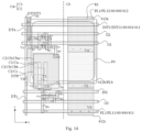
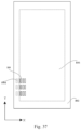
- Fig. 30 is a schematic diagram of a display substrate provided by an embodiment of the present disclosure.
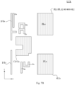
- the display substrate further includes a driving circuit CCT, the driving circuit CCT is located at one side of the display substrate, one sub-pixel 100 (sub-pixel 151) away from the driving circuit CCT has a first brightness L1; one sub-pixel 100 (sub-pixel 152) close to the driving circuit CCT has a second brightness L2, and the value range of
- Fig. 30 shows two driving circuits CCT located at the same side of the display substrate.
- the sub-pixel 151 and the sub-pixel 152 have different distances from the driving circuit CCT in the first direction Y, and the distance between the sub-pixel 151 and the sub-pixel 152 in the second direction X is not limited.
- the driving circuit CCT can be a driving integrated circuit (IC).
- the display substrate satisfies that the value range of (Xb1+Xb2)/WO is [0.08, 0.48], the problem of voltage drop and the problem of color shift can be solved; and the brightness difference can be reduced, and for example, the value range of
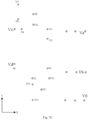
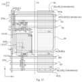
- Fig. 31 is a schematic diagram of a display substrate provided by an embodiment of the present disclosure.
- the display substrate further includes two driving circuits CCT, the two driving circuits CCT (driving circuit CCT1 and driving circuit CCT2) are located at opposite sides of the display region R01 of the display substrate, the sub-pixel 100 at the central axis of the display substrate has a third brightness L3, one sub-pixel 100 close to one of the two driving circuits CCT has a fourth brightness L4, and the value range of
- Fig. 31 shows the central axis CR extending in the second direction X.
- the extending direction of the central axis CR is the same as the extending direction of the driving circuit CCT.
- the central axis CR is located between the two driving circuits CCT.
- the sub-pixel 161 and the sub-pixel 162 have different distances from one of the two driving circuits CCT in the first direction Y, and the distance between the sub-pixel 161 and the sub-pixel 162 in the second direction X is not limited.
- the display substrate satisfies that the value range of (Xb1+Xb2)/WO is [0.08, 0.48], the problem of voltage drop and the problem of color shift can be solved; and the brightness difference can be reduced, and for example, the value range of
- the display substrate satisfies that the value range of
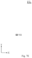
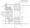
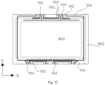
- Fig. 32 is a schematic diagram of a display substrate provided by an embodiment of the present disclosure.
- the display substrate includes a power bus 501, a power bus 502, an initialization bus 503, and an initialization bus 504.
- the power bus 501 is connected to the first power line PL1
- the power bus 502 is connected to the second power line PL2
- the initialization bus 503 is connected to the initialization line INT1
- the initialization bus 504 is connected to the initialization line INT2.
- the display substrate shown in Fig. 32 is provided with a driving circuit on the lower side thereof. It should be noted that the setting positions of the power bus 501, the power bus 502, the initialization bus 503, and the initialization bus 504 are not limited to those shown in the figure.
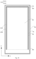
- Fig. 30-Fig. 32 show a display region R01.
- Fig. 33A is a plan view of a pixel defining layer in a display substrate provided by an embodiment of the present disclosure.
- Fig. 33B is a plan view of a pixel defining layer in a display substrate provided by an embodiment of the present disclosure. For example, as shown in Fig. 33A and Fig.
- the pixel defining layer PDL includes a plurality of first defining portions 301 and a plurality of second defining portions 302, the plurality of second defining portions 302 are arranged in the second direction X, each of the plurality of second defining portions 302 extends in the first direction Y, the plurality of first defining portions 301 are arranged as a plurality of groups 0301, each group of first defining portions 301 is located between two adjacent second defining portions 302, each of the plurality of first defining portions 301 extends in the second direction X, and the first defining portions 301 in each group are arranged in the first direction Y.
- a groove is formed between two adjacent second defining portions 302, and each groove extends in the first direction Y.
- the display substrate includes a plurality of columns of grooves.
- One column of grooves defines multiple pixel openings P0.
- the maximum height H1 from the first defining portion 301 to the planarization layer PLN is less than the maximum height H2 from the second defining portion 302 to the planarization layer PLN. That is, the thickness of the first defining portion 301 is less than the thickness of the second defining portion 302.
- Fig. 34 is a schematic diagram of a display substrate provided by an embodiment of the present disclosure.
- the base substrate BS includes a display region R01 and a peripheral region R02 located on at least one side of the display region R01.
- the orthographic projection of the part DT01 of the data line DT located in the display region R01 on the base substrate BS is located within the orthographic projection of the second defining portion 302 on the base substrate BS.
- the orthographic projection of the data line DT on the base substrate BS overlaps with the orthographic projection of the second defining portion 302 of the pixel defining layer PDL on the base substrate BS, so that the second defining portion 302 have a protrusion to facilitate the ink to flow into the pixel opening in the pixel defining layer during inkjet printing.
- the orthographic projection of the display region R01 on the base substrate BS overlaps with the orthographic projection of the pixel defining layer PDL on the base substrate BS.
- the orthographic projection of the pixel opening P0 of the pixel defining layer PDL on the base substrate BS falls within the orthographic projection of the display region R01 on the base substrate BS.
- Fig. 34 shows only two data lines DT.
- one second defining portion 302 can correspond to one data line, but it is not limited thereto.
- the pixel circuit is not limited to that shown in the given circuit diagram, and other suitable pixel circuits can be adopted; and the layout of the display substrate is not limited to that shown in the given layout diagram, and can be adjusted on the basis of the given layout diagram, or other layout manners can be adopted.
- a first defining portion 301 is arranged between two pixel openings P0 that are adjacent to each other in the first direction Y
- a second defining portion 302 is arranged between two pixel openings P0 that are adjacent to each other in the second direction X
- the first direction Y intersects with the second direction X.
- the thickness of the first defining portion 301 is H1
- the thickness of the second defining portion 302 is H2
- H1 is less than H2.
- Fig. 35 is an electron micrograph of a display substrate provided by an embodiment of the present disclosure.
- the slope angle of the bottom angle ⁇ 1 is in the range of 65-75 degrees; the slope angle ⁇ 2 is in the range of 45-55 degrees.
- the slope angle ⁇ 2 is a slope angle of the planarization layer PLN at the via hole VH in the case where a reference plane (at half the thickness of the planarization layer PLN) serves as the bottom surface.
- the bottom angle ⁇ 1 is an included angle between the planarization layer PLN at the bottom surface of the via hole VH and the structure below the planarization layer PLN.
- the display substrate further includes an insulating layer ISL;
- the light-emitting element 100b includes a first electrode E1, a second electrode E2, and a light-emitting functional layer FL located between the first electrode E1 and the second electrode E2; and the first electrode E1 of the light-emitting element 100b is connected to the pixel circuit 100a through the via hole VH penetrating the insulating layer ISL.
- the display substrate further includes an encapsulation layer EPS
- the encapsulation layer EPS is configured to encapsulate the light-emitting element 100b
- the encapsulation layer EPS includes a stack of an inorganic encapsulation film and an organic encapsulation film.
- the encapsulation layer EPS includes an inorganic encapsulation film EPS1, an organic encapsulation film EPS2, and an inorganic encapsulation film EPS3. It should be noted that the stacking order of the organic encapsulation film and the inorganic encapsulation film is not limited to that shown in the figure, nor is the structure of the encapsulation layer EPS limited to that shown in the figure.
- Fig. 36 is a schematic diagram of a display substrate provided by an embodiment of the present disclosure.
- the display substrate further includes a barrier dam 701
- an encapsulation adhesive 702 is provided at an outer side of the encapsulation layer EPS, and the encapsulation adhesive 702 plays a bonding role.
- Fig. 36 shows the encapsulation layer EPS with the boundary of the encapsulation layer EPS. As shown in Fig. 6 and Fig.
- the insulating layer ISL includes a planarization layer PLN
- the planarization layer PLN includes a first planarization portion PLN1 and a second planarization portion PLN2
- a groove GR is arranged between the first planarization portion PLN1 and the second planarization portion PLN2
- the barrier dam 701 is located at the periphery of the display region R01 of the display substrate
- the orthographic projection of the barrier dam 701 on the base substrate BS covers the orthographic projection of the groove GR on the base substrate BS, so as to alleviate or prevent water and oxygen from entering the display region along the planarization layer PLN, and avoid affecting the light-emitting elements in the display region R01.
- the orthographic projection of the barrier dam 701 on the base substrate BS may not cover the orthographic projection of the groove GR on the substrate BS.
- the minimum distance between the edge of the display region R01 and the edge of the peripheral region R02 ranges from 1 mm to 5 mm. That is, the size of the bezel ranges from 1 mm to 5 mm.
- the groove GR is a through hole penetrating the planarization layer PLN.
- the portion of the planarization layer PLN located at the inner side of the groove GR is the first planarization portion PLN1
- the portion of the planarization layer PLN located at the outer side of the groove GR is the second planarization portion PLN2.
- Fig. 36 shows the first planarization portion PLN1 with the boundary of the first planarization portion PLN1 and the second planarization portion PLN2 with the boundary of the second planarization portion PLN2.
- the number of grooves GR is not limited to one, and can be set as needed.
- the number of grooves GR depends on the narrow degree of narrow bezel. The narrower the bezel, the fewer the number of grooves GR. Of course, in some other embodiments, the groove GR may not be provided.
- the display substrate further includes a data line DT, a gate line G1, a gate line G2 and an initialization line INT1
- the pixel circuit 100a further includes a data writing transistor T1 and a reset transistor T2, the first electrode of the data writing transistor T1 is connected to the data line DT, the gate electrode of the driving transistor T3 is connected to the second electrode of the data writing transistor T1, the gate electrode of the data writing transistor T1 is connected to the gate line G1, the first electrode of the reset transistor T2 is connected to the initialization line INT1, the second electrode of the reset transistor T2 is connected to the gate electrode of the driving transistor T3, and the gate electrode of the reset transistor T2 is connected to the gate line G2.
- Fig. 37 is a schematic diagram of a display substrate provided by an embodiment of the present disclosure.
- Fig. 38 is a schematic circuit diagram of a dummy sub-pixel in a display substrate provided by an embodiment of the present disclosure.
- Fig. 39 is a layout diagram of a dummy pixel circuit in a display substrate provided by an embodiment of the present disclosure.
- a dummy sub-pixel 100d is arranged in the vicinity of an edge of the display substrate.
- Fig. 37 does not show all dummy sub-pixels nor all sub-pixels 100.
- the dummy sub-pixel 100d is located in the peripheral region R02, and the sub-pixel 100 is located in the display region R01.
- the dummy sub-pixel 100d does not emit light, and providing the dummy sub-pixel 100d can improve etching uniformity and improve the display quality.
- the dummy sub-pixel 100d is provided with a dummy driving transistor dT3 and a dummy reset transistor dT2, the dummy reset transistor dT2 is connected to the gate electrode of the dummy driving transistor dT3, and the dummy reset transistor dT2 is disconnected from the initialization line INT1, so as to reduce power consumption.
- the dummy sub-pixel 100d is provided to improve the etching uniformity, instead of realizing the luminescent function.
- the dummy sub-pixel 100d includes a dummy pixel circuit 100da and a dummy light-emitting element 100db. As shown in Fig.
- the composition of the dummy pixel circuit 100da can refer to the composition of the pixel circuit 100a
- the composition of the dummy light-emitting element 100db can refer to the composition of the light-emitting element 100b.
- the dummy pixel circuit 100da may have a disconnected line therein.
- the dummy pixel circuit 100da shown in Fig. 38 is illustrated by taking the example that the first electrode E1 of the dummy light-emitting element 100db is not connected to the node N2 (first electrode T3a of the dummy driving transistor dT3) and the dummy reset transistor dT2 is not connected to the initialization line INT1.
- dummy sub-pixel 100d not emit light.
- a bold cross in Fig. 38 indicates disconnection.
- a via hole may not be provided.
- the dummy sub-pixel 100d further includes a dummy data writing transistor dT1.
- Fig. 38 and Fig. 39 further show a dummy data line dDT.
- the dummy sub-pixel 100d further includes a dummy storage capacitor dCst.
- the components in the dummy sub-pixel 100d are given new reference numerals except the main components such as transistors and storage capacitors, etc., and the reference numerals of other components can refer to those in the sub-pixel 100.
- Fig. 40 is a schematic diagram of a display substrate provided by an embodiment of the present disclosure.
- the display substrate further includes a dummy data line dDT, the dummy data line dDT extends in the first direction Y, the dummy data line dDT and the data line DT are insulated from each other, the dummy sub-pixel 100d includes at least two dummy sub-pixels 100d that are adjacent to each other in the second direction X, and the dummy data lines dDT of the at least two dummy sub-pixels 100d are connected to each other.
- the dummy data line dDT is located in the peripheral region R02.
- the peripheral region R02 surrounds the display region R01.
- the dummy data line dDT is connected to a constant voltage terminal, so as to be configured to provide a constant voltage.
- the constant voltage terminal includes a terminal that provides the first voltage signal VDD, a terminal that provides the second voltage signal VSS, or a terminal that provides the initialization signal Vinit1.
- the dummy data line dDT is connected to the first power line PL1, the second power line PL2, or the initialization line INT1.
- the dummy data line dDT is connected to the constant voltage terminal, which is beneficial to reducing the resistance of the power line connected to the constant voltage terminal and improve the display quality.
- the display substrate further includes a first power line PL1
- the pixel circuit 100a further includes a light-emitting control transistor T5, the first electrode of the light-emitting control transistor T5 is connected to the first power line PL1, and the second electrode of the light-emitting control transistor T5 is connected to the second electrode of the driving transistor T3.
- the display substrate further includes a pixel defining layer PDL
- the pixel defining layer PDL includes a defining portion 300
- the pixel opening P0 is defined by the defining portion 300
- the light-emitting element 100b includes a first electrode E1 and a light-emitting functional layer FL
- the pixel defining layer PDL is configured to expose at least a part of the first electrode E1
- at least a part of film layers in the light-emitting functional layer FL covers the sidewall SW of the defining portion 300 (as shown in Fig. 6).
- Fig. 6 is illustrated by taking that the light-emitting functional layer FL is located in the pixel opening P0 as an example.
- the light-emitting functional layer FL can include a common layer, as shown in Fig. 45 .
- Fig. 41A is a schematic diagram of a display substrate provided by an embodiment of the present disclosure.
- the display substrate further includes a dummy pixel defining layer dPDL
- the dummy pixel defining layer dPDL includes a plurality of dummy defining portions d300 (second dummy defining portions d302) arranged in the second direction X
- the extending direction of the second dummy defining portion d302 is the same as the extending direction of the second defining portion 302
- the spacing W4 between two adjacent dummy defining portions d300 (second dummy defining portions d302) is greater than the spacing W3 between two adjacent second defining portions 302.
- FIG. 41A further shows a plurality of first dummy defining portions d301 extending in the second direction X. As shown in Fig. 41 , multiple first dummy defining portions d301 are provided between adjacent second dummy defining portions d302.
- Fig. 41A shows a display region R01 and a peripheral region R02.
- the spacing W4 is greater than the spacing W3, which is beneficial to the wiring of the peripheral region R02.
- the spacing W4 can be a maximum spacing, that is, the maximum spacing W4 between two adjacent dummy defining portions d300 is greater than the maximum spacing W3 between two adjacent second defining portions 302.
- the spacing W4 can be a minimum spacing, that is, the minimum spacing W4 between two adjacent dummy defining portions d300 is greater than the minimum spacing W3 between two adjacent second defining portions 302.
- Fig. 41A is illustrated by taking that three columns of dummy sub-pixels 100d are provided between two adjacent second dummy defining portions d302 as an example, but it is not limited to this case, and one column, two columns or more than three columns of dummy sub-pixels 100d can be provided between two adjacent second dummy defining portions d302. That is, at least one column of dummy sub-pixels 100d is provided between two adjacent second dummy defining portions d302.
- Fig. 41A takes that the peripheral region R02 is provided with the first dummy defining portion d301 extending in the second direction X as an example, but it is not limited to this case. In some embodiments, the peripheral region R02 may not be provided with the first dummy defining portion d301. In this case, the dummy pixel defining layer dPDL only includes the second dummy defining portion d302.
- the width W6 can be equal to the width W5.
- Fig. 42 is a schematic diagram of a display substrate provided by an embodiment of the present disclosure.
- the display substrate further includes a reset transistor T4, an initialization line INT2, and an initialization bus 504, the initialization bus 504 is arranged at the outer side of the display region R01 of the display substrate, the first electrode of the reset transistor T4 is connected to the initialization bus 504, the first electrode T4a of the reset transistor T4 is connected to the initialization bus 504 through the initialization line INT2, the second electrode T4b of the reset transistor T4 is connected to the light-emitting element 100b through the driving transistor T3, and the reset transistor T4 is connected to a row of sub-pixels 100.
- the number (a count) of reset transistors T4 is less than the number (a count) of sub-pixels 100.
- Fig. 42 is illustrated by taking that one row of sub-pixels corresponds to one reset transistor T4 as an example.
- the reset transistor T4 is located in the peripheral region R02.
- the initialization bus 504 is located in the peripheral region R02.
- Fig. 44 is a circuit diagram of a display substrate provided by an embodiment of the present disclosure. As shown in Fig. 44 , the number (a count) of light-emitting control transistors T5 of sub-pixels 100 in one row is less than the number (a count) of sub-pixels 100 in the row. For example, three sub-pixels 100 in one pixel PX are all connected to the same light-emitting control transistor T5.
- the embodiments of the present disclosure further provide a display substrate, which includes a base substrate BS and a plurality of sub-pixels 100 disposed on the base substrate BS.
- the sub-pixel 100 includes a pixel circuit 100a and a light-emitting element 100b, the pixel circuit 100a includes a driving transistor T3 and a storage capacitor Cst, the storage capacitor Cst includes a first electrode plate Ca and a second electrode plate Cb, the first electrode plate Ca of the storage capacitor Cst is connected to the gate electrode of the driving transistor T3, and the second electrode plate Cb of the storage capacitor Cst is connected to the first electrode of the driving transistor T3; the light-emitting element 100b is electrically connected to the pixel circuit 100a, the pixel circuit 100a is configured to drive the light-emitting element 100b, the sub-pixel 100 includes a pixel opening P0, the pixel opening P0 is configured to define a light-emitting
- the embodiments of the present disclosure further provide a display substrate, which includes a base substrate BS and a plurality of sub-pixels 100 disposed on the base substrate BS.
- the sub-pixel 100 includes a pixel circuit 100a and a light-emitting element 100b, the pixel circuit 100a includes a driving transistor T3 and a storage capacitor Cst, the storage capacitor Cst includes a first electrode plate Ca and a second electrode plate Cb, the first electrode plate Ca of the storage capacitor Cst is connected to the gate electrode of the driving transistor T3, and the second electrode plate Cb of the storage capacitor Cst is connected to the first electrode of the driving transistor T3; the light-emitting element 100b is electrically connected to the pixel circuit 100a, the pixel circuit 100a is configured to drive the light-emitting element 100b, the sub-pixel 100 includes a pixel opening P0, the pixel opening P0 is configured to define a light-emitting region of the sub-pixel 100, the orthographic projection of the storage capacitor Cst on the base substrate BS overlaps with the orthographic projection of the pixel opening P0 on the base substrate BS, the orthographic projection of the channel of the driving transistor T3 on the base
- the embodiments of the present disclosure further provide a display substrate, which includes a base substrate BS and a plurality of sub-pixels 100 disposed on the base substrate BS.
- the sub-pixel 100 includes a pixel circuit 100a and a light-emitting element 100b, the pixel circuit 100a includes a driving transistor T3 and a storage capacitor Cst, the storage capacitor Cst includes a first electrode plate Ca and a second electrode plate Cb, the first electrode plate Ca of the storage capacitor Cst is connected to the gate electrode of the driving transistor T3, and the second electrode plate Cb of the storage capacitor Cst is connected to the first electrode of the driving transistor T3; the light-emitting element 100b is electrically connected to the pixel circuit 100a, the pixel circuit 100a is configured to drive the light-emitting element 100b, the sub-pixel 100 includes a pixel opening P0, the pixel opening P0 is configured to define a light-emitting
- the embodiments of the present disclosure further provide a display substrate, which includes a base substrate BS and a plurality of sub-pixels 100 disposed on the base substrate BS.
- the sub-pixel 100 includes a pixel circuit 100a and a light-emitting element 100b, the pixel circuit 100a includes a driving transistor T3 and a storage capacitor Cst, the storage capacitor Cst includes a first electrode plate Ca and a second electrode plate Cb, the first electrode plate Ca of the storage capacitor Cst is connected to the gate electrode of the driving transistor T3, and the second electrode plate Cb of the storage capacitor Cst is connected to the first electrode of the driving transistor T3;
- the light-emitting element 100b is electrically connected to the pixel circuit 100a, the pixel circuit 100a is configured to drive the light-emitting element 100b, the sub-pixel 100 includes a pixel opening P0, the pixel opening P0 is configured to define a light-emitting region of the sub-pixel 100, the orthographic projection of the storage capacitor
- the first voltage signal VDD is 17V
- the second voltage signal VSS is 2V
- k0 2.8*E-07
- W 2 microns
- L 30 microns
- Uc 15V
- P k0*(W/L)*Uc
- P 2.8*E-07 watts.
- the above power consumption P is the power consumption of a single sub-pixel.
- different designs can be carried out to solve the power consumption matching problem of sub-pixels with different colors and reduce the power consumption of the whole panel.
- the power consumption of the red sub-pixel is less than the power consumption of the green sub-pixel
- the power consumption of the green sub-pixel is less than the power consumption of the blue sub-pixel, so as to solve the problem of three-color power consumption matching and reduce the power consumption of the whole panel.
- the display substrate can further satisfy the following relationship: a value range of (W*L+S2)*M1/M2 is [0.014, 0.133], S2 is the facing area between the second electrode plate Cb and the first electrode plate Ca, M1 is the number (a count) of pixel openings P0 in the display substrate, and M2 is the area of the display substrate, so as to facilitate the formation of a display substrate with better performance using inkjet printing technology
- a value range of (W*L+S2)*M1/M2 is [0.014, 0.133]
- a value range of S2/(W*L) is [2.82, 28.85]
- P k0*(W/L)*Uc.
- "*" in the formula represents the multiplication sign
- " / " is the division sign
- a range [Mx, My] represents greater than or equal to Mx and less than or equal to My
- Mx and My are numbers
- the numbers with E in [] are numerical values expressed by scientific counting method.
- Fig. 45 is a schematic diagram of a display substrate provided by an embodiment of the present disclosure.
- the light-emitting functional layer FL includes a hole injection layer HIL, a hole transport layer HTL, a light-emitting layer EML and an electron injection layer EIL, and the materials of the hole injection layer HIL, the hole transport layer HTL and the light-emitting layer EML are located in the pixel opening defined by the pixel definition layer PDL, while the electron injection layer EIL is a common layer.
- Fig. 45 further shows that the display substrate includes a light extraction layer (capping layer) CPL to facilitate the improvement of light extraction efficiency.
- the hole injection layer HIL and the hole transport layer HTL can adopt a gradient doping mode, or can adopt a stack arrangement of single layers.
- the structure of the display substrate provided by the embodiment of the present disclosure is not limited to that shown in Fig. 45 .
- Fig. 46 is a schematic diagram of a brightness test of a display substrate provided by an embodiment of the present disclosure.
- the display substrate includes a display region R01 and a peripheral region R02, and the sub-pixels are located in the display region R01.
- a plurality of test points are selected from the display region.
- Nine test points are selected in Fig. 46 .
- the brightness of each test point can be measured.
- Fig. 46 shows that the sub-pixels can be divided into a plurality of sub-pixel groups PG, and Fig. 46 shows a sub-pixel group PG1, a sub-pixel group PG2, and a sub-pixel group PG3.
- each sub-pixel group PG can correspond to one or more rows of sub-pixels.
- each sub-pixel group PG can correspond to one or more columns of sub-pixels.
- the first to third test points are three test points at different positions of the sub-pixel group PG1
- the fourth to sixth test points are three test points at different positions of the sub-pixel group PG2
- the seventh to ninth test points are three test points at different positions of the sub-pixel group PG3.
- the brightness of the sub-pixels in each sub-pixel group PG can be the average of the brightness at the test points corresponding to the sub-pixel group PG.
- the brightness of the sub-pixels in the sub-pixel group PG1 is the average of the brightness values of the first test point, the second test point, and the third test point
- the brightness of the sub-pixels in the sub-pixel group PG2 is the average of the brightness values of the fourth test point, the fifth test point, and the sixth test point
- the brightness of the sub-pixels in the sub-pixel group PG3 is the average of the brightness values of the seventh test point, the eighth test point, and the ninth test point.
- the test point at the middle position can be in the middle of the test points close to the boundary of the display region.
- the distance between the second test point and the first test point is equal to the distance between the second test point and the third test point.
- the distance between the fifth test point and the fourth test point is equal to the distance between the fifth test point and the sixth test point
- the distance between the eighth test point and the seventh test point is equal to the distance between the eighth test point and the ninth test point.
- the distance between the fourth test point and the first test point is equal to the distance between the fourth test point and the seventh test point
- the distance between the fifth test point and the second test point is equal to the distance between the fifth test point and the eighth test point
- the distance between the sixth test point and the third test point is equal to the distance between the sixth test point and the ninth test point, but it is not limited to this case.
- Fig. 46 shows the length Ly and width Lx of the display region R01.
- the distance Lx0 between the test point and the boundary of the display region R01 in the second direction X is greater than or equal to Lx/10
- the distance Ly0 between the test point and the boundary of the display region R01 in the first direction Y is greater than or equal to Ly/10.
- the data line DT includes a data line DT1, a data line DT2, and a data line DT3.
- the data line DT1 provides a data signal for the first sub-pixel 101
- the data line DT2 provides a data signal for the second sub-pixel 102
- the data line DT3 provides a data signal for the third sub-pixel 103.
- the first power line PL1 and the initialization line INT1 of the pixel circuit 100a are formed by using two conductive pattern layers, parts of the first power line PL1 and parts of the initialization line INT1 extending in the first direction Y are all formed in segments. Parts of the first power line PL1 and parts of the initialization line INT1 extending in the second direction X are all located in the second conductive pattern layer LY2.
- the signal connection line 412 includes at least one of a first power connection line PL12 and an initialization connection line INT12.
- the display substrate further includes a data line DT
- the data line DT is configured to provide a data voltage to the sub-pixel 100
- the orthographic projection of at least one of the signal connection line 412 and the data line DT on the base substrate BS overlaps with the orthographic projection of the pixel opening P0 of at least one sub-pixel among the plurality of sub-pixels 100 on the base substrate BS.
- the flatter the bottom surface of the pixel opening P0 of the sub-pixel 100 i.e., the first electrode E1 of the light-emitting element
- the more color shift can be alleviated or avoided, and the better the display effect of the display substrate.
- the part, directly below the pixel opening P0, of the data line DT or the signal connection line 412 located in the second conductive pattern layer LY2 can play a role of leveling to improve the display quality.
- the signal connection line 412 includes at least one of a part of the first power line PL1 extending in the first direction Y and a part of the initialization line extending in the first direction Y.
- the signal connection line 412 and the signal transmission line 411 are connected through a via hole.
- the display substrate further includes a signal transmission line 512, the signal transmission line 512 is configured to provide a voltage signal to the sub-pixel 100, the signal transmission line 512 extends in the second direction X, and the orthographic projection of the signal transmission line 512 on the base substrate BS overlaps with the orthographic projection of the pixel opening P0 of at least one sub-pixel among the plurality of sub-pixels 100 on the base substrate BS. Therefore, it is beneficial to the longitudinal flow leveling of ink during inkjet printing, and alleviating the color shift of the up and down viewing angles.
- the signal transmission line 512 includes at least one of a gate line G1, a gate line G2, and a part of the initialization line INT11 extending in the second direction X.
- At least one of the reset transistor T4 and the light-emitting control transistor T5 may not be provided in the pixel circuit 100a, and the structure of the pixel circuit 100a is not limited to that shown in the figure, and can be provided as needed.
- the orthographic projection of the pixel opening P0 of the sub-pixel on the base substrate does not overlap with the orthographic projection of the via hole VH on the base substrate, which is illustrated as an example. But in some other embodiments, the orthographic projection of the pixel opening P0 of the sub-pixel on the base substrate can overlap with the orthographic projection of the via hole VH on the base substrate.
- the design of the backplane film layer such as the design of elements in the second conductive pattern layer, can be adapted to the pixel openings of the sub-pixels with different sizes, so as to improve the flatness of the light-emitting functional layer and further alleviate the color shift of the left and right viewing angles of the display substrate.
- the color shift can be alleviated and the display quality can be improved by adjusting the size of the pixel opening of the sub-pixel, adjusting the size of the third electrode plate of the storage capacitor, and overlapping the opening with the signal line.
- the thickness of an element refers to the size of the element in the direction perpendicular to the base substrate.
- the size of the pixel opening P0 of the first sub-pixel 101 in the second direction X is in the range of 28-36 microns
- the size of the pixel opening P0 of the second sub-pixel 102 in the second direction X is in the range of 30-38 microns
- the size of the pixel opening P0 of the third sub-pixel 103 in the second direction X is in the range of 68-74 microns.
- the size of the pixel opening P0 of the sub-pixel 100 is not limited to this case, and can be determined as needed.
- the insulating layer ISL includes a passivation layer PVX and a planarization layer PLN
- the material of the passivation layer PVX includes an inorganic insulating material
- the material of the planarization layer PLN includes an organic insulating material.
- the thickness of the planarization layer PLN is in the range of 3-7 microns.
- the display substrate provided by the embodiment of the present disclosure can alleviate the color shift between the left and right viewing angles to less than 0.015.
- the display substrate provided by the embodiment of the present disclosure by overlapping the pixel opening of the sub-pixel with the signal connection line (designing the position of the longitudinal wiring), the color shift problem of the second sub-pixel (green sub-pixel) is obviously improved, and the deviation between the left and right 60-degree viewing angle is small.
- the thickness of the planarization layer PLN is thicker than that of an evaporation product.
- the thickness of the planarization layer can be effectively reduced through the backplane design.
- the width of the via hole VH is reduced to significantly alleviate the color shift.
- the thickness of the planarization layer is in the range of 3-7 microns.
- the insulating layer ISL shown in Fig. 6 can be formed of an inorganic material layer, or an organic material layer, or an organic material layer and an organic material layer.
- the preparation of via holes in the insulating layer ISL is not limited to one-time manufacture. In order to reduce the diameter of via hole, the form of preparing sleeve holes by multiple-time manufacture is adopted, which is beneficial to the flatness of the light-emitting functional layer and further alleviating the color shift.
- the ratio of the diameter of the uppermost via hole to the width of the pixel opening of the sub-pixel is less than 0.3.
- the width of the pixel opening of the sub-pixel can refer to the maximum size of the pixel opening of the sub-pixel in the second direction X.
- the gate line G1 can be referred to as a first gate line
- the gate line G2 can be referred to as a second gate line
- the gate line G4 can be referred to as a third gate line
- the reset transistor T2 can be referred to as a first reset transistor
- the reset transistor T4 can be referred to as a second reset transistor.
- the display substrate further includes a data line, a first gate line, a second gate line, a third gate line, a first power line, a first initialization line, and a second initialization line;
- the data line is configured to provide a data voltage to the pixel circuit
- the first gate line is configured to provide a scan signal to the pixel circuit
- the second gate line is configured to provide a first reset control signal to the pixel circuit
- the third gate line is configured to provide a second reset control signal to the pixel circuit
- the first power line is configured to provide a first voltage signal to the pixel circuit
- the first initialization line is configured to provide a first initialization signal to the pixel circuit
- the second initialization line is configured to provide a second initialization signal to the pixel circuit
- the pixel circuit further includes a data writing transistor, a first reset transistor, and a second reset transistor, the first electrode of the data writing transistor is connected to the data line, the gate electrode of the data writing transistor is connected to the first gate line, and the second electrode
- the gate line G5 can be referred to as a fourth gate line
- the display substrate further includes a fourth gate line and a light-emitting control transistor
- the fourth gate line is configured to provide a light-emitting control signal to the light-emitting control transistor
- the second electrode of the driving transistor is connected to the first power line through the light-emitting control transistor.
- the active layer of each transistor can include a source region, a drain region, and a channel between the source region and the drain region.
- the channel has semiconductor characteristics; the source region and the drain region are located on both sides of the channel and can be doped with impurities, so they have conductivity and can serve as the first and second electrodes of the transistor respectively.
- One of the first and second electrodes of the transistor is the source electrode, and the other of the first and second electrodes of the transistor is the drain electrode.
- the material of the semiconductor layer (semiconductor pattern) used to manufacture the active layer can include oxide semiconductor, organic semiconductor, amorphous silicon, or polysilicon, etc.
- the oxide semiconductor includes metal oxide semiconductor (such as indium gallium zinc oxide (IGZO)), and the polysilicon includes low-temperature polysilicon or high-temperature polysilicon, etc., which is not limited in the embodiment of the present disclosure.
- IGZO indium gallium zinc oxide
- the above-mentioned source region and drain region can be regions doped with N-type impurities or P-type impurities, which is not limited by the embodiment of the present disclosure.
- the base substrate BS, the buffer layer BL, the barrier layer BR, the gate insulating layer GI, the interlayer insulating layer ILD, the planarization layer PLN, and the pixel defining layer PDL are all made of insulating materials.
- the base substrate BS includes a flexible material, such as polyimide, etc., but it is not limited thereto.
- At least one of the buffer layer BF, the barrier layer BR, the gate insulating layer GI, and the interlayer insulating layer ILD is made of an inorganic insulating material or an organic insulating material.
- the inorganic insulating material includes silicon oxide, silicon nitride, silicon oxynitride, etc.
- the organic insulating material includes resin, but is not limited thereto.
- the pixel defining layer PDL and the planarization layer PLN can be made of an organic material, and for example, the organic material includes resin, but is not limited thereto.
- both the first conductive pattern layer LY1 and the second conductive pattern layer LY2 are made of metal materials, and the specific materials can be determined as needed.
- the material of the first conductive pattern layer LY1 includes molybdenum (Mo).
- the material of the second conductive pattern layer LY2 includes titanium (Ti) and aluminum (Al), and a structure in which three layers of Ti/Al/Ti are stacked can be adopted, but it is not limited to this case.
- the material of the first electrode E1 of the light-emitting element includes a conductive material, such as at least one of silver (Ag) or indium tin oxide (ITO), but is not limited thereto.
- the first electrode E1 of the light-emitting element has a structure in which three layers of ITO/Ag/ITO are stacked, but it is not limited thereto.
- the material of the first electrode E1 of the light-emitting element includes aluminum (Al) and tungsten oxide (WOx).
- the first electrode E1 includes a stack of an aluminum layer and an tungsten oxide layer, and the aluminum layer is closer to the base substrate than the tungsten oxide layer.
- the material of the second electrode E2 of the light-emitting element includes a conductive material, such as silver (Ag), but is not limited thereto.
- the patterns of each single layer and the via holes can be manufactured by a patterning process.
- forming a specific pattern includes forming a thin film, forming a photoresist pattern on the thin film, and patterning the thin film with the photoresist pattern as a mask to form the specific pattern.
- the first conductive pattern layer LY1, the second conductive pattern layer LY2, the first electrode layer LY3, the third conductive pattern layer LY4, and the via holes in the insulating layer can be formed by this method.
- a semiconductor pattern can be formed first, and then doped by a doping process, so that the semiconductor pattern is formed into an active layer including a channel, a source region, and a drain region, an insulating layer is formed on the active layer, a first conductive pattern layer LY1 is formed on the insulating layer, and subsequent film layers are formed in turn.
- each sub-pixel 101 can further include other numbers of transistors or other numbers of capacitors, and the pixel circuit works under the control of the data signal transmitted through the data line, the gate scan signal transmitted through the gate line, and the light-emitting control signal provided by the light-emitting control signal line to drive the light-emitting element to emit light, so as to realize operations, such as display, etc.
- the number of thin film transistors and the number of capacitors included in the pixel circuit are not limited in the embodiment of the present disclosure.
- the display substrate provided by the embodiment of the present disclosure can adopt any other suitable layout diagram, and the wiring mode is not limited to that shown in the drawings.
- At least one embodiment of the present disclosure provides a display device, which includes any one of the display substrates described above.
- the display device can be a large-sized display device, and at least one film layer in the light-emitting functional layer is manufactured by adopting inkjet printing process.
- the display device can be an organic light-emitting diode display device.
- the display device can be any product or component including organic light-emitting diode display and having display function, such as a TV, a digital camera, a mobile phone, a watch, a tablet computer, a notebook computer, a navigator, etc.
Landscapes
- Engineering & Computer Science (AREA)
- Microelectronics & Electronic Packaging (AREA)
- Physics & Mathematics (AREA)
- Geometry (AREA)
- Computer Hardware Design (AREA)
- General Physics & Mathematics (AREA)
- Theoretical Computer Science (AREA)
- Electroluminescent Light Sources (AREA)
- Devices For Indicating Variable Information By Combining Individual Elements (AREA)
- Transforming Electric Information Into Light Information (AREA)
Applications Claiming Priority (1)
| Application Number | Priority Date | Filing Date | Title |
|---|---|---|---|
| PCT/CN2022/132588 WO2024103344A1 (zh) | 2022-11-17 | 2022-11-17 | 显示基板和显示装置 |
Publications (2)
| Publication Number | Publication Date |
|---|---|
| EP4580360A1 true EP4580360A1 (de) | 2025-07-02 |
| EP4580360A4 EP4580360A4 (de) | 2025-10-29 |
Family
ID=91083450
Family Applications (1)
| Application Number | Title | Priority Date | Filing Date |
|---|---|---|---|
| EP22965526.1A Pending EP4580360A4 (de) | 2022-11-17 | 2022-11-17 | Anzeigesubstrat und anzeigevorrichtung |
Country Status (6)
| Country | Link |
|---|---|
| US (1) | US20250113705A1 (de) |
| EP (1) | EP4580360A4 (de) |
| JP (1) | JP2025536514A (de) |
| KR (1) | KR20250110321A (de) |
| CN (1) | CN118370027B (de) |
| WO (1) | WO2024103344A1 (de) |
Families Citing this family (2)
| Publication number | Priority date | Publication date | Assignee | Title |
|---|---|---|---|---|
| WO2024113102A1 (zh) * | 2022-11-28 | 2024-06-06 | 京东方科技集团股份有限公司 | 显示基板和显示装置 |
| KR20250156541A (ko) * | 2024-04-25 | 2025-11-03 | 엘지디스플레이 주식회사 | 디스플레이 장치 |
Family Cites Families (13)
| Publication number | Priority date | Publication date | Assignee | Title |
|---|---|---|---|---|
| TW493282B (en) * | 2000-04-17 | 2002-07-01 | Semiconductor Energy Lab | Self-luminous device and electric machine using the same |
| JP2007134482A (ja) * | 2005-11-10 | 2007-05-31 | Toppan Printing Co Ltd | 薄膜トランジスタ装置およびその製造方法、並びに、それを使用した薄膜トランジスタアレイおよび薄膜トランジスタディスプレイ |
| JP5422991B2 (ja) * | 2008-12-24 | 2014-02-19 | ソニー株式会社 | 表示装置および表示装置の製造方法 |
| KR102086404B1 (ko) * | 2013-09-04 | 2020-03-09 | 엘지디스플레이 주식회사 | 유기전계발광 소자, 그 제조 방법 및 유기전계발광 표시장치 |
| KR102457466B1 (ko) * | 2015-02-02 | 2022-10-21 | 삼성디스플레이 주식회사 | 유기 발광 표시 장치 |
| US11877482B2 (en) * | 2019-10-29 | 2024-01-16 | Hefei Boe Joint Technology Co., Ltd. | Display substrate and method for manufacturing the same, driving method and display device |
| US11997890B2 (en) * | 2019-11-20 | 2024-05-28 | Chengdu Boe Optoelectronics Technology Co., Ltd. | Display substrate and method for manufacturing the same, and display device |
| CN111785759B (zh) * | 2020-07-17 | 2025-04-29 | 武汉华星光电半导体显示技术有限公司 | 显示面板及显示装置 |
| CN113516947B (zh) * | 2021-04-22 | 2023-01-17 | 武汉天马微电子有限公司 | 显示面板和显示装置 |
| CN113823639B (zh) * | 2021-09-09 | 2024-02-27 | 武汉天马微电子有限公司 | 显示面板及显示装置 |
| CN114093918B (zh) * | 2021-11-17 | 2025-10-21 | 京东方科技集团股份有限公司 | 显示面板及显示装置 |
| CN114155814B (zh) * | 2021-12-09 | 2022-12-06 | 武汉天马微电子有限公司 | 像素驱动电路及显示面板、显示装置 |
| CN115633521B (zh) * | 2022-11-17 | 2023-07-18 | 北京京东方技术开发有限公司 | 显示基板和显示装置 |
-
2022
- 2022-11-17 WO PCT/CN2022/132588 patent/WO2024103344A1/zh not_active Ceased
- 2022-11-17 CN CN202280004344.2A patent/CN118370027B/zh active Active
- 2022-11-17 KR KR1020257020146A patent/KR20250110321A/ko active Pending
- 2022-11-17 JP JP2025518340A patent/JP2025536514A/ja active Pending
- 2022-11-17 US US18/560,169 patent/US20250113705A1/en active Pending
- 2022-11-17 EP EP22965526.1A patent/EP4580360A4/de active Pending
Also Published As
| Publication number | Publication date |
|---|---|
| WO2024103344A9 (zh) | 2025-03-06 |
| KR20250110321A (ko) | 2025-07-18 |
| JP2025536514A (ja) | 2025-11-07 |
| EP4580360A4 (de) | 2025-10-29 |
| CN118370027A (zh) | 2024-07-19 |
| US20250113705A1 (en) | 2025-04-03 |
| WO2024103344A1 (zh) | 2024-05-23 |
| CN118370027B (zh) | 2026-01-27 |
Similar Documents
| Publication | Publication Date | Title |
|---|---|---|
| CN115633521B (zh) | 显示基板和显示装置 | |
| US20240431163A1 (en) | Display substrate and display apparatus | |
| CN111863929B (zh) | 显示基板及其制备方法、显示装置 | |
| EP4152401B1 (de) | Anzeigesubstrat und herstellungsverfahren dafür sowie anzeigevorrichtung | |
| US12400607B2 (en) | Display substrate and display device | |
| US11910670B2 (en) | Display substrate and manufacturing method thereof, and compensating method for wire load | |
| US20250143111A1 (en) | Display Substrate and Display Apparatus | |
| EP4580360A1 (de) | Anzeigesubstrat und anzeigevorrichtung | |
| WO2024113102A1 (zh) | 显示基板和显示装置 | |
| US20240251611A1 (en) | Display Substrate, Preparing Method Therefor, and Display Apparatus | |
| CN115132815A (zh) | 显示基板及显示装置 | |
| US12426457B2 (en) | Display substrate and manufacturing method thereof, and display device | |
| US20240237433A1 (en) | Display panel and display device | |
| US12142210B2 (en) | Display panel and display apparatus | |
| US20240381712A1 (en) | Display Substrate and Display Apparatus | |
| WO2023123239A9 (zh) | 显示面板和电子设备 | |
| CN117322163A (zh) | 显示基板及显示装置 | |
| WO2021168731A1 (zh) | 显示基板及其制备方法、显示装置 | |
| CN223415235U (zh) | 显示基板和显示装置 | |
| US20250234727A1 (en) | Display substrate, display panel and display device | |
| WO2025246694A1 (zh) | 显示面板和显示装置 | |
| US20240389420A1 (en) | Display substrate, preparation method therefor, and display apparatus | |
| US20240324373A1 (en) | Display Substrate and Display Apparatus |
Legal Events
| Date | Code | Title | Description |
|---|---|---|---|
| STAA | Information on the status of an ep patent application or granted ep patent |
Free format text: STATUS: THE INTERNATIONAL PUBLICATION HAS BEEN MADE |
|
| PUAI | Public reference made under article 153(3) epc to a published international application that has entered the european phase |
Free format text: ORIGINAL CODE: 0009012 |
|
| STAA | Information on the status of an ep patent application or granted ep patent |
Free format text: STATUS: REQUEST FOR EXAMINATION WAS MADE |
|
| 17P | Request for examination filed |
Effective date: 20250328 |
|
| AK | Designated contracting states |
Kind code of ref document: A1 Designated state(s): AL AT BE BG CH CY CZ DE DK EE ES FI FR GB GR HR HU IE IS IT LI LT LU LV MC ME MK MT NL NO PL PT RO RS SE SI SK SM TR |
|
| A4 | Supplementary search report drawn up and despatched |
Effective date: 20250930 |
|
| RIC1 | Information provided on ipc code assigned before grant |
Ipc: H10K 59/121 20230101AFI20250924BHEP |