EP4580352A2 - Mikro-led, mikro-led-array-tafel und herstellungsverfahren dafür - Google Patents
Mikro-led, mikro-led-array-tafel und herstellungsverfahren dafür Download PDFInfo
- Publication number
- EP4580352A2 EP4580352A2 EP25169570.6A EP25169570A EP4580352A2 EP 4580352 A2 EP4580352 A2 EP 4580352A2 EP 25169570 A EP25169570 A EP 25169570A EP 4580352 A2 EP4580352 A2 EP 4580352A2
- Authority
- EP
- European Patent Office
- Prior art keywords
- semiconductor layer
- type semiconductor
- ion implantation
- fence
- micro led
- Prior art date
- Legal status (The legal status is an assumption and is not a legal conclusion. Google has not performed a legal analysis and makes no representation as to the accuracy of the status listed.)
- Withdrawn
Links
Images


Classifications
-
- H—ELECTRICITY
- H10—SEMICONDUCTOR DEVICES; ELECTRIC SOLID-STATE DEVICES NOT OTHERWISE PROVIDED FOR
- H10H—INORGANIC LIGHT-EMITTING SEMICONDUCTOR DEVICES HAVING POTENTIAL BARRIERS
- H10H20/00—Individual inorganic light-emitting semiconductor devices having potential barriers, e.g. light-emitting diodes [LED]
- H10H20/80—Constructional details
- H10H20/81—Bodies
- H10H20/816—Bodies having carrier transport control structures, e.g. highly-doped semiconductor layers or current-blocking structures
- H10H20/8162—Current-blocking structures
-
- H—ELECTRICITY
- H10—SEMICONDUCTOR DEVICES; ELECTRIC SOLID-STATE DEVICES NOT OTHERWISE PROVIDED FOR
- H10H—INORGANIC LIGHT-EMITTING SEMICONDUCTOR DEVICES HAVING POTENTIAL BARRIERS
- H10H20/00—Individual inorganic light-emitting semiconductor devices having potential barriers, e.g. light-emitting diodes [LED]
- H10H20/01—Manufacture or treatment
- H10H20/011—Manufacture or treatment of bodies, e.g. forming semiconductor layers
- H10H20/013—Manufacture or treatment of bodies, e.g. forming semiconductor layers having light-emitting regions comprising only Group III-V materials
- H10H20/0137—Manufacture or treatment of bodies, e.g. forming semiconductor layers having light-emitting regions comprising only Group III-V materials the light-emitting regions comprising nitride materials
-
- H—ELECTRICITY
- H10—SEMICONDUCTOR DEVICES; ELECTRIC SOLID-STATE DEVICES NOT OTHERWISE PROVIDED FOR
- H10H—INORGANIC LIGHT-EMITTING SEMICONDUCTOR DEVICES HAVING POTENTIAL BARRIERS
- H10H20/00—Individual inorganic light-emitting semiconductor devices having potential barriers, e.g. light-emitting diodes [LED]
- H10H20/80—Constructional details
- H10H20/81—Bodies
- H10H20/819—Bodies characterised by their shape, e.g. curved or truncated substrates
-
- H—ELECTRICITY
- H10—SEMICONDUCTOR DEVICES; ELECTRIC SOLID-STATE DEVICES NOT OTHERWISE PROVIDED FOR
- H10H—INORGANIC LIGHT-EMITTING SEMICONDUCTOR DEVICES HAVING POTENTIAL BARRIERS
- H10H20/00—Individual inorganic light-emitting semiconductor devices having potential barriers, e.g. light-emitting diodes [LED]
- H10H20/80—Constructional details
- H10H20/83—Electrodes
- H10H20/831—Electrodes characterised by their shape
-
- H—ELECTRICITY
- H10—SEMICONDUCTOR DEVICES; ELECTRIC SOLID-STATE DEVICES NOT OTHERWISE PROVIDED FOR
- H10H—INORGANIC LIGHT-EMITTING SEMICONDUCTOR DEVICES HAVING POTENTIAL BARRIERS
- H10H20/00—Individual inorganic light-emitting semiconductor devices having potential barriers, e.g. light-emitting diodes [LED]
- H10H20/80—Constructional details
- H10H20/84—Coatings, e.g. passivation layers or antireflective coatings
-
- H—ELECTRICITY
- H10—SEMICONDUCTOR DEVICES; ELECTRIC SOLID-STATE DEVICES NOT OTHERWISE PROVIDED FOR
- H10H—INORGANIC LIGHT-EMITTING SEMICONDUCTOR DEVICES HAVING POTENTIAL BARRIERS
- H10H29/00—Integrated devices, or assemblies of multiple devices, comprising at least one light-emitting semiconductor element covered by group H10H20/00
- H10H29/10—Integrated devices comprising at least one light-emitting semiconductor component covered by group H10H20/00
- H10H29/14—Integrated devices comprising at least one light-emitting semiconductor component covered by group H10H20/00 comprising multiple light-emitting semiconductor components
- H10H29/142—Two-dimensional arrangements, e.g. asymmetric LED layout
-
- H10W90/00—
-
- H—ELECTRICITY
- H10—SEMICONDUCTOR DEVICES; ELECTRIC SOLID-STATE DEVICES NOT OTHERWISE PROVIDED FOR
- H10H—INORGANIC LIGHT-EMITTING SEMICONDUCTOR DEVICES HAVING POTENTIAL BARRIERS
- H10H20/00—Individual inorganic light-emitting semiconductor devices having potential barriers, e.g. light-emitting diodes [LED]
- H10H20/01—Manufacture or treatment
- H10H20/011—Manufacture or treatment of bodies, e.g. forming semiconductor layers
- H10H20/017—Etching
-
- H—ELECTRICITY
- H10—SEMICONDUCTOR DEVICES; ELECTRIC SOLID-STATE DEVICES NOT OTHERWISE PROVIDED FOR
- H10H—INORGANIC LIGHT-EMITTING SEMICONDUCTOR DEVICES HAVING POTENTIAL BARRIERS
- H10H20/00—Individual inorganic light-emitting semiconductor devices having potential barriers, e.g. light-emitting diodes [LED]
- H10H20/01—Manufacture or treatment
- H10H20/011—Manufacture or treatment of bodies, e.g. forming semiconductor layers
- H10H20/018—Bonding of wafers
-
- H—ELECTRICITY
- H10—SEMICONDUCTOR DEVICES; ELECTRIC SOLID-STATE DEVICES NOT OTHERWISE PROVIDED FOR
- H10H—INORGANIC LIGHT-EMITTING SEMICONDUCTOR DEVICES HAVING POTENTIAL BARRIERS
- H10H20/00—Individual inorganic light-emitting semiconductor devices having potential barriers, e.g. light-emitting diodes [LED]
- H10H20/01—Manufacture or treatment
- H10H20/011—Manufacture or treatment of bodies, e.g. forming semiconductor layers
- H10H20/019—Removal of at least a part of a substrate on which semiconductor layers have been formed
-
- H—ELECTRICITY
- H10—SEMICONDUCTOR DEVICES; ELECTRIC SOLID-STATE DEVICES NOT OTHERWISE PROVIDED FOR
- H10H—INORGANIC LIGHT-EMITTING SEMICONDUCTOR DEVICES HAVING POTENTIAL BARRIERS
- H10H20/00—Individual inorganic light-emitting semiconductor devices having potential barriers, e.g. light-emitting diodes [LED]
- H10H20/80—Constructional details
- H10H20/81—Bodies
- H10H20/822—Materials of the light-emitting regions
- H10H20/824—Materials of the light-emitting regions comprising only Group III-V materials, e.g. GaP
- H10H20/825—Materials of the light-emitting regions comprising only Group III-V materials, e.g. GaP containing nitrogen, e.g. GaN
Definitions
- the present disclosure generally relates to light emitting diode, and more particularly, to a micro light emitting diode (LED), a micro LED array panel, and a manufacturing method thereof.
- LED micro light emitting diode
- micro LEDs Inorganic micro pixel light emitting diodes, also referred to as micro light emitting diodes, micro LEDs or ⁇ -LEDs, are of increasing importance because of their use in various applications including self-emissive micro-displays, visible light communications, and optogenetics.
- the micro LEDs exhibit higher output performance than conventional LEDs due to better strain relaxation, improved light extraction efficiency, and uniform current spreading.
- the micro LEDs also exhibit improved thermal effects, fast response rate, larger work temperature range, higher resolution, color gamut and contrast, and lower power consumption, and can be operated at higher current density compared with conventional LEDs.
- the inorganic micro LEDs are conventionally III - V group epitaxial layers formed as multiple mesas.
- a space is formed between the adjacent micro LEDs in the conventional micro LEDs structures to avoid carriers in the epitaxial layer spreading from one mesa to an adjacent mesa.
- the space which is formed between the adjacent micro LEDs can reduce an active light emitting area and decrease light extraction efficiency. If there is no space between the adjacent micro LEDs, the active light emitting area would be increased and the carriers in the epitaxial layer would spread laterally to the adjacent mesa, which reduces the light emitting efficiency of the micro LED. Furthermore, if there is no space formed between the adjacent mesas, cross talk will be produced between the adjacent micro LEDs, which would interfere with LEDs operation.
- Embodiments of the present disclosure provide micro LED array panel.
- the micro LED array panel includes a first type semiconductor layer formed in the micro LED array panel; a first type cap layer formed on the first type semiconductor layer; a light emitting layer formed on the first type cap layer; a second type cap layer formed on the light emitting layer; and a second type semiconductor layer formed on the second type cap layer; wherein the first type is P type and the second type is N type; and the first type semiconductor layer includes multiple mesa structures, multiple trenches and multiple ion implantation fences separated from the mesa structures by the trenches; wherein a top surface of the ion implantation fence is lower than or aligned with a top surface of the first type semiconductor layer; and the ion implantation fences are formed around the trench and between adjacent type mesa structures; wherein an electrical resistance of the ion implantation fence is higher than an electrical resistance of the mesa structure.
- Embodiments of the present disclosure provide a method for manufacturing a micro LED.
- the method includes providing an epitaxial structure, wherein the epitaxial structure includes a first type semiconductor layer, a first type cap layer, a light emitting layer, a second type cap layer, and a second type semiconductor layer sequentially from top to bottom; patterning the first type semiconductor layer to form a mesa structure, a trench, and a fence; depositing a bottom contact on the mesa structure; and performing an ion implantation process into the fence to form an ion implantation fence.
- Embodiments of the present disclosure provide a micro LED.
- the micro LED includes a first type semiconductor layer; a first type cap layer formed on the first type semiconductor layer; a light emitting layer formed on the first type cap layer; a second type cap layer formed on the light emitting layer; and a second type semiconductor layer formed on the second type cap layer; wherein the first type is P type and the second type is N type; the second type semiconductor layer includes a mesa structure, a trench, and an ion implantation fence separated from the mesa structure; wherein a bottom surface of the ion implantation fence is not lower than a bottom surface of the second type semiconductor layer; and the ion implantation fence is formed around the trench and the trench is formed around the mesa structure; wherein an electrical resistance of the second ion implantation fence is higher than an electrical resistance of the second mesa structure.
- Embodiments of the present disclosure provide micro LED array panel.
- the micro LED array panel includes a first type semiconductor layer formed in the micro LED array panel; a first type cap layer formed on the first type semiconductor layer; a light emitting layer formed on the first type cap layer; a second type cap layer formed on the light emitting layer; and a second type semiconductor layer formed on the second type cap layer; wherein the first type is P type and the second type is N type; the second type semiconductor layer includes multiple mesa structures, multiple trenches and multiple ion implantation fences separated from the mesa structures by the trenches; wherein a bottom surface of the ion implantation fence is higher than or aligned with a bottom surface of the second type semiconductor layer; and the ion implantation fences are formed around the trench and between adjacent mesa structures; wherein an electrical resistance of the ion implantation fence is higher than an electrical resistance of the mesa structure.
- Embodiments of the present disclosure provide a method for manufacturing a micro LED.
- the method includes providing an epitaxial structure, wherein the epitaxial structure includes a first type semiconductor layer, a first type cap layer, a light emitting layer, a second type cap layer, and a second type semiconductor layer sequentially from top to bottom; bonding the epitaxial structure with an integrated circuit (IC) backplane; patterning the second type semiconductor layer to form a mesa structure, a trench, and a fence; depositing a top contact on the mesa structure; performing an ion implantation process into the fence; depositing a top conductive layer on a top surface of the second type semiconductor layer, on a top contact, and in the trench.
- IC integrated circuit
- Embodiments of the present disclosure provide a micro LED.
- the micro LED includes a first type semiconductor layer; a first type cap layer formed on the first type semiconductor layer; a light emitting layer formed on the first type cap layer; a second type cap layer formed on the light emitting layer; and a second type semiconductor layer formed on the second type cap layer; wherein the first type is P type and the second type is N type; and the first type semiconductor layer includes a first mesa structure, a first trench, and a first ion implantation fence separated from the first mesa structure; wherein a top surface of the first ion implantation fence is lower than or aligned with a top surface of the first type semiconductor layer; and the second type semiconductor layer includes a second mesa structure, a second trench, and a second ion implantation fence separated from the second mesa structure; wherein a bottom surface of the second ion implantation fence is higher than or aligned with a bottom surface of the second type semiconductor layer; and the first ion implantation
- Embodiments of the present disclosure provide micro LED array panel.
- the micro LED array panel includes a first type semiconductor layer formed in the micro LED array panel; a first type cap layer formed on the first type semiconductor layer; a light emitting layer formed on the first type cap layer; a second type cap layer formed on the light emitting layer; and a second type semiconductor layer, formed on the second type cap layer; wherein the first type is P type and the second type is N type; the first type semiconductor layer includes multiple first mesa structures, multiple first trenches and multiple first ion implantation fences separated from the first mesa structures by the first trenches; a top surface of the first ion implantation fence is lower than or aligned with a top surface of the first type semiconductor layer; the first ion implantation fences are formed around the first trench and between adjacent first type mesa structures; wherein an electrical resistance of the first ion implantation fence is higher than an electrical resistance of the first mesa structure; and the second type semiconductor layer includes multiple second mesa structures, multiple second
- Embodiments of the present disclosure provide a method for manufacturing a micro LED.
- the method includes a process I comprising patterning a first type semiconductor layer; and implanting first ions into the first type semiconductor layer; and a process II comprising patterning a second type semiconductor layer; and implanting second ions into the second type semiconductor layer.
- the present disclosure provides a micro LED which can avoid nonradiative recombination at sidewalls of a mesa according to a structure of a semiconductor layer and continuously formed light emitting layer. Furthermore, compared with conventional micro LEDs, a space between adjacent mesas can be decreased largely due to an ion implantation fence. Therefore, the integration level of the micro LEDs in a chip is increased and the active light emitting efficiency is improved. Furthermore, the micro LED provided by the present disclosure can also increase the active light emitting area and improve the image quality.
- the micro LED includes a first type semiconductor layer 110, a first type cap layer 114, a light emitting layer 130, a second type cap layer 124, and a second type semiconductor layer 120.
- the light emitting layer 130 is formed on the first type cap layer 114 over the first type semiconductor layer 110
- the second type semiconductor layer 120 is formed on the second type cap layer 124 over the light emitting layer 130.
- the thickness of the first type semiconductor layer 110 is greater than the thickness of the second type semiconductor layer 120.
- a conductive type of the first type semiconductor layer 110 is different from a conductive type of the second type semiconductor layer 120.
- the conductive type of the first type semiconductor layer 110 is P type and the conductive type of the second type semiconductor layer 120 is N type.
- the conductive type of the second type semiconductor layer 120 is P type and the conductive type of the first type semiconductor layer 110 is N type.
- a material of the first type semiconductor layer 110 can be selected from one or more of p-GaAs, p-GaP, p-AlInP, p-GaN, p-InGaN, or p- AlGaN.
- the material of the second type semiconductor layer 120 can be selected from one or more of n-GaAs, n-AlInP, n-GaInP, n-AlGaAs, n-AlGaInP, n-GaN, n-InGaN, or n-AlGaN.
- a conductive type of the first type cap layer 114 is the same as the conductive type of the first type semiconductor layer 110 and a conductive type of the second type cap layer 124 is the same as the second type semiconductor layer 120.
- the first type semiconductor layer 110 includes a mesa structure 111, a trench 112 and an ion implantation fence 113.
- the ion implantation fence 113 is separated from the mesa structure 111 by the trench 112.
- the trench 112 and the ion implantation fence 113 are annular around the mesa structure 111.
- the ion implantation fence 113 includes a light absorption material for absorbing light from the mesa structure 111.
- a conductive type of the light absorption material is the same as the conductive type of the first semiconductor layer 110.
- the light absorption material is selected from one or more of p-GaAs, p-GaP, p-AlInP, p-GaN, p-InGaN, or p-AlGaN.
- the ion implantation fence 113 is formed at least by implanting ions into the first type semiconductor layer 110.
- the ion type implanted into the first type semiconductor layer 110 is selected from one or more of H, N, Ar, Kr, Xe, As, 0, C, P, B, Si, S, Cl, or F.
- the width of the ion implantation fence 113 is not greater than 50% of the diameter of the mesa structure 111. In some embodiments, the width of the ion implantation fence 113 is not greater than I0% of the diameter of the mesa structure 111. Preferably, the width of the ion implantation fence 113 is not greater than 200 nm, the diameter of the mesa structure 111 is not greater than 2500 nm, and the thickness of the first type semiconductor layer 110 is not greater than 300 nm.
- the width of the trench 112 is not greater than 50% of the diameter of the mesa structure 111. In some embodiments, the width of the trench 112 is not greater than I0% of the diameter of the mesa structure 111. Preferably, the width of the first trench 112 is not greater than 200 nm.
- the top surface of the ion implantation fence 113 is not higher than the top surface of the first type semiconductor layer 110. Therefore, the ion implantation fence 113 can contact the first type cap layer 114 but cannot contact the light emitting layer 130.
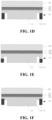
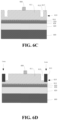
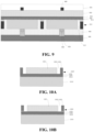
- the top surface of the ion implantation fence 113 can be formed at any position within the first type semiconductor layer 110. As shown in FIG. 1A , the trench 112 extends up through the first type semiconductor layer 110 to the first type cap layer 114. A top surface of the trench 112 is aligned with a top surface of the first type semiconductor layer 110. A top surface of the ion implantation fence 113 is aligned with the top surface of the trench 112. FIG.
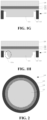
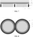
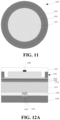
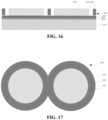
- FIG. 2 is a structural diagram showing a bottom view of the first exemplary micro LED as shown in FIG. 1A , according to some embodiments of the present disclosure.
- FIG. 2 shows a bottom view of the first type semiconductor layer 110 in which the ion implantation fence 113 is separated from the mesa structure 111 by the trench 112.
- the ion implantation fence 113 is formed around the trench and the trench is formed around the mesa structure 111. Since the trench extends up through the first type semiconductor layer 110 to the first type cap layer 114, the first type cap layer 114 can be seen through the trench in the bottom view.
- the top surface of the ion implantation fence 113 is lower than the top surface of the trench 112. Additionally, in some embodiments, the trench 112 extends up through the first type semiconductor layer 110 and enters into an interior of the first type cap layer 114. In some embodiments, the trench 112 extends up through the first type semiconductor layer 110 and the first type cap layer 114 and further reaches the light emitting layer 130. In some embodiments, the trench 112 extends up through the first type semiconductor layer 110 and the first type cap layer 114, further extends into an interior of the light emitting layer 130. In some embodiments, the trench 112 extends up through the first type semiconductor layer 110, the first type cap layer 114 and the light emitting layer 130.
- the trench 112 extends up through the first type semiconductor layer 110, the first type cap layer 114 and the light emitting layer 130, further extends up into an interior of the second type cap layer 124. Furthermore, in some embodiments, the trench 112 extends up through the first type semiconductor layer 110, the first type cap layer 114, the light emitting layer 130 and the second type cap layer 124, and further extends up into an interior of the second type semiconductor layer 120.
- the trench 112 does not extend up through the first type semiconductor layer 110.
- the top surface of the ion implantation fence 113 is higher than the top surface of the trench 112.
- the top surface of the ion implantation fence 113 is aligned with the top surface of the trench 112.
- the top surface of the ion implantation fence 113 is lower than the top surface of the trench 112.
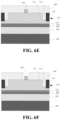
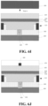
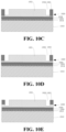
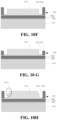
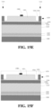
- the bottom surface of the ion implantation fence 113 can be formed at any position. Preferably, the bottom surface of the ion implantation fence 113 is aligned with the bottom surface of the first type semiconductor layer 110. Referring to FIG. 1F , in some embodiments, the bottom surface of the ion implantation fence 113 is higher than the bottom surface of the first type semiconductor layer 110. Referring to FIG. 1G , in some embodiments, the bottom surface of the ion implantation fence 113 is lower than the bottom surface of the first type semiconductor layer 110.
- the mesa structure 111 includes a stair structure 111a. In some embodiment, the mesa structure 111 can have one or more stair structures.
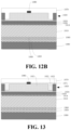
- FIG. 3 is a structural diagram showing a side sectional view of another variant of the first exemplary micro LED, according to some embodiments of the present disclosure.
- the micro LED further includes a bottom isolation layer 140 filled in the trench 112.
- the material of the bottom isolation layer 140 is selected from one or more of SiO 2 , SiNx, Al 2 O 3 , AlN, HfO 2 , TiO 2 , or ZrO 2 .
- an integrated circuit (IC) backplane 190 is formed under the first type semiconductor layer 110 and is electrically connected with the first type semiconductor layer 110 via a connection structure 150.
- the connection structure 150 is a connection pillar.
- the micro LED further includes a bottom contact 160.
- the bottom contact 160 is formed at the bottom of the first type semiconductor layer 110.
- An upper surface of the connection structure 150 is connected with a bottom contact 160 and the bottom surface of the connection structure 150 is connected with the IC backplane 190.
- the micro LED further includes a top contact 180 and a top conductive layer 170.
- the top contact 180 is formed on the top of the second type semiconductor layer 120.
- the top conductive layer 170 is formed on the top of the second type semiconductor layer 120 and the top contact 180.
- the conductive type of the top contact 180 is the same as the conductive type of the second type semiconductor layer 120.
- the conductive type of the second type semiconductor layer 120 is N type and the conductive type of the top contact 180 is N type.
- the conductive type of the second type semiconductor layer 120 is P type and the conductive type of the top contact 180 is P type.
- the top contact 180 is made of metal or metal alloy, such as, AuGe, AuGeNi, etc.
- the top contact 180 is used for forming an ohmic contact between the top conductive layer 170 and the second type semiconductor layer 120, to optimize the electrical properties of the micro LED.
- the diameter of the top contact 180 is about 20-50 nm and the thickness of the top contact 180 is about 10-20nm.
- a dielectric layer is formed between the top conductive layer 170 and the second type semiconductor layer 120.
- FIG. 4 is a structural diagram showing a side sectional view of another variant of the first exemplary micro LED, according to some embodiments of the present disclosure.
- the connection structure 150 is a metal bonding layer for bonding the micro LED with the IC backplane 190.
- the bottom contact 160 is a bottom contact layer in this variant.
- FIG. 5 shows a flow chart of a method 500 for manufacturing the first exemplary micro LED, for example, the micro LED shown in FIG. 3 , according some embodiments of the present disclosure.
- the method 500 for manufacturing the micro LED includes steps 501-510.
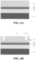
- FIG. 6A to FIG. 6J are structural diagrams showing a side sectional view of a micro LED manufacturing process at each step (i.e., steps 501-510) corresponding to the method 500 shown in FIG. 5 , according to some embodiments of the present disclosure.
- an epitaxial structure is provided.
- the epitaxial structure includes a first type semiconductor layer 610, a first type cap layer 614, a light emitting layer 630, a second type cap layer 624 and a second type semiconductor layer 620 sequentially from top to bottom.
- the epitaxial structure is grown on a substrate 600.
- the substrate 600 can be GaN, GaAs, etc.
- step 502 referring to FIG. 6B , the first type semiconductor layer 610 is patterned to form a mesa structure 611, a trench 613, and a fence 613'.
- the first type semiconductor layer 610 is etched and the etching is stopped above the first type cap layer 614 to avoid the light emitting layer 630 being etched in the patterning process.
- the bottom of the trench 612 does not reach the light emitting layer 630.
- the first type semiconductor layer 610 is etched by a conventional dry etching process, such as, a plasma etching process, which can be understood be those skilled in the field.
- step 503 referring to FIG. 6C , a bottom contact 660 is deposited on the mesa structure 611.
- a first protective mask (not shown) is used to protect an area where the bottom contact 660 will not be formed. Then, the material of the bottom contact 660 is deposited on the first protective mask and on the first type semiconductor layer 610 by a conventional vapor deposition process, such as a physical vapor deposition process or a chemical vapor deposition process. After the deposition process, the first protective mask is removed from the first type semiconductor layer 610 and the material on the first protective mask is also removed with the first protective mask to form the bottom contact 660 on the mesa structure 611.
- a top conductive layer 1570 is deposited on the top of the second type semiconductor layer 1520 and on the top contact 1580, and fills in the trench 1522.
- the top conductive layer 1570 is deposited by a conventional physical vapor deposition process.
- an IC backplane 1890 is formed under the first type semiconductor layer 1810 and is electrically connected with the first type semiconductor layer 1810 via a connection structure 1850.
- the micro LED array panel further includes a bottom contact 1860 formed at the bottom of the first type semiconductor layer 1810.
- the connection structure 1850 can be a metal bonding layer for bonding the micro LED with the IC backplane 1890.
- the bottom contact 1860 is a bottom contact layer. Further details of the IC backplane 1890, the bottom contact 1860, and the connection structure 1850 can be understood by also referring to FIG. 13 , which will not be further described here.
- the bottom surface of the trench is aligned with the top surface of the second type cap layer 1824. That is, the bottom surface of the trench contacts the second type cap layer 1824.
- the bottom surface of the trench is higher than the top surface of the second type cap layer 1824. That is, the bottom surface of the trench does not contact the second type cap layer 1824.
- micro LEDs and the ion implantation fence in the micro LED array panel can be understood by also referring to the micro LEDs as shown in FIGs. 10A-10H , which will not be further described here.
- the micro LED array panel shown in FIGs. 18A-18C can be manufactured by the method of manufacturing the micro LED 1400 as shown in FIG. 14 , which will not be further described here.
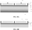
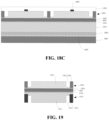
- FIG. 19 is a structural diagram showing a side sectional view of a variant of a third exemplary micro LED, according to some embodiments of the present disclosure.
- the micro LED at least includes a first type semiconductor layer 1910, a first type cap layer 1914, a light emitting layer 1930, a second type cap layer 1924, and a second type semiconductor layer 1920.
- a conductive type of the first type semiconductor layer 1910 is different from a conductive type of the second type semiconductor layer 1920.
- the conductive type of the first type semiconductor layer 1910 is P type
- the conductive type of the second type semiconductor layer 1920 is N type.
- a conductive type of the first type cap layer 1914 is the same as the conductive type of the first type semiconductor layer 1910 and a conductive type of the second type cap layer 1924 is the same as the second type semiconductor layer 1920.
- the first type semiconductor layer 1910 includes a first mesa structure 1911, a first trench 1912, and a first ion implantation fence 1913 separated from the first mesa structure 1911.
- the second type semiconductor layer 1920 includes a second mesa structure 1921, a second trench 1922, and a second ion implantation fence 1923 separated from the second mesa structure 1921.
- the center of the first mesa structure 1911 is aligned with the center of the second mesa structure 1921
- the center of the first trench 1912 is aligned with the center of the second trench 1922
- the center of the first ion implantation fence 1913 is aligned with the center of the second ion implantation fence 1923.
- the second mesa structure 1921 can have one or multiple stair structures, as shown in FIG. 10H .
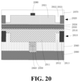
- FIG. 20 is a structural diagram showing a side sectional view of another variant of the third exemplary micro LED, according to some embodiments of the present disclosure.
- the micro LED further includes a bottom isolation layer 2040 filled in a first trench 2012.
- the material of the bottom isolation layer 2040 is one or more of SiO 2 , SiNx, Al 2 O 3 , AlN, HfO 2 , TiO 2 , or ZrO 2 .
- An IC backplane 2090 is formed under a first type semiconductor layer 2010 and is electrically connected with the first type semiconductor layer 2010 via a connection structure 2050.
- the connection structure 2050 is a connection pillar.
- the micro LED further includes a bottom contact 2060 formed at the bottom of the first type semiconductor layer 2010. Further detail of the bottom isolation layer 2040, the IC backplane 2090, the connection structure 2050, and the bottom contact 2060 can be found by referring to the description for Embodiment 1, which will not be further described here.
- the micro LED further includes a top contact 2080 and a top conductive layer 2070.
- the top contact 2080 is formed on the top of a second type semiconductor layer 2020.
- the top conductive layer 2070 is formed on the top of the second type semiconductor layer 2020 and the top contact 2080 and fills in the second trench 2022. Further details regarding the top contact 2080 and the top conductive layer 2070 can be found by referring to the description for Embodiment 2, which will not be further described here.
- a dielectric layer 1071 as shown in FIG. 13 can be formed on the surface of the second type semiconductor layer 2020, which can be understood by referring to the description of FIG. 13 and will not be further described here.
- micro LED shown in FIG. 20 including a first ion implantation fence 2013 and a second ion implantation fence 2023, can be found by referring to the description for Embodiment 1 and Embodiment 2, which will not be further described here.
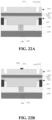
- FIG. 21 shows a flow chart of a method 2100 for manufacturing the third exemplary micro LED, according some embodiments of the present disclosure.
- the method 2100 includes at least Process I and Process II.
- Process I the first type semiconductor layer is patterned, and then ions are implanted into the first type semiconductor layer, to form a first ion implantation fence.
- step 2104 referring to FIG. 6D , an ion implantation process is performed into the fence 613'.
- step 2107 referring to FIG. 6G , metal material 650' is deposited on the whole substrate 600.
- step 2109 referring to FIG. 6I , the connection pillar 650 is bonded with the IC backplane 690, and the substructure 600 is removed.
- FIGs. 22A-22D are structural diagrams showing a side sectional view of the micro LED manufacturing process at steps 2110-2113 of the method 2100 shown in FIG. 21 , according to some embodiments of the present disclosure.
- a second type semiconductor layer 2220 is patterned to form a mesa structure 2221, a trench 2222, and a fence 2223'.
- a top conductive layer 2270 is deposited on the top of the second type semiconductor layer 2220 and on the top contact 2280, and in the trench 2222.
- a micro LED array panel is further provided according to some embodiments of the present disclosure.
- the micro LED array panel includes a plurality of micro LEDs as described above and shown in FIGs. 19 and 20 . These micro LEDs can be arranged in an array in the micro LED array panel.
- the first type semiconductor layer 2310 includes multiple first mesa structures 2311, multiple first trenches 2312, and multiple first ion implantation fences 2313 separated from the first mesa structures via the first trenches 2312.
- the top surface of the first ion implantation fence 2313 is lower than the top surface of the first type semiconductor layer 2310.
- a bottom view of the micro LED array panel without an IC backplane is similar to the bottom view shown in FIG. 8 .
- the first ion implantation fences 2313 are formed around the first trenches 2312 and between the adjacent first type mesa structures.
- the electrical resistance of the first ion implantation fence 2313 is higher than the electrical resistance of the first mesa structure.
- the first ion implantation fence 2313 is formed around the first trench 2312 and the first trench 2312 is formed around the first mesa structure.
- the second type semiconductor layer 2320 includes multiple second mesa structures 2321, multiple second trenches 2322, and multiple second ion implantation fences 2323 separated from the second mesa structures 2321 via the second trenches 2322.
- the bottom surface of the second ion implantation fence 2323 is higher than the bottom surface of the second type semiconductor layer 2320.
- a top view of the micro LED array panel is similar to the top view shown in FIG. 17 in that the second ion implantation fences 2323 is formed around the second trench 2322 and between the adjacent second mesa structures 2321.
- the electrical resistance of the second ion implantation fence 2323 is higher than the electrical resistance of the second mesa structure 2321.
- the second ion implantation fence 2323 is formed around the second trench 2322 and the second trench 2322 is formed around the second mesa structure 2321.
- the space between the adjacent sidewalls of the second mesa structure 2321 is not greater than 600 nm.
- the width of the second ion implantation fence 2323 is not greater than 50% of the diameter of the second mesa structure 2321.
- the width of the second ion implantation fence 2423 is not greater than 10% of the diameter of the second mesa structure 2421.
- the width of the second ion implantation fence 2323 is not greater than 200 nm.
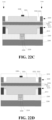
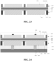
- FIG. 24 is a structural diagram showing a side sectional view of adjacent ones of the micro LED in FIG. 20 , in a micro LED array panel, according to some embodiments of the present disclosure.
- the micro LED array panel further includes a bottom isolation layer 2440 filled in a first trench 2412.
- the material of the bottom isolation layer 2440 is one or more of SiO 2 , SiNx, Al 2 O 3 , AlN, HfO 2 , TiO 2 , or ZrO 2 .
- an IC backplane 2490 is formed under a first type semiconductor layer 2410 and is electrically connected with the first type semiconductor layer 2410 via a connection structure 2450.
- micro LED in the micro LED array panel can be found by reference to the above described micro LEDs, which will not be further described here.
- the method of manufacturing the micro LED array panel at least includes manufacturing a micro LED. Details of manufacturing the micro LED can be found by reference to the description of steps 501-509 in the Embodiment 1 and the description of steps 1403-1406 in the Embodiment 2, which will not be further described here.
- a micro lens can be further formed on or above the top of the second type semiconductor layer, such as on the top surface of the top conductive layer, which can be understood by those skilled in the field.
- the micro LED herein has a very small volume.
- the micro LED may be an organic LED or an inorganic LED.
- the micro LED can be applied in a micro LED array panel.
- the light emitting area of the micro LED array panel is very small, such as 1 mm x 1 mm, 3 mm x 5 mm. In some embodiments, the light emitting area is the area of the micro LED array in the micro LED array panel.
- the micro LED array panel includes one or more micro LED arrays that form a pixel array in which the micro LEDs are pixels, such as a 1600 x 1200, 680 x 480, or 1920x1080 pixel array.
- the diameter of the micro LED is in the range of about 200 nm - 2 ⁇ m.
- An IC backplane is formed at the back surface of the micro LED array and is electrically connected with the micro LED array. The IC backplane acquires signals such as image data from outside via signal lines to control corresponding micro LEDs to emit light or not.
- the term "or" encompasses all possible combinations, except where infeasible. For example, if it is stated that a database may include A or B, then, unless specifically stated otherwise or infeasible, the database may include A, or B, or A and B. As a second example, if it is stated that a database may include A, B, or C, then, unless specifically stated otherwise or infeasible, the database may include A, or B, or C, or A and B, or A and C, or Band C, or A and B and C.
Landscapes
- Led Devices (AREA)
- Engineering & Computer Science (AREA)
- Power Engineering (AREA)
- Microelectronics & Electronic Packaging (AREA)
- Led Device Packages (AREA)
- Physics & Mathematics (AREA)
- Condensed Matter Physics & Semiconductors (AREA)
- General Physics & Mathematics (AREA)
- Computer Hardware Design (AREA)
Priority Applications (1)
| Application Number | Priority Date | Filing Date | Title |
|---|---|---|---|
| EP25169570.6A EP4580352A2 (de) | 2022-01-31 | 2022-01-31 | Mikro-led, mikro-led-array-tafel und herstellungsverfahren dafür |
Applications Claiming Priority (3)
| Application Number | Priority Date | Filing Date | Title |
|---|---|---|---|
| PCT/CN2022/075284 WO2023142142A1 (en) | 2022-01-31 | 2022-01-31 | Micro led, micro led array panel and manufacuturing method thereof |
| EP22922966.1A EP4473577A4 (de) | 2022-01-31 | 2022-01-31 | Mikro-led, mikro-led-array-tafel und herstellungsverfahren dafür |
| EP25169570.6A EP4580352A2 (de) | 2022-01-31 | 2022-01-31 | Mikro-led, mikro-led-array-tafel und herstellungsverfahren dafür |
Related Parent Applications (1)
| Application Number | Title | Priority Date | Filing Date |
|---|---|---|---|
| EP22922966.1A Division EP4473577A4 (de) | 2022-01-31 | 2022-01-31 | Mikro-led, mikro-led-array-tafel und herstellungsverfahren dafür |
Publications (1)
| Publication Number | Publication Date |
|---|---|
| EP4580352A2 true EP4580352A2 (de) | 2025-07-02 |
Family
ID=87432557
Family Applications (5)
| Application Number | Title | Priority Date | Filing Date |
|---|---|---|---|
| EP25170111.6A Withdrawn EP4565038A3 (de) | 2022-01-31 | 2022-01-31 | Mikro-led, mikro-led-array-tafel und herstellungsverfahren dafür |
| EP22922966.1A Pending EP4473577A4 (de) | 2022-01-31 | 2022-01-31 | Mikro-led, mikro-led-array-tafel und herstellungsverfahren dafür |
| EP25170170.2A Withdrawn EP4583670A3 (de) | 2022-01-31 | 2022-01-31 | Mikro-led, mikro-led-array-tafel und herstellungsverfahren dafür |
| EP25169570.6A Withdrawn EP4580352A2 (de) | 2022-01-31 | 2022-01-31 | Mikro-led, mikro-led-array-tafel und herstellungsverfahren dafür |
| EP25170210.6A Withdrawn EP4580351A2 (de) | 2022-01-31 | 2022-01-31 | Mikro-led, mikro-led-array-tafel und herstellungsverfahren dafür |
Family Applications Before (3)
| Application Number | Title | Priority Date | Filing Date |
|---|---|---|---|
| EP25170111.6A Withdrawn EP4565038A3 (de) | 2022-01-31 | 2022-01-31 | Mikro-led, mikro-led-array-tafel und herstellungsverfahren dafür |
| EP22922966.1A Pending EP4473577A4 (de) | 2022-01-31 | 2022-01-31 | Mikro-led, mikro-led-array-tafel und herstellungsverfahren dafür |
| EP25170170.2A Withdrawn EP4583670A3 (de) | 2022-01-31 | 2022-01-31 | Mikro-led, mikro-led-array-tafel und herstellungsverfahren dafür |
Family Applications After (1)
| Application Number | Title | Priority Date | Filing Date |
|---|---|---|---|
| EP25170210.6A Withdrawn EP4580351A2 (de) | 2022-01-31 | 2022-01-31 | Mikro-led, mikro-led-array-tafel und herstellungsverfahren dafür |
Country Status (7)
| Country | Link |
|---|---|
| US (1) | US20230246126A1 (de) |
| EP (5) | EP4565038A3 (de) |
| JP (1) | JP2025502550A (de) |
| KR (1) | KR20240141202A (de) |
| CN (1) | CN118661272A (de) |
| TW (1) | TWI883382B (de) |
| WO (1) | WO2023142142A1 (de) |
Families Citing this family (6)
| Publication number | Priority date | Publication date | Assignee | Title |
|---|---|---|---|---|
| WO2023142141A1 (en) * | 2022-01-31 | 2023-08-03 | Jade Bird Display (Shanghai) Company | Micro led, micro led array panel and manufacuturing method thereof |
| WO2025134553A1 (ja) * | 2023-12-20 | 2025-06-26 | ソニーセミコンダクタソリューションズ株式会社 | 発光装置および画像表示装置 |
| WO2025217787A1 (en) * | 2024-04-16 | 2025-10-23 | Jade Bird Display (shanghai) Limited | Micro led array and micro led display panel |
| WO2025217794A1 (en) * | 2024-04-16 | 2025-10-23 | Jade Bird Display (shanghai) Limited | Micro led array and micro led display panel |
| WO2025217793A1 (en) * | 2024-04-16 | 2025-10-23 | Jade Bird Display (shanghai) Limited | Micro led array and micro led display panel |
| WO2025217788A1 (en) * | 2024-04-16 | 2025-10-23 | Jade Bird Display (shanghai) Limited | Micro led array and micro led display panel |
Family Cites Families (18)
| Publication number | Priority date | Publication date | Assignee | Title |
|---|---|---|---|---|
| JP3233569B2 (ja) * | 1996-03-22 | 2001-11-26 | シャープ株式会社 | 半導体発光素子 |
| US6255129B1 (en) * | 2000-09-07 | 2001-07-03 | Highlink Technology Corporation | Light-emitting diode device and method of manufacturing the same |
| US8263422B2 (en) * | 2010-04-26 | 2012-09-11 | Varian Semiconductor Equipment Associates, Inc. | Bond pad isolation and current confinement in an LED using ion implantation |
| US8658513B2 (en) * | 2010-05-04 | 2014-02-25 | Varian Semiconductor Equipment Associates, Inc. | Isolation by implantation in LED array manufacturing |
| US8664027B2 (en) * | 2011-02-11 | 2014-03-04 | Varian Semiconductor Associates, Inc. | LED mesa sidewall isolation by ion implantation |
| US9625647B2 (en) * | 2014-01-29 | 2017-04-18 | The University Of Connecticut | Optoelectronic integrated circuit |
| CN104009135A (zh) * | 2014-06-11 | 2014-08-27 | 海迪科(南通)光电科技有限公司 | 新型阵列led高压芯片及其制备方法 |
| US10418519B2 (en) * | 2015-12-22 | 2019-09-17 | Apple Inc. | LED sidewall processing to mitigate non-radiative recombination |
| WO2020000184A1 (zh) * | 2018-06-26 | 2020-01-02 | 苏州晶湛半导体有限公司 | 半导体结构及其制造方法 |
| JP7398818B2 (ja) * | 2018-08-10 | 2023-12-15 | ビジョンラボ コーポレーション | 流体トランスファーシステムおよびマイクロled装置の製造方法 |
| CN110957399B (zh) * | 2018-09-26 | 2021-04-30 | 中国科学院苏州纳米技术与纳米仿生研究所 | 半导体光电子器件的制作方法 |
| EP3667721A1 (de) * | 2018-12-10 | 2020-06-17 | IMEC vzw | Verfahren zur herstellung einer optischen vorrichtung |
| CN111477726A (zh) * | 2019-05-08 | 2020-07-31 | 伊乐视有限公司 | 用于流体组装的平面表面贴装微型led及其制备方法 |
| CN110993758B (zh) * | 2019-10-31 | 2020-12-22 | 华灿光电(苏州)有限公司 | 微型发光二极管的显示阵列及其制作方法 |
| TW202543464A (zh) * | 2020-04-21 | 2025-11-01 | 大陸商上海顯耀顯示科技有限公司 | 具反射元件之發光二極體晶片結構 |
| US12113091B2 (en) * | 2020-05-05 | 2024-10-08 | Raysolve Optoelectronics (Suzhou) Company Limited | Full color light emitting diode structure and method for manufacturing the same |
| CN112768574B (zh) * | 2021-04-08 | 2021-06-18 | 度亘激光技术(苏州)有限公司 | 半导体结构的形成方法 |
| CN215578594U (zh) * | 2021-06-18 | 2022-01-18 | 京东方科技集团股份有限公司 | 一种微发光二极管芯片及显示装置 |
-
2022
- 2022-01-31 EP EP25170111.6A patent/EP4565038A3/de not_active Withdrawn
- 2022-01-31 CN CN202280090592.3A patent/CN118661272A/zh active Pending
- 2022-01-31 JP JP2024544952A patent/JP2025502550A/ja not_active Withdrawn
- 2022-01-31 EP EP22922966.1A patent/EP4473577A4/de active Pending
- 2022-01-31 EP EP25170170.2A patent/EP4583670A3/de not_active Withdrawn
- 2022-01-31 WO PCT/CN2022/075284 patent/WO2023142142A1/en not_active Ceased
- 2022-01-31 KR KR1020247029188A patent/KR20240141202A/ko active Pending
- 2022-01-31 EP EP25169570.6A patent/EP4580352A2/de not_active Withdrawn
- 2022-01-31 EP EP25170210.6A patent/EP4580351A2/de not_active Withdrawn
-
2023
- 2023-01-30 US US18/161,426 patent/US20230246126A1/en not_active Abandoned
- 2023-01-30 TW TW112103117A patent/TWI883382B/zh active
Also Published As
| Publication number | Publication date |
|---|---|
| KR20240141202A (ko) | 2024-09-25 |
| EP4565038A2 (de) | 2025-06-04 |
| TW202347811A (zh) | 2023-12-01 |
| TWI883382B (zh) | 2025-05-11 |
| CN118661272A (zh) | 2024-09-17 |
| EP4580351A2 (de) | 2025-07-02 |
| EP4583670A3 (de) | 2025-07-30 |
| WO2023142142A1 (en) | 2023-08-03 |
| EP4473577A1 (de) | 2024-12-11 |
| JP2025502550A (ja) | 2025-01-24 |
| EP4583670A2 (de) | 2025-07-09 |
| EP4565038A3 (de) | 2025-07-30 |
| EP4473577A4 (de) | 2025-11-19 |
| US20230246126A1 (en) | 2023-08-03 |
Similar Documents
| Publication | Publication Date | Title |
|---|---|---|
| EP4580352A2 (de) | Mikro-led, mikro-led-array-tafel und herstellungsverfahren dafür | |
| US20230246130A1 (en) | Micro-led, micro-led array panel and manufacturing method thereof | |
| US20230246131A1 (en) | Micro-led, micro-led array panel and manufacturing method thereof | |
| EP4518616A2 (de) | Mikro-led, mikro-led-array-tafel und herstellungsverfahren dafür |
Legal Events
| Date | Code | Title | Description |
|---|---|---|---|
| PUAI | Public reference made under article 153(3) epc to a published international application that has entered the european phase |
Free format text: ORIGINAL CODE: 0009012 |
|
| STAA | Information on the status of an ep patent application or granted ep patent |
Free format text: STATUS: THE APPLICATION HAS BEEN PUBLISHED |
|
| AC | Divisional application: reference to earlier application |
Ref document number: 4473577 Country of ref document: EP Kind code of ref document: P |
|
| AK | Designated contracting states |
Kind code of ref document: A2 Designated state(s): AL AT BE BG CH CY CZ DE DK EE ES FI FR GB GR HR HU IE IS IT LI LT LU LV MC MK MT NL NO PL PT RO RS SE SI SK SM TR |
|
| STAA | Information on the status of an ep patent application or granted ep patent |
Free format text: STATUS: THE APPLICATION HAS BEEN WITHDRAWN |
|
| 18W | Application withdrawn |
Effective date: 20250702 |