EP4580316A1 - Illumination system and control device - Google Patents
Illumination system and control device Download PDFInfo
- Publication number
- EP4580316A1 EP4580316A1 EP23856954.5A EP23856954A EP4580316A1 EP 4580316 A1 EP4580316 A1 EP 4580316A1 EP 23856954 A EP23856954 A EP 23856954A EP 4580316 A1 EP4580316 A1 EP 4580316A1
- Authority
- EP
- European Patent Office
- Prior art keywords
- illumination
- control device
- liquid crystal
- setting information
- diffusion degree
- Prior art date
- Legal status (The legal status is an assumption and is not a legal conclusion. Google has not performed a legal analysis and makes no representation as to the accuracy of the status listed.)
- Pending
Links
Images


Classifications
-
- H—ELECTRICITY
- H05—ELECTRIC TECHNIQUES NOT OTHERWISE PROVIDED FOR
- H05B—ELECTRIC HEATING; ELECTRIC LIGHT SOURCES NOT OTHERWISE PROVIDED FOR; CIRCUIT ARRANGEMENTS FOR ELECTRIC LIGHT SOURCES, IN GENERAL
- H05B47/00—Circuit arrangements for operating light sources in general, i.e. where the type of light source is not relevant
- H05B47/10—Controlling the light source
- H05B47/105—Controlling the light source in response to determined parameters
-
- H—ELECTRICITY
- H05—ELECTRIC TECHNIQUES NOT OTHERWISE PROVIDED FOR
- H05B—ELECTRIC HEATING; ELECTRIC LIGHT SOURCES NOT OTHERWISE PROVIDED FOR; CIRCUIT ARRANGEMENTS FOR ELECTRIC LIGHT SOURCES, IN GENERAL
- H05B47/00—Circuit arrangements for operating light sources in general, i.e. where the type of light source is not relevant
- H05B47/10—Controlling the light source
-
- F—MECHANICAL ENGINEERING; LIGHTING; HEATING; WEAPONS; BLASTING
- F21—LIGHTING
- F21V—FUNCTIONAL FEATURES OR DETAILS OF LIGHTING DEVICES OR SYSTEMS THEREOF; STRUCTURAL COMBINATIONS OF LIGHTING DEVICES WITH OTHER ARTICLES, NOT OTHERWISE PROVIDED FOR
- F21V14/00—Controlling the distribution of the light emitted by adjustment of elements
- F21V14/003—Controlling the distribution of the light emitted by adjustment of elements by interposition of elements with electrically controlled variable light transmissivity, e.g. liquid crystal elements or electrochromic devices
-
- F—MECHANICAL ENGINEERING; LIGHTING; HEATING; WEAPONS; BLASTING
- F21—LIGHTING
- F21V—FUNCTIONAL FEATURES OR DETAILS OF LIGHTING DEVICES OR SYSTEMS THEREOF; STRUCTURAL COMBINATIONS OF LIGHTING DEVICES WITH OTHER ARTICLES, NOT OTHERWISE PROVIDED FOR
- F21V23/00—Arrangement of electric circuit elements in or on lighting devices
- F21V23/04—Arrangement of electric circuit elements in or on lighting devices the elements being switches
- F21V23/0442—Arrangement of electric circuit elements in or on lighting devices the elements being switches activated by means of a sensor, e.g. motion or photodetectors
- F21V23/045—Arrangement of electric circuit elements in or on lighting devices the elements being switches activated by means of a sensor, e.g. motion or photodetectors the sensor receiving a signal from a remote controller
-
- F—MECHANICAL ENGINEERING; LIGHTING; HEATING; WEAPONS; BLASTING
- F21—LIGHTING
- F21V—FUNCTIONAL FEATURES OR DETAILS OF LIGHTING DEVICES OR SYSTEMS THEREOF; STRUCTURAL COMBINATIONS OF LIGHTING DEVICES WITH OTHER ARTICLES, NOT OTHERWISE PROVIDED FOR
- F21V23/00—Arrangement of electric circuit elements in or on lighting devices
- F21V23/04—Arrangement of electric circuit elements in or on lighting devices the elements being switches
- F21V23/0442—Arrangement of electric circuit elements in or on lighting devices the elements being switches activated by means of a sensor, e.g. motion or photodetectors
- F21V23/0485—Arrangement of electric circuit elements in or on lighting devices the elements being switches activated by means of a sensor, e.g. motion or photodetectors the sensor sensing the physical interaction between a user and certain areas located on the lighting device, e.g. a touch sensor
-
- G—PHYSICS
- G02—OPTICS
- G02F—OPTICAL DEVICES OR ARRANGEMENTS FOR THE CONTROL OF LIGHT BY MODIFICATION OF THE OPTICAL PROPERTIES OF THE MEDIA OF THE ELEMENTS INVOLVED THEREIN; NON-LINEAR OPTICS; FREQUENCY-CHANGING OF LIGHT; OPTICAL LOGIC ELEMENTS; OPTICAL ANALOGUE/DIGITAL CONVERTERS
- G02F1/00—Devices or arrangements for the control of the intensity, colour, phase, polarisation or direction of light arriving from an independent light source, e.g. switching, gating or modulating; Non-linear optics
- G02F1/01—Devices or arrangements for the control of the intensity, colour, phase, polarisation or direction of light arriving from an independent light source, e.g. switching, gating or modulating; Non-linear optics for the control of the intensity, phase, polarisation or colour
- G02F1/13—Devices or arrangements for the control of the intensity, colour, phase, polarisation or direction of light arriving from an independent light source, e.g. switching, gating or modulating; Non-linear optics for the control of the intensity, phase, polarisation or colour based on liquid crystals, e.g. single liquid crystal display cells
- G02F1/133—Constructional arrangements; Operation of liquid crystal cells; Circuit arrangements
- G02F1/1333—Constructional arrangements; Manufacturing methods
- G02F1/1335—Structural association of cells with optical devices, e.g. polarisers or reflectors
- G02F1/1336—Illuminating devices
- G02F1/133601—Illuminating devices for spatial active dimming
-
- G—PHYSICS
- G02—OPTICS
- G02F—OPTICAL DEVICES OR ARRANGEMENTS FOR THE CONTROL OF LIGHT BY MODIFICATION OF THE OPTICAL PROPERTIES OF THE MEDIA OF THE ELEMENTS INVOLVED THEREIN; NON-LINEAR OPTICS; FREQUENCY-CHANGING OF LIGHT; OPTICAL LOGIC ELEMENTS; OPTICAL ANALOGUE/DIGITAL CONVERTERS
- G02F1/00—Devices or arrangements for the control of the intensity, colour, phase, polarisation or direction of light arriving from an independent light source, e.g. switching, gating or modulating; Non-linear optics
- G02F1/01—Devices or arrangements for the control of the intensity, colour, phase, polarisation or direction of light arriving from an independent light source, e.g. switching, gating or modulating; Non-linear optics for the control of the intensity, phase, polarisation or colour
- G02F1/13—Devices or arrangements for the control of the intensity, colour, phase, polarisation or direction of light arriving from an independent light source, e.g. switching, gating or modulating; Non-linear optics for the control of the intensity, phase, polarisation or colour based on liquid crystals, e.g. single liquid crystal display cells
- G02F1/133—Constructional arrangements; Operation of liquid crystal cells; Circuit arrangements
- G02F1/1333—Constructional arrangements; Manufacturing methods
- G02F1/1347—Arrangement of liquid crystal layers or cells in which the final condition of one light beam is achieved by the addition of the effects of two or more layers or cells
-
- G—PHYSICS
- G09—EDUCATION; CRYPTOGRAPHY; DISPLAY; ADVERTISING; SEALS
- G09G—ARRANGEMENTS OR CIRCUITS FOR CONTROL OF INDICATING DEVICES USING STATIC MEANS TO PRESENT VARIABLE INFORMATION
- G09G3/00—Control arrangements or circuits, of interest only in connection with visual indicators other than cathode-ray tubes
- G09G3/20—Control arrangements or circuits, of interest only in connection with visual indicators other than cathode-ray tubes for presentation of an assembly of a number of characters, e.g. a page, by composing the assembly by combination of individual elements arranged in a matrix no fixed position being assigned to or needed to be assigned to the individual characters or partial characters
- G09G3/34—Control arrangements or circuits, of interest only in connection with visual indicators other than cathode-ray tubes for presentation of an assembly of a number of characters, e.g. a page, by composing the assembly by combination of individual elements arranged in a matrix no fixed position being assigned to or needed to be assigned to the individual characters or partial characters by control of light from an independent source
- G09G3/3406—Control of illumination source
- G09G3/342—Control of illumination source using several illumination sources separately controlled corresponding to different display panel areas, e.g. along one dimension such as lines
- G09G3/3426—Control of illumination source using several illumination sources separately controlled corresponding to different display panel areas, e.g. along one dimension such as lines the different display panel areas being distributed in two dimensions, e.g. matrix
-
- H—ELECTRICITY
- H05—ELECTRIC TECHNIQUES NOT OTHERWISE PROVIDED FOR
- H05B—ELECTRIC HEATING; ELECTRIC LIGHT SOURCES NOT OTHERWISE PROVIDED FOR; CIRCUIT ARRANGEMENTS FOR ELECTRIC LIGHT SOURCES, IN GENERAL
- H05B45/00—Circuit arrangements for operating light-emitting diodes [LED]
- H05B45/10—Controlling the intensity of the light
-
- H—ELECTRICITY
- H05—ELECTRIC TECHNIQUES NOT OTHERWISE PROVIDED FOR
- H05B—ELECTRIC HEATING; ELECTRIC LIGHT SOURCES NOT OTHERWISE PROVIDED FOR; CIRCUIT ARRANGEMENTS FOR ELECTRIC LIGHT SOURCES, IN GENERAL
- H05B45/00—Circuit arrangements for operating light-emitting diodes [LED]
- H05B45/20—Controlling the colour of the light
-
- H—ELECTRICITY
- H05—ELECTRIC TECHNIQUES NOT OTHERWISE PROVIDED FOR
- H05B—ELECTRIC HEATING; ELECTRIC LIGHT SOURCES NOT OTHERWISE PROVIDED FOR; CIRCUIT ARRANGEMENTS FOR ELECTRIC LIGHT SOURCES, IN GENERAL
- H05B47/00—Circuit arrangements for operating light sources in general, i.e. where the type of light source is not relevant
- H05B47/10—Controlling the light source
- H05B47/155—Coordinated control of two or more light sources
-
- H—ELECTRICITY
- H05—ELECTRIC TECHNIQUES NOT OTHERWISE PROVIDED FOR
- H05B—ELECTRIC HEATING; ELECTRIC LIGHT SOURCES NOT OTHERWISE PROVIDED FOR; CIRCUIT ARRANGEMENTS FOR ELECTRIC LIGHT SOURCES, IN GENERAL
- H05B47/00—Circuit arrangements for operating light sources in general, i.e. where the type of light source is not relevant
- H05B47/10—Controlling the light source
- H05B47/17—Operational modes, e.g. switching from manual to automatic mode or prohibiting specific operations
-
- H—ELECTRICITY
- H05—ELECTRIC TECHNIQUES NOT OTHERWISE PROVIDED FOR
- H05B—ELECTRIC HEATING; ELECTRIC LIGHT SOURCES NOT OTHERWISE PROVIDED FOR; CIRCUIT ARRANGEMENTS FOR ELECTRIC LIGHT SOURCES, IN GENERAL
- H05B47/00—Circuit arrangements for operating light sources in general, i.e. where the type of light source is not relevant
- H05B47/10—Controlling the light source
- H05B47/175—Controlling the light source by remote control
- H05B47/19—Controlling the light source by remote control via wireless transmission
-
- G—PHYSICS
- G02—OPTICS
- G02F—OPTICAL DEVICES OR ARRANGEMENTS FOR THE CONTROL OF LIGHT BY MODIFICATION OF THE OPTICAL PROPERTIES OF THE MEDIA OF THE ELEMENTS INVOLVED THEREIN; NON-LINEAR OPTICS; FREQUENCY-CHANGING OF LIGHT; OPTICAL LOGIC ELEMENTS; OPTICAL ANALOGUE/DIGITAL CONVERTERS
- G02F1/00—Devices or arrangements for the control of the intensity, colour, phase, polarisation or direction of light arriving from an independent light source, e.g. switching, gating or modulating; Non-linear optics
- G02F1/01—Devices or arrangements for the control of the intensity, colour, phase, polarisation or direction of light arriving from an independent light source, e.g. switching, gating or modulating; Non-linear optics for the control of the intensity, phase, polarisation or colour
- G02F1/13—Devices or arrangements for the control of the intensity, colour, phase, polarisation or direction of light arriving from an independent light source, e.g. switching, gating or modulating; Non-linear optics for the control of the intensity, phase, polarisation or colour based on liquid crystals, e.g. single liquid crystal display cells
- G02F1/133—Constructional arrangements; Operation of liquid crystal cells; Circuit arrangements
- G02F1/1333—Constructional arrangements; Manufacturing methods
- G02F1/133388—Constructional arrangements; Manufacturing methods with constructional differences between the display region and the peripheral region
-
- G—PHYSICS
- G02—OPTICS
- G02F—OPTICAL DEVICES OR ARRANGEMENTS FOR THE CONTROL OF LIGHT BY MODIFICATION OF THE OPTICAL PROPERTIES OF THE MEDIA OF THE ELEMENTS INVOLVED THEREIN; NON-LINEAR OPTICS; FREQUENCY-CHANGING OF LIGHT; OPTICAL LOGIC ELEMENTS; OPTICAL ANALOGUE/DIGITAL CONVERTERS
- G02F1/00—Devices or arrangements for the control of the intensity, colour, phase, polarisation or direction of light arriving from an independent light source, e.g. switching, gating or modulating; Non-linear optics
- G02F1/01—Devices or arrangements for the control of the intensity, colour, phase, polarisation or direction of light arriving from an independent light source, e.g. switching, gating or modulating; Non-linear optics for the control of the intensity, phase, polarisation or colour
- G02F1/13—Devices or arrangements for the control of the intensity, colour, phase, polarisation or direction of light arriving from an independent light source, e.g. switching, gating or modulating; Non-linear optics for the control of the intensity, phase, polarisation or colour based on liquid crystals, e.g. single liquid crystal display cells
- G02F1/133—Constructional arrangements; Operation of liquid crystal cells; Circuit arrangements
- G02F1/1333—Constructional arrangements; Manufacturing methods
- G02F1/1337—Surface-induced orientation of the liquid crystal molecules, e.g. by alignment layers
- G02F1/133753—Surface-induced orientation of the liquid crystal molecules, e.g. by alignment layers with different alignment orientations or pretilt angles on a same surface, e.g. for grey scale or improved viewing angle
- G02F1/133757—Surface-induced orientation of the liquid crystal molecules, e.g. by alignment layers with different alignment orientations or pretilt angles on a same surface, e.g. for grey scale or improved viewing angle with different alignment orientations
-
- G—PHYSICS
- G09—EDUCATION; CRYPTOGRAPHY; DISPLAY; ADVERTISING; SEALS
- G09G—ARRANGEMENTS OR CIRCUITS FOR CONTROL OF INDICATING DEVICES USING STATIC MEANS TO PRESENT VARIABLE INFORMATION
- G09G2320/00—Control of display operating conditions
- G09G2320/06—Adjustment of display parameters
- G09G2320/0606—Manual adjustment
-
- G—PHYSICS
- G09—EDUCATION; CRYPTOGRAPHY; DISPLAY; ADVERTISING; SEALS
- G09G—ARRANGEMENTS OR CIRCUITS FOR CONTROL OF INDICATING DEVICES USING STATIC MEANS TO PRESENT VARIABLE INFORMATION
- G09G3/00—Control arrangements or circuits, of interest only in connection with visual indicators other than cathode-ray tubes
- G09G3/20—Control arrangements or circuits, of interest only in connection with visual indicators other than cathode-ray tubes for presentation of an assembly of a number of characters, e.g. a page, by composing the assembly by combination of individual elements arranged in a matrix no fixed position being assigned to or needed to be assigned to the individual characters or partial characters
- G09G3/34—Control arrangements or circuits, of interest only in connection with visual indicators other than cathode-ray tubes for presentation of an assembly of a number of characters, e.g. a page, by composing the assembly by combination of individual elements arranged in a matrix no fixed position being assigned to or needed to be assigned to the individual characters or partial characters by control of light from an independent source
- G09G3/36—Control arrangements or circuits, of interest only in connection with visual indicators other than cathode-ray tubes for presentation of an assembly of a number of characters, e.g. a page, by composing the assembly by combination of individual elements arranged in a matrix no fixed position being assigned to or needed to be assigned to the individual characters or partial characters by control of light from an independent source using liquid crystals
-
- Y—GENERAL TAGGING OF NEW TECHNOLOGICAL DEVELOPMENTS; GENERAL TAGGING OF CROSS-SECTIONAL TECHNOLOGIES SPANNING OVER SEVERAL SECTIONS OF THE IPC; TECHNICAL SUBJECTS COVERED BY FORMER USPC CROSS-REFERENCE ART COLLECTIONS [XRACs] AND DIGESTS
- Y02—TECHNOLOGIES OR APPLICATIONS FOR MITIGATION OR ADAPTATION AGAINST CLIMATE CHANGE
- Y02B—CLIMATE CHANGE MITIGATION TECHNOLOGIES RELATED TO BUILDINGS, e.g. HOUSING, HOUSE APPLIANCES OR RELATED END-USER APPLICATIONS
- Y02B20/00—Energy efficient lighting technologies, e.g. halogen lamps or gas discharge lamps
- Y02B20/40—Control techniques providing energy savings, e.g. smart controller or presence detection
Definitions
- Patent Literature 1 Japanese Patent Application Laid-open Publication No. H02-065001
- the diffusion degree of light in two directions can be controlled by driving the respective liquid crystal cells. It is desired to dispose, in the same space, a plurality of such highly functional illumination devices capable of setting the diffusion degree, light quantity, color temperature, and the like of light and change various setting values of the illumination devices at once.
- the present invention is intended to provide an illumination system and a control device that are capable of changing various setting values of a plurality of illumination devices at once.
- An illumination system includes: a plurality of illumination devices each including a light source and an optical element, the optical element being provided on an optical axis of the light source and capable of setting a light distribution state of light emitted from the light source in two directions of a first direction and a second direction intersecting the first direction; and a control device configured to control the illumination devices to change the light distribution states.
- the control device includes a touch sensor including a detection region in which a plurality of detection elements are provided, a display panel provided with a display region overlapping the detection region of the touch sensor in plan view, and a first storage circuit configured to store setting information at least including setting values of the light distribution states.
- the control device is configured to transmit the setting information to one, some, or all of the illumination devices when change of the setting value is performed.
- Each illumination device includes a second storage circuit configured to store the setting information transmitted from the control device.
- a control device is configured to control a plurality of illumination devices each capable of setting a light distribution shape of light emitted from a light source in two directions of a first direction and a second direction intersecting the first direction.
- the control device includes: a touch sensor including a detection region in which a plurality of detection elements are provided; a display panel provided with a display region overlapping the detection region of the touch sensor in plan view; and a storage circuit configured to store setting information at least including setting values of the light distribution shapes.
- the setting information is transmitted to one, some, or all of the illumination devices when change of the setting value is performed.
- a Dz direction indicates the emission direction of light from the light source 4 and the reflector 4a.
- the optical element 100 has a configuration in which the first liquid crystal cell 2_1, the second liquid crystal cell 2_2, the third liquid crystal cell 2_3, and the fourth liquid crystal cell 2_4 are stacked in the Dz direction.
- the optical element 100 has a configuration in which the first liquid crystal cell 2_1, the second liquid crystal cell 2_2, the third liquid crystal cell 2_3, and the fourth liquid crystal cell 2_4 are sequentially stacked from the light source 4 side (lower side in FIG. 1B ).
- one direction in a plane orthogonal to the Dz direction and parallel to stacking surfaces of the first liquid crystal cell 2_1, the second liquid crystal cell 2_2, the third liquid crystal cell 2_3, and the fourth liquid crystal cell 2_4 is defined as a Dx direction (first direction), and a direction orthogonal to both the Dx direction and the Dz direction is defined as a Dy direction (second direction).
- the first liquid crystal cell 2_1, the second liquid crystal cell 2_2, the third liquid crystal cell 2_3, and the fourth liquid crystal cell 2_4 have the same configuration.
- the first liquid crystal cell 2_1 and the fourth liquid crystal cell 2_4 are liquid crystal cells for p-wave polarization.
- the second liquid crystal cell 2_2 and the third liquid crystal cell 2_3 are liquid crystal cells for s-wave polarization.
- the first liquid crystal cell 2_1, the second liquid crystal cell 2_2, the third liquid crystal cell 2_3, and the fourth liquid crystal cell 2_4 are also collectively referred to as "liquid crystal cells 2".
- FIGS. 2 , 3 , 4 , and 5 exemplarily illustrate the third liquid crystal cell 2_3 and the fourth liquid crystal cell 2_4 in which drive electrodes 10a and 10b of the first substrate 5 extend in the Dx direction and drive electrodes 13a and 13b of the second substrate 6 extend in the Dy direction.
- the liquid crystal cell 2 includes a liquid crystal layer 8 sealed around its periphery by a sealing member 7 between the first substrate 5 and the second substrate 6.
- the drive electrodes 10a and 10b, metal lines 11a and 11b, and metal lines 11c and 11d are provided on the liquid crystal layer 8 side of a base member 9 of the first substrate 5.
- the metal lines 11a and 11b supply drive voltage that is applied to the drive electrodes 10a and 10b
- the metal lines 11c and 11d supply drive voltage that is applied to the drive electrodes 13a and 13b (refer to FIG. 3 ) provided on the second substrate 6 to be described later.
- the metal lines 11a, 11b, 11c, and 11d are provided in a wiring layer of the first substrate 5.
- the metal lines 11a, 11b, 11c, and 11d are provided at intervals in the wiring layer on the first substrate 5.
- the drive electrodes 10a and 10b are simply referred to as “drive electrodes 10" in some cases.
- the metal lines 11a, 11b, 11c, and 11d are referred to as "first metal lines 11" in some cases.
- the drive electrodes 10 on the first substrate 5 extend in the Dx direction.
- the drive electrodes 10 on the first substrate 5 extend in the Dy direction.
- the drive electrodes 13a and 13b and a plurality of metal lines 14a and 14b that supply drive voltage applied to these drive electrodes 13 are provided on the liquid crystal layer 8 side of a base member 12 of the second substrate 6 illustrated in FIG. 5 .
- the metal lines 14a and 14b are provided in a wiring layer of the second substrate 6.
- the metal lines 14a and 14b are provided at intervals in the wiring layer on the second substrate 6.
- the drive electrodes 13a and 13b are simply referred to as "drive electrodes 13" in some cases.
- the metal lines 14a and 14b are referred to as "second metals wire 14" in some cases.
- the drive electrodes 13 on the second substrate 6 extend in the Dy direction.
- the drive electrodes 13 on the second substrate 6 extend in the Dx direction.
- the drive electrodes 10 and 13 are translucent electrodes formed of a translucent conductive material (translucent conductive oxide) such as indium tin oxide (ITO).
- the first substrate 5 and the second substrate 6 are translucent substrates of glass, resin, or the like.
- the first metal lines 11 and the second metal lines 14 are formed of at least one metallic material among aluminum (Al), copper (Cu), silver (Ag), molybdenum (Mo), and alloy thereof.
- the first metal lines 11 and the second metal lines 14 may be each formed of one or more of these metallic materials as a multilayered body of a plurality of layers.
- the at least one metallic material among aluminum (Al), copper (Cu), silver (Ag), molybdenum (Mo), and alloy thereof has a resistance lower than that of translucent conductive oxide such as ITO.
- the metal line 11c of the first substrate 5 and the metal line 14a of the second substrate 6 are coupled by a conduction part 15a made of, for example, conductive paste.
- the metal line 11d of the first substrate 5 and the metal line 14b of the second substrate 6 are coupled by a conduction part 15b made of, for example, conductive paste.
- Coupling (flex-on-board) terminal parts 16a and 16b that are coupled to non-illustrated flexible printed circuits (FPC) are provided in regions on the first substrate 5, which do not overlap the second substrate 6 when viewed in the Dz direction.
- the coupling terminal parts 16a and 16b each include four coupling terminals corresponding to the metal lines 11a, 11b, 11c, and 11d, respectively.
- the coupling terminal parts 16a and 16b are provided in the wiring layer of the first substrate 5. Drive voltage to be applied to the drive electrodes 10a and 10b on the first substrate 5 and the drive electrodes 13a and 13b on the second substrate 6 is supplied to the liquid crystal cell 2 from an FPC coupled to the coupling terminal part 16a or the coupling terminal part 16b.
- the coupling terminal parts 16a and 16b are simply referred to as “coupling terminal parts 16" in some cases.
- the first substrate 5 and the second substrate 6 are stacked in the Dz direction (irradiation direction of light), and the drive electrodes 10 on the first substrate 5 intersect the drive electrodes 13 on the second substrate 6 when viewed in the Dz direction.
- the alignment direction of liquid crystal molecules 17 in the liquid crystal layer 8 can be controlled by supplying drive voltage to the drive electrodes 10 on the first substrate 5 and the drive electrodes 13 on the second substrate 6.
- a region in which the alignment direction of the liquid crystal molecules 17 in the liquid crystal layer 8 can be controlled is referred to as an "effective region AA".
- the refractive index distribution of the liquid crystal layer 8 is changed in the effective region AA, whereby the diffusion degree of light transmitted through the effective region AA of the liquid crystal cell 2 can be controlled.
- a region outside the effective region AA, where the liquid crystal layer 8 is sealed by the sealing member 7 is referred to as a "peripheral region GA" (refer to FIG. 5 ).
- the drive electrodes 10 in FIG. 5 , the drive electrode 10a in the effective region AA of the first substrate 5 are covered by an alignment film 18.
- the drive electrodes 13 in the effective region AA of the second substrate 6 are covered by an alignment film 19.
- the alignment direction of the liquid crystal molecules is different between the alignment film 18 and the alignment film 19.
- FIG. 6A is a diagram illustrating the alignment direction of the alignment film of the first substrate.
- FIG. 6B is a diagram illustrating the alignment direction of the alignment film of the second substrate.
- the alignment direction of the alignment film 18 of the first substrate 5 and the alignment direction of the alignment film 19 of the second substrate 6 are directions intersecting each other in plan view.
- the alignment direction of the alignment film 18 of the first substrate 5 is orthogonal to the extending direction of the drive electrodes 10a and 10b, which is illustrated with a dashed arrow in FIG. 6A .
- the alignment direction of the alignment film 19 of the second substrate 6 is orthogonal to the extending direction of the drive electrodes 13a and 13b, which is illustrated with a dashed arrow in FIG. 6B .
- the extending directions of the drive electrodes 10 and 13 are orthogonal to the alignment directions of the alignment films 18 and 19 covering them, but these may intersect at an angle other than orthogonal, for example, in the angle range of 85° to 90°.
- the drive electrodes 10 on the first substrate 5 side and the drive electrodes 13 on the second substrate 6 side are preferably orthogonal to each other but may intersect, for example, in the angle range of 85° to 90°.
- the alignment directions of the alignment films 18 and 19 are formed by rubbing processing or light alignment processing.
- FIG. 7 is a multilayered structure diagram of the optical element according to the embodiment.
- FIGS. 8A , 8B , 8C , and 8D are conceptual diagrams for description of change in shape of light by the optical element according to the embodiment.
- FIGS. 8A , 8B , 8C , and 8D illustrate examples in which potential difference is generated between the drive electrodes of hatched substrates of the liquid crystal cells 2.
- the optical element 100 is provided on the optical axis of the light source 4, which is illustrated with a dashed and single-dotted line, and as described above, the first liquid crystal cell 2_1, the second liquid crystal cell 2_2, the third liquid crystal cell 2_3, and the fourth liquid crystal cell 2_4 are sequentially stacked from the light source 4 side (lower side in FIG. 7 ).
- the third liquid crystal cell 2_3 and the fourth liquid crystal cell 2_4 are stacked in a state of being rotated by 90° relative to the first liquid crystal cell 2_1 and the second liquid crystal cell 2_2.
- each liquid crystal cell 2 the alignment direction of the alignment film on the first substrate 5 side and the alignment direction of the alignment film on the second substrate 6 side intersect each other as illustrated in FIGS. 6A and 6B . Accordingly, from the first substrate 5 side toward the second substrate 6 side, the orientation of the liquid crystal molecules in the liquid crystal layer 8 gradually changes from the Dx direction to the Dy direction (or from the Dy direction to the Dx direction), and the polarized light component of transmitted light rotates along with the change.
- the polarized light component which is a p-polarized component on the first substrate 5 side, changes to an s-polarized light component as distance from the second substrate 6 decreases; and the polarized light component, which is an s-polarized light component on the first substrate 5 side, changes to a p-polarized component as distance from the second substrate 6 decreases.
- This rotation of the polarized light component may be referred to as optical rotation.
- FIG. 8A illustrates a state in which no potential is generated between adjacent electrodes in each liquid crystal cell 2. In this case, only optical rotation occurs in each liquid crystal cell 2 and no polarized light component is diffused.
- the liquid crystal molecules between the electrodes are aligned in a circular arc shape, and thus, refractive index distribution is formed in the Dx direction in the liquid crystal layer 8.
- the above-described refractive index distribution acts on the polarized light component (in FIG. 8B , p-polarized component) parallel to the Dx direction, and therefore, the p-polarized component diffuses in the Dx direction.
- the s-polarized light component diffuses in the Dy direction on the second substrate 6 side.
- the polarized light component having changed from a p-polarized component to an s-polarized light component during passing through the liquid crystal layer 8 in the first liquid crystal cell 2_1 diffuses in the Dy direction as well.
- the s-polarized light component at incidence on the first liquid crystal cell 2_1 optically rotates during passing through the liquid crystal layer 8 but intersects each refractive index distribution, and therefore, only optically rotates without diffusing and passes through the first liquid crystal cell 2_1.
- the s-polarized light component at incidence on the first liquid crystal cell 2_1 changes to a p-polarized component after passing through the first liquid crystal cell 2_1, and the second liquid crystal cell 2_2 acts on this p-polarized component.
- the first liquid crystal cell 2_1 acts on the p-polarized component of light incident on the optical element 100
- the second liquid crystal cell 2_2 acts on the s-polarized light component thereof.
- the third liquid crystal cell 2_3 and the fourth liquid crystal cell 2_4 are provided with rotation by 90° relative to the first liquid crystal cell 2_1 and the second liquid crystal cell 2_2, polarized light components on which they act are switched by 90°.
- the third liquid crystal cell 2_3 acts on the s-polarized light component at incidence on the optical element 100
- the fourth liquid crystal cell 2_4 acts on the p-polarized component at incidence on the optical element 100.
- the optical element it is possible to act on the p-polarized component by providing potential difference between drive electrodes extending in the Dy direction in each liquid crystal cell 2 (between the drive electrodes 10a and 10b of the first substrate 5 in the first liquid crystal cell 2_1 and the second liquid crystal cell 2_2 and between the drive electrodes 13a and 13b of the second substrate 6 in the third liquid crystal cell 2_3 and the fourth liquid crystal cell 2_4), thereby increasing the shape of light mainly in the Dx direction.
- This effect may be referred to as horizontal diffusion.
- the diffusion degree of light in each direction depends on the potential difference between the drive electrodes 10a and 10b (or between the drive electrodes 13a and 13b) adjacent to each other.
- the spread of light in the direction is maximum (100 [%]) in a case where the potential difference between the drive electrodes 10a and 10b (or between the drive electrodes 13a and 13b) is maximum potential difference (for example, 30 [V]) defined in advance, and no spread of light (0 [%]) occurs in the direction in a case where no potential difference is generated.
- the interval (is also referred to as a cell gap) between its substrates (between the first substrate 5 and the second substrate 6) is large and is 30 ⁇ m to 50 ⁇ m approximately, and thus, influence of an electric field formed in one of the substrates on the other substrate side is reduced as much as possible.
- Drive voltage that generates potential difference between the drive electrodes 10a and 10b (or between the drive electrodes 13a and 13b) adjacent to each other is what is called an alternating-current square wave, thereby preventing burn-in of the liquid crystal molecules.
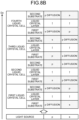
- step S206 to step S211 is executed for the M illumination devices 1_m selected as operation target devices in the multiple-device operation mode.
- the same setting change is executed for the M illumination devices 1_m selected as operation target devices in the multiple-device operation mode.
Landscapes
- Physics & Mathematics (AREA)
- Engineering & Computer Science (AREA)
- General Engineering & Computer Science (AREA)
- Chemical & Material Sciences (AREA)
- Crystallography & Structural Chemistry (AREA)
- Nonlinear Science (AREA)
- General Physics & Mathematics (AREA)
- Mathematical Physics (AREA)
- Optics & Photonics (AREA)
- Computer Networks & Wireless Communication (AREA)
- Human Computer Interaction (AREA)
- Computer Hardware Design (AREA)
- Theoretical Computer Science (AREA)
- Liquid Crystal (AREA)
- Circuit Arrangement For Electric Light Sources In General (AREA)
Applications Claiming Priority (2)
| Application Number | Priority Date | Filing Date | Title |
|---|---|---|---|
| JP2022134383 | 2022-08-25 | ||
| PCT/JP2023/023330 WO2024042837A1 (ja) | 2022-08-25 | 2023-06-23 | 照明システム及び制御装置 |
Publications (1)
| Publication Number | Publication Date |
|---|---|
| EP4580316A1 true EP4580316A1 (en) | 2025-07-02 |
Family
ID=90012852
Family Applications (1)
| Application Number | Title | Priority Date | Filing Date |
|---|---|---|---|
| EP23856954.5A Pending EP4580316A1 (en) | 2022-08-25 | 2023-06-23 | Illumination system and control device |
Country Status (7)
| Country | Link |
|---|---|
| US (1) | US20250189101A1 (https=) |
| EP (1) | EP4580316A1 (https=) |
| JP (1) | JP7746591B2 (https=) |
| KR (1) | KR102932127B1 (https=) |
| CN (1) | CN119769177A (https=) |
| MX (1) | MX2025002181A (https=) |
| WO (1) | WO2024042837A1 (https=) |
Families Citing this family (1)
| Publication number | Priority date | Publication date | Assignee | Title |
|---|---|---|---|---|
| WO2024048166A1 (ja) * | 2022-09-01 | 2024-03-07 | 株式会社ジャパンディスプレイ | 照明装置 |
Family Cites Families (4)
| Publication number | Priority date | Publication date | Assignee | Title |
|---|---|---|---|---|
| JPH0265001A (ja) | 1988-08-30 | 1990-03-05 | Sekisui Chem Co Ltd | 照明器具の調光装置 |
| JP2014093147A (ja) * | 2012-11-01 | 2014-05-19 | Japan Science & Technology Agency | 照明システムおよび照明制御方法 |
| WO2018055722A1 (ja) * | 2016-09-23 | 2018-03-29 | マクセル株式会社 | 映像投射照明装置 |
| WO2021166807A1 (ja) * | 2020-02-21 | 2021-08-26 | ソニーグループ株式会社 | 光源装置、及び画像表示装置 |
-
2023
- 2023-06-23 KR KR1020257005420A patent/KR102932127B1/ko active Active
- 2023-06-23 JP JP2024542606A patent/JP7746591B2/ja active Active
- 2023-06-23 WO PCT/JP2023/023330 patent/WO2024042837A1/ja not_active Ceased
- 2023-06-23 CN CN202380061836.XA patent/CN119769177A/zh active Pending
- 2023-06-23 EP EP23856954.5A patent/EP4580316A1/en active Pending
-
2025
- 2025-02-17 US US19/055,259 patent/US20250189101A1/en active Pending
- 2025-02-21 MX MX2025002181A patent/MX2025002181A/es unknown
Also Published As
| Publication number | Publication date |
|---|---|
| CN119769177A (zh) | 2025-04-04 |
| MX2025002181A (es) | 2025-05-02 |
| KR102932127B1 (ko) | 2026-02-27 |
| WO2024042837A1 (ja) | 2024-02-29 |
| JP7746591B2 (ja) | 2025-09-30 |
| US20250189101A1 (en) | 2025-06-12 |
| JPWO2024042837A1 (https=) | 2024-02-29 |
| KR20250040695A (ko) | 2025-03-24 |
Similar Documents
| Publication | Publication Date | Title |
|---|---|---|
| WO2023145347A1 (ja) | 照明装置及び照明制御システム | |
| US20250189101A1 (en) | Illumination system and control device | |
| US20240389209A1 (en) | Illumination device | |
| US20250311078A1 (en) | Control device for illumination device, and illumination system | |
| US20260002661A1 (en) | Control device for illumination device | |
| US12442514B2 (en) | Control device for illumination device, and illumination system | |
| US20260004750A1 (en) | Control device for illumination device | |
| US20250318034A1 (en) | Control device for illumination device | |
| US20250383068A1 (en) | Illumination system | |
| US20250327562A1 (en) | Control device for illumination device | |
| JP7615362B2 (ja) | 照明システムの制御装置 | |
| HK40118948A (zh) | 照明系统以及控制装置 | |
| US12607325B2 (en) | Control device of illumination device | |
| US20250240158A1 (en) | Communication system, illumination system, and communication method | |
| US12482435B2 (en) | Illumination device and illumination system | |
| US20240360982A1 (en) | Illumination system | |
| HK40116976A (zh) | 照明装置的控制装置以及照明系统 |
Legal Events
| Date | Code | Title | Description |
|---|---|---|---|
| STAA | Information on the status of an ep patent application or granted ep patent |
Free format text: STATUS: THE INTERNATIONAL PUBLICATION HAS BEEN MADE |
|
| PUAI | Public reference made under article 153(3) epc to a published international application that has entered the european phase |
Free format text: ORIGINAL CODE: 0009012 |
|
| STAA | Information on the status of an ep patent application or granted ep patent |
Free format text: STATUS: REQUEST FOR EXAMINATION WAS MADE |
|
| 17P | Request for examination filed |
Effective date: 20250325 |
|
| AK | Designated contracting states |
Kind code of ref document: A1 Designated state(s): AL AT BE BG CH CY CZ DE DK EE ES FI FR GB GR HR HU IE IS IT LI LT LU LV MC ME MK MT NL NO PL PT RO RS SE SI SK SM TR |
|
| DAV | Request for validation of the european patent (deleted) | ||
| DAX | Request for extension of the european patent (deleted) |