EP4580208A2 - Festkörperbildaufnahmeelement - Google Patents
Festkörperbildaufnahmeelement Download PDFInfo
- Publication number
- EP4580208A2 EP4580208A2 EP25172976.0A EP25172976A EP4580208A2 EP 4580208 A2 EP4580208 A2 EP 4580208A2 EP 25172976 A EP25172976 A EP 25172976A EP 4580208 A2 EP4580208 A2 EP 4580208A2
- Authority
- EP
- European Patent Office
- Prior art keywords
- reset
- level
- upstream
- transistor
- circuit
- Prior art date
- Legal status (The legal status is an assumption and is not a legal conclusion. Google has not performed a legal analysis and makes no representation as to the accuracy of the status listed.)
- Pending
Links
Images


Classifications
-
- H—ELECTRICITY
- H04—ELECTRIC COMMUNICATION TECHNIQUE
- H04N—PICTORIAL COMMUNICATION, e.g. TELEVISION
- H04N25/00—Circuitry of solid-state image sensors [SSIS]; Control thereof
- H04N25/70—SSIS architectures; Circuits associated therewith
- H04N25/76—Addressed sensors, e.g. MOS or CMOS sensors
- H04N25/77—Pixel circuitry, e.g. memories, A/D converters, pixel amplifiers, shared circuits or shared components
- H04N25/771—Pixel circuitry, e.g. memories, A/D converters, pixel amplifiers, shared circuits or shared components comprising storage means other than floating diffusion
-
- H—ELECTRICITY
- H04—ELECTRIC COMMUNICATION TECHNIQUE
- H04N—PICTORIAL COMMUNICATION, e.g. TELEVISION
- H04N25/00—Circuitry of solid-state image sensors [SSIS]; Control thereof
- H04N25/50—Control of the SSIS exposure
-
- H—ELECTRICITY
- H04—ELECTRIC COMMUNICATION TECHNIQUE
- H04N—PICTORIAL COMMUNICATION, e.g. TELEVISION
- H04N25/00—Circuitry of solid-state image sensors [SSIS]; Control thereof
- H04N25/60—Noise processing, e.g. detecting, correcting, reducing or removing noise
- H04N25/616—Noise processing, e.g. detecting, correcting, reducing or removing noise involving a correlated sampling function, e.g. correlated double sampling [CDS] or triple sampling
-
- H—ELECTRICITY
- H04—ELECTRIC COMMUNICATION TECHNIQUE
- H04N—PICTORIAL COMMUNICATION, e.g. TELEVISION
- H04N25/00—Circuitry of solid-state image sensors [SSIS]; Control thereof
- H04N25/60—Noise processing, e.g. detecting, correcting, reducing or removing noise
- H04N25/65—Noise processing, e.g. detecting, correcting, reducing or removing noise applied to reset noise, e.g. KTC noise related to CMOS structures by techniques other than CDS
-
- H—ELECTRICITY
- H04—ELECTRIC COMMUNICATION TECHNIQUE
- H04N—PICTORIAL COMMUNICATION, e.g. TELEVISION
- H04N25/00—Circuitry of solid-state image sensors [SSIS]; Control thereof
- H04N25/70—SSIS architectures; Circuits associated therewith
-
- H—ELECTRICITY
- H04—ELECTRIC COMMUNICATION TECHNIQUE
- H04N—PICTORIAL COMMUNICATION, e.g. TELEVISION
- H04N25/00—Circuitry of solid-state image sensors [SSIS]; Control thereof
- H04N25/70—SSIS architectures; Circuits associated therewith
- H04N25/76—Addressed sensors, e.g. MOS or CMOS sensors
- H04N25/77—Pixel circuitry, e.g. memories, A/D converters, pixel amplifiers, shared circuits or shared components
-
- H—ELECTRICITY
- H04—ELECTRIC COMMUNICATION TECHNIQUE
- H04N—PICTORIAL COMMUNICATION, e.g. TELEVISION
- H04N25/00—Circuitry of solid-state image sensors [SSIS]; Control thereof
- H04N25/70—SSIS architectures; Circuits associated therewith
- H04N25/76—Addressed sensors, e.g. MOS or CMOS sensors
- H04N25/78—Readout circuits for addressed sensors, e.g. output amplifiers or A/D converters
-
- H—ELECTRICITY
- H04—ELECTRIC COMMUNICATION TECHNIQUE
- H04N—PICTORIAL COMMUNICATION, e.g. TELEVISION
- H04N25/00—Circuitry of solid-state image sensors [SSIS]; Control thereof
- H04N25/70—SSIS architectures; Circuits associated therewith
- H04N25/79—Arrangements of circuitry being divided between different or multiple substrates, chips or circuit boards, e.g. stacked image sensors
Definitions
- the upstream circuit may further include a discharge transistor that discharges the charge from the photoelectric conversion element. This brings about an effect that the photoelectric conversion element is initialized.
- the first reset transistor may initialize the floating diffusion layer, and the discharge transistor discharges the charge from the photoelectric conversion element before a predetermined exposure start timing, and the upstream transfer transistor may transfer the charge to the floating diffusion layer at a predetermined exposure end timing. This brings about an effect that an extremely short exposure period is achieved.
- a control circuit that controls a reset power supply voltage of the upstream circuit is further provided, the first reset transistor may initialize a voltage of the floating diffusion layer to the reset power supply voltage, and the control circuit may set the reset power supply voltage to a voltage different from a voltage during an exposure period in a reading period in which the reset level and the signal level are read. This brings about an effect that photo response non-uniformity is improved.
- a difference between the reset power supply voltage in the reading period and the reset power supply voltage in the exposure period may substantially match a variation amount caused by reset feedthrough of the first reset transistor. This brings about an effect that photo response non-uniformity is improved.
- a first reset signal may be input to a gate of the first reset transistor, and an amplitude of the first reset signal may be a value obtained by adding a predetermined margin to a value corresponding to a dynamic range. This brings about an effect that a blackening phenomenon is suppressed.
- a digital signal processing section that adds a pair of consecutive frames may be further provided, and the upstream circuit may cause one of the first and second capacitive elements to hold the reset level in an exposure period of one of the pair of frames and then cause another of the first and second capacitive elements to hold the signal level, and cause the another of the first and second capacitive elements to hold the reset level in an exposure period of another of the pair of frames and then cause the one of the first and second capacitive elements to hold the signal level.
- the analog-to-digital converter may include: a comparator that compares a level of a vertical signal line that transmits the reset level and the signal level with a predetermined ramp signal and outputs a comparison result; and a counter that counts a count value over a period until the comparison result is inverted and outputs the digital signal indicating the count value.
- the comparator may include: a comparison unit that compares levels of a pair of input terminals and outputs a comparison result; and an input-side selector that selects any of the vertical signal line and a node with a predetermined reference voltage and connects the selected vertical signal line or node to one of the pair of input terminals, and the ramp signal may be input to the one of the pair of input terminals.
- the first aspect may be further provided with: a control section that determines whether or not illuminance is higher than a predetermined value on the basis of the comparison result and outputs a determination result; a correlated double sampling (CDS) processing section that performs correlated double sampling processing on the digital signal; and an output-side selector that outputs either the digital signal subjected to the correlated double sampling processing or a digital signal having a predetermined value on the basis of the determination result.
- CDS correlated double sampling
- the vertical scanning circuit may further perform control to control the plurality of rows to sequentially start the exposure. This brings about an effect that miniaturization of a pixel is facilitated.
- a second aspect of the present technology relates to a solid-state imaging element including: a photoelectric conversion section that converts incident light into a charge; a first amplification transistor that converts the charge into a voltage; a signal line that outputs a pixel signal; a first capacitive element having a first end connected to a first node which is an output destination of the first amplification transistor; a second capacitive element provided in parallel with the first capacitive element between the first amplification transistor and the signal line, the second capacitive element having a first end connected to the first node; a first selection transistor connected to the first capacitive element at a second end of the first capacitive element; a second selection transistor connected to the second capacitive element at a second end of the second capacitive element; a reset transistor of which a source or a drain is connected to a second node to which the first and second selection transistors are connected; and a second amplification transistor that has a gate connected to the second node and outputs the second
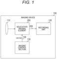
- Fig. 1 is a block diagram depicting a configuration example of an imaging device 100 in a first embodiment of the present technology.
- the imaging device 100 is a device that images image data, and includes an imaging lens 110, a solid-state imaging element 200, a recording unit 120, and an imaging control section 130.
- an imaging device 100 a digital camera or an electronic device (a smartphone, a personal computer, or the like) having an imaging function is assumed.
- the solid-state imaging element 200 images image data under the control of the imaging control section 130.
- the solid-state imaging element 200 supplies the image data to the recording unit 120 via a signal line 209.
- the vertical synchronization signal VSYNC is a signal indicating an imaging timing, and a periodic signal of a constant frequency (such as 60 hertz) is used as the vertical synchronization signal VSYNC.
- a set of the pixels 300 arrayed in the horizontal direction is referred to as a "row”
- a set of the pixels 300 arrayed in a direction perpendicular to the row is referred to as a "column”.
- the vertical scanning circuit 211 sequentially selects and drives rows and outputs analog pixel signals.
- the pixel 300 photoelectrically converts incident light to generate the analog pixel signal. This pixel 300 supplies the pixel signal to the column signal processing circuit 260 via the load MOS circuit block 250.
- the column signal processing circuit 260 executes signal processing, such as AD conversion processing and CDS processing, on the pixel signal for each column.
- the column signal processing circuit 260 supplies image data including the processed signal to the recording unit 120.
- the column signal processing circuit 260 is an example of a signal processing circuit described in the claims.
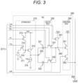
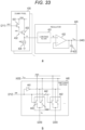
- Fig. 3 is a circuit diagram depicting a configuration example of the pixel 300 in the first embodiment of the present technology.
- the pixel 300 includes an upstream circuit 310, capacitive elements 321 and 322, a selection circuit 330, a downstream reset transistor 341, and a downstream circuit 350.
- the upstream circuit 310 includes a photoelectric conversion element 311, a transfer transistor 312, a floating diffusion (FD) reset transistor 313, an FD 314, an upstream amplification transistor 315, and a current source transistor 316.
- a photoelectric conversion element 311 a transfer transistor 312, a floating diffusion (FD) reset transistor 313, an FD 314, an upstream amplification transistor 315, and a current source transistor 316.
- FD floating diffusion
- the photoelectric conversion element 311 generates a charge by photoelectric conversion.
- the transfer transistor 312 transfers the charge from the photoelectric conversion element 311 to the FD 314 in accordance with a transfer signal trg from the vertical scanning circuit 211.
- the FD reset transistor 313 extracts and initializes the charge from the FD 314 in accordance with an FD reset signal rst from the vertical scanning circuit 211.
- the FD 314 accumulates the charge and generates a voltage corresponding to a charge amount.
- the upstream amplification transistor 315 amplifies a level of the voltage of the FD 314 and outputs the amplified voltage to an upstream node 320.
- the FD reset transistor 313 is an example of a first reset transistor described in the claims.
- the upstream amplification transistor 315 is an example of a first amplification transistor described in the claims.
- sources of the FD reset transistor 313 and the upstream amplification transistor 315 are connected to a power supply voltage VDD.
- the current source transistor 316 is connected to a drain of the upstream amplification transistor 315.
- the current source transistor 316 supplies a current id1 under the control of the vertical scanning circuit 211.
- the capacitive elements 321 and 322 have one ends connected in common to the upstream node 320 and the other ends connected to the selection circuit 330.
- the capacitive elements 321 and 322 are examples of first and second capacitive elements described in the claims.
- the selection circuit 330 includes a selection transistor 331 and a selection transistor 332.
- the selection transistor 331 opens and closes a path between the capacitive element 321 and a downstream node 340 in accordance with a selection signal ⁇ r from the vertical scanning circuit 211.
- the selection transistor 332 opens and closes a path between the capacitive element 322 and the downstream node 340 in accordance with a selection signal ⁇ s from the vertical scanning circuit 211.
- the vertical scanning circuit 211 supplies the high-level transfer signal trg over a pulse period while setting the downstream reset signal rstb and the selection signal ⁇ s to the high level for all the pixels. Therefore, a signal charge corresponding to an exposure amount is transferred to the FD 314, and a level corresponding to the level of the FD 314 at that time is held in the capacitive element 322.
- Such exposure control in which the exposure is started and ended simultaneously for all the pixels is called a global shutter system.
- This exposure control causes the upstream circuits 310 of all the pixels sequentially generate the reset level and the signal level.
- the reset level is held in the capacitive element 321, and the signal level is held in the capacitive element 322.
- the vertical scanning circuit 211 sequentially selects a row and sequentially outputs the reset level and the signal level of the row.
- the vertical scanning circuit 211 supplies the high-level selection signal ⁇ r over a predetermined period while setting the FD reset signal rst and the downstream selection signal selb of the selected row to the high level. Therefore, the capacitive element 321 is connected to the downstream node 340 so that the reset level is read.
- the selection circuit 330 of the selected row sequentially performs control to connect the capacitive element 321 to the downstream node 340, control to disconnect the capacitive elements 321 and 322 from the downstream node 340, and control to connect the capacitive element 322 to the downstream node 340. Furthermore, when the capacitive elements 321 and 322 are disconnected from the downstream node 340, the downstream reset transistor 341 of the selected row initializes the level of the downstream node 340. Furthermore, the downstream circuit 350 of the selected row sequentially reads the reset level and the signal level from the capacitive elements 321 and 322 via the downstream node 340, and outputs the reset level and the signal level to the vertical signal line 309.
- Fig. 4 is a block diagram depicting a configuration example of the load MOS circuit block 250 and the column signal processing circuit 260 in the first embodiment of the present technology.
- the column signal processing circuit 260 a plurality of ADCs 261 and a digital signal processing section 262 are arranged.
- the ADC 261 is arranged for every column. When the number of columns is I, I ADCs 261 are arranged.
- the ADC 261 converts an analog pixel signal from a corresponding column into a digital signal using a ramp signal Rmp from the DAC 213.
- the ADC 261 supplies the digital signal to the digital signal processing section 262.
- a single-slope ADC including a comparator and a counter is arranged as the ADC 261.
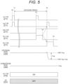
- Fig. 5 is a timing chart depicting an example of a global shutter operation in the first embodiment of the present technology.
- the vertical scanning circuit 211 supplies the high-level FD reset signals rst and transfer signal trg to all the rows (in other words, all the pixels) from a timing T0 immediately before the exposure start to a timing T1 after a lapse of a pulse period. Therefore, all the pixels are subjected to the PD reset, and the exposure is simultaneously started in all the rows.
- rst_[n] and trg_[n] in the drawing indicate signals with respect to pixels in the n-th row among N rows.
- N is an integer indicating the total number of rows, and n is an integer from one to N.
- the vertical scanning circuit 211 supplies the high-level FD reset signal rst over a pulse period while setting the downstream reset signal rstb and the selection signal ⁇ r to the high level in all the pixels at a timing T2 immediately before the end of an exposure period. Therefore, all the pixels are subjected to the FD reset, and the reset level is sampled and held.
- rstb_[n] and ⁇ r_[n] in the drawing indicate signals with respect to pixels in the n-th row.
- the vertical scanning circuit 211 returns the selection signal ⁇ r to a low level.
- the vertical scanning circuit 211 supplies the high-level transfer signal trg over a pulse period while setting the downstream reset signal rstb and the selection signal ⁇ s to the high level in all the pixels. Therefore, the signal level is sampled and held. Furthermore, a level of the upstream node 320 decreases from the reset level (VDD - Vsig) to the signal level (VDD - Vgs - Vsig).
- VDD represents the power supply voltage
- Vsig represents a net signal level obtained by CDS processing.
- Vgs represents a gate-source voltage of the upstream amplification transistor 315.
- ⁇ s_[n] in the drawing indicates a signal with respect to the pixel in the n-th row.
- the vertical scanning circuit 211 returns the selection signal ⁇ s to the low level.
- the vertical scanning circuit 211 controls the current source transistors 316 of all the rows (all the pixels) to supply the current id1.
- id1_[n] in the drawing indicates the current of the pixel in the n-th row.
- the current id1 needs to be on the order of several nanoamperes (nA) to several tens of nanoamperes (nA).
- the load MOS transistors 251 of all the columns are in the OFF state, and the current id2 is not supplied to the vertical signal line 309.
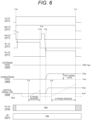
- Fig. 6 is a timing chart depicting an example of a reading operation in the first embodiment of the present technology.
- the vertical scanning circuit 211 sets the FD reset signal rst and the downstream selection signal selb of the n-th row to the high level in the reading period of the n-th row from a timing T10 to a timing T17. Furthermore, the downstream reset signals rstb of all the rows are controlled to the low level in the reading period.
- selb_[n] in the drawing indicates a signal with respect to the pixels in the n-th row.
- the vertical scanning circuit 211 supplies the high-level selection signal ⁇ r to the n-th row over a period from a timing T11 immediately after the timing T10 to a timing T13.
- the potential of the downstream node 340 becomes the reset level Vrst.
- the DAC 213 gradually increases a ramp signal Rmp over a period from the timing T12 to the timing T13 after the timing T11.
- the ADC 261 compares the ramp signal Rmp with a level Vrst' of the vertical signal line 309, and counts a count value until a comparison result is inverted. Therefore, a P-phase level (reset level) is read.
- the vertical scanning circuit 211 supplies a high-level downstream reset signal rstb to the n-th row over a pulse period from the timing T14 immediately after the timing T13. Therefore, when a parasitic capacitance exists in the downstream node 340, a history of a previous signal held in the parasitic capacitance can be erased.
- the vertical scanning circuit 211 supplies the high-level selection signal ⁇ s to the n-th row over a period from a timing T15 immediately after the initialization of the downstream node 340 to a timing T17.
- the potential of the downstream node 340 becomes the signal level Vsig.
- the signal level is lower than the reset level at the time of exposure, the signal level is higher than the reset level at the time of reading since the downstream node 340 is used as a reference.
- a difference between the reset level Vrst and the signal level Vsig corresponds to a net signal level from which reset noise and offset noise of the FD have been removed.
- the DAC 213 gradually increases a ramp signal Rmp over a period from the timing T16 to the timing T17 after the timing T15.
- the ADC 261 compares the ramp signal Rmp with a level Vrst' of the vertical signal line 309, and counts a count value until a comparison result is inverted. Therefore, a D-phase level (signal level) is read.
- the vertical scanning circuit 211 controls the current source transistor 316 of the n-th row to be read over a period from the timing T10 to the timing T17 to supply the current id1. Furthermore, the timing control circuit 212 controls the load MOS transistors 251 of all columns to supply the current id2 in a reading period of all the rows.
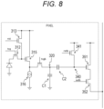
- Fig. 8 is a circuit diagram depicting a configuration example of a pixel in a comparative example.
- no selection circuit 330 is provided, and a transfer transistor is inserted between an upstream node 320 and an upstream circuit.
- capacitors C1 and C2 are inserted instead of the capacitive elements 321 and 322.
- the capacitor C1 is inserted between the upstream node 320 and a ground terminal, and the capacitor C2 is inserted between the upstream node 320 and a downstream node 340.
- Exposure control and reading control of the pixel in this comparative example are described in Figure 5.5.2 of Non-Patent Document 1, for example.
- a capacitance value of each of the capacitors C1 and C2 is C in this comparative example
- a level Vn of kTC noise at the time of exposure and reading is expressed by the following formula.
- Vn 3 ⁇ kT / C 1 / 2
- k is a Boltzmann constant
- the unit is, for example, Joule per Kelvin (J/K).
- T is an absolute temperature
- the unit is, for example, Kelvin (K).
- the unit of Vn is, for example, volt (V)
- the unit of C is, for example, farad (F).
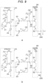
- Fig. 9 is a diagram depicting examples of states of the pixel at the time of reading the reset level and at the time of initializing the downstream node in the first embodiment of the present technology.
- a indicates the state of the pixel 300 at the time of reading the reset level
- b in the drawing indicates the state of the pixel 300 at the time of initializing the downstream node 340.
- the selection transistor 331, the selection transistor 332, and the downstream reset transistor 341 are represented by graphical symbols of switches for convenience of the description.
- the vertical scanning circuit 211 sets the selection transistor 331 in a closed state and sets the selection transistor 332 and the downstream reset transistor 341 in the open state. Therefore, the reset level is read via the downstream circuit 350.
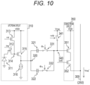
- Fig. 10 is a diagram depicting an example of a state of the pixel 300 at the time of reading the signal level in the first embodiment of the present technology.
- the downstream reset transistor 341 is driven at the time of reading as illustrated in Figs. 9 and 10 , and thus, the kTC noise occurs at that time.
- the capacitive elements 321 and 322 are disconnected at the time of driving the downstream reset transistor 341, and the parasitic capacitance Cp at that time is small. Therefore, the kTC noise at the time of reading can be ignored as compared with the kTC noise at the time of exposure. Therefore, the kTC noise at the time of exposure and reading is expressed by Formula 2.
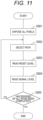
- Fig. 11 is a flowchart depicting an example of an operation of the solid-state imaging element 200 in the first embodiment of the present technology. This operation is started, for example, when a predetermined application for imaging image data is executed.
- the vertical scanning circuit 211 exposes all the pixels (step S901). Then, the vertical scanning circuit 211 selects a row to be read (step S902). The column signal processing circuit 260 reads the reset level of the row (step S903), and then reads the signal level (step S904).
- the solid-state imaging element 200 determines whether or not reading of all rows has been completed (step S905). In a case where the reading of all the rows has not been completed (Step S905: No), the solid-state imaging element 200 repeats Step S902 and the subsequent steps. On the other hand, in a case where the reading of all the rows has been completed (step S905: Yes), the solid-state imaging element 200 executes CDS processing or the like, and ends the operation for imaging. In a case where a plurality of pieces of image data is continuously imaged, steps S901 to S905 are repeatedly executed in synchronization with the vertical synchronization signal.
- the downstream reset transistor 341 initializes the downstream node 340 when the selection circuit 330 disconnects the capacitive elements 321 and 322 from the downstream node 340 in the first embodiment of the present technology. Since the capacitive elements 321 and 322 are disconnected, a level of reset noise caused by driving thereof becomes a level corresponding to a parasitic capacitance smaller than capacitances thereof. This noise reduction can improve the image quality of image data.
- the upstream reset transistor 323 initializes a level of the upstream node 320 with a power supply voltage VDD2.
- the power supply voltage VDD2 is desirably set to a value satisfying the following formula.
- VDD 2 VDD 1 ⁇ Vgs
- Vgs represents a gate-source voltage of the upstream amplification transistor 315.
- the upstream selection transistor 324 opens and closes a path between the upstream circuit 310 and the upstream node 320 in accordance with an upstream selection signal sel from the vertical scanning circuit 211.
- Fig. 13 is a timing chart depicting an example of a global shutter operation in the first modification of the first embodiment of the present technology.
- the timing chart of the first modification of the first embodiment is different from that of the first embodiment in that the vertical scanning circuit 211 further supplies an upstream reset signal rsta and an upstream selection signal sel.
- rsta_[n] and sel_[n] indicate signals with respect to pixels of the n-th row.
- the vertical scanning circuit 211 supplies the high-level upstream selection signal sel to all the pixels from a timing T2 immediately before the end of exposure to a timing T5.
- the upstream reset signal rsta is controlled to a low level.
- Fig. 14 is a timing chart depicting an example of a reading operation in the first modification of the first embodiment of the present technology.
- the upstream selection signal sel is controlled to the low level. This control causes the upstream selection transistor 324 to transition to an open state, and the upstream node 320 is disconnected from the upstream circuit 310. Therefore, it is possible to block noise from the upstream node 320 at the time of reading.
- the upstream selection transistor 324 transitions to the open state at the time of reading, and the upstream circuit 310 is disconnected from the upstream node 320, so that noise from the upstream circuit 310 can be blocked according to the first modification of the first embodiment of the present technology.
- the column signal processing circuit 260, the vertical scanning circuit 211, the timing control circuit 212, the DAC 213, and the load MOS circuit block 250 are arranged on the circuit chip 203. Circuits other than the column signal processing circuit 260 are not illustrated in the drawing.
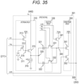
- Fig. 20 is a circuit diagram depicting a configuration example of the pixel 300 in the third embodiment of the present technology.
- the pixel 300 of the third embodiment is different from that of the first embodiment in that the power supply of the FD reset transistor 313 is disconnected from the power supply voltage VDD of the pixel 300.
- a potential of the FD 314 decreases due to reset feedthrough of the FD reset transistor 313 at a timing T0 immediately before exposure starts as illustrated in Fig. 21 .
- Such a variation amount is Vft.
- the potential of the FD 314 varies from VDD to VDD - Vft at the timing T0. Furthermore, a potential of the upstream node 320 at the time of exposure is VDD - Vft - Vsig.
- the FD reset transistor 313 transitions to an on state at the time of reading, and the FD 314 is fixed to the power supply voltage VDD in the first embodiment as illustrated in Fig. 22 .
- the variation amount Vft of the FD 314 causes the potentials of the upstream node 320 and the downstream node 340 at the time of reading to be shifted higher by about Vft.
- an amount of voltage to be shifted varies every pixel due to variations in capacitance values of the capacitive elements 321 and 322 or the parasitic capacitance, which causes the deterioration of the PRNU.
- a shift amount of the upstream node 320 in a case where the downstream node 340 is shifted by Vft is expressed by, for example, the following formula.
- Cs is a capacitance value of the capacitive element 322 on the signal level side
- ⁇ Cs is a variation in Cs
- Cp is a capacitance value of the parasitic capacitance of the downstream node 340.
- Formula 4 can be approximated by the following formula. 1 ⁇ ⁇ Cs / Cs ⁇ Cp / Cs ⁇ Vft
- the PRNU is 400 ⁇ Vrms, which is a relatively large value, according to Formula 6.
- Fig. 23 is a timing chart depicting an example of voltage control in the third embodiment of the present technology.
- the timing control circuit 212 controls the reset power supply voltage VRST to a value different from that in an exposure period.
- the timing control circuit 212 sets the reset power supply voltage VRST to the same value as the power supply voltage VDD.
- the timing control circuit 212 decreases the reset power supply voltage VRST to VDD - Vft. That is, in the reading period, the timing control circuit 212 decreases the reset power supply voltage VRST by an amount substantially matching the variation amount Vft caused by reset feedthrough. This control enables the reset level of the FD 314 to be equalized between the time of exposure and the time of reading.
- the control of the reset power supply voltage VRST enables reduction in the voltage variation amount between the FD 314 and the upstream node 320 as illustrated in the drawing. Therefore, it is possible to suppress the deterioration of the PRNU due to the variations in the capacitive elements 321 and 322 or the parasitic capacitance.
- the first to third modifications of the first embodiment and the second embodiment can also be applied to the third embodiment.
- the timing control circuit 212 decreases the reset power supply voltage VRST by the variation amount Vft caused by the reset feedthrough at the time of reading according to the third embodiment of the present technology, it is possible to equalize the reset level between the exposure and reading. Therefore, the deterioration of the photo response non-uniformity (PRNU) can be suppressed.
- PRNU photo response non-uniformity
- the solid-state imaging element 200 of a fourth embodiment is different from that of the first embodiment in that the PRNU is improved by switching a level held in the capacitive element 321 and a level held in the capacitive element 322 for each frame.
- the solid-state imaging element 200 of the fourth embodiment continuously images a plurality of frames in synchronization with a vertical synchronization signal.
- An odd-numbered frame is referred to as an "odd frame”
- an even-numbered frame is referred to as an "even frame”.
- the odd frame and the even frame are examples of a pair of frames described in the claims.
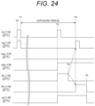
- Fig. 24 is a timing chart depicting an example of a global shutter operation of the odd frame in the fourth embodiment.
- the upstream circuit 310 in the solid-state imaging element 200 sets a selection signal ⁇ s to a high level subsequently to a selection signal ⁇ r in an exposure period of the odd frame, thereby causing the capacitive element 321 to hold the reset level, and then causing the capacitive element 322 to hold the signal level.
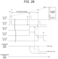
- Fig. 26 is a timing chart depicting an example of a global shutter operation of the even frame in the fourth embodiment.
- the upstream circuit 310 in the solid-state imaging element 200 sets the selection signal ⁇ r to the high level subsequently to the selection signal ⁇ s in an exposure period of the even frame, thereby causing the capacitive element 322 to hold the reset level, and then causing the capacitive element 321 to hold the signal level.
- Fig. 27 is a timing chart depicting an example of a reading operation of the even frame in the fourth embodiment of the present technology.
- the downstream circuit 350 in the solid-state imaging element 200 sets the selection signal ⁇ r to the high level subsequently to the selection signal ⁇ s to read the signal level subsequently to the reset level in the reading period of the even frame.
- the levels to be held in the capacitive elements 321 and 322 are reversed between the even frame and the odd frame. Therefore, a polarity of the PRNU is also reversed between the even frame and the odd frame.
- the column signal processing circuit 260 in the downstream stage obtains an average by adding the odd frame and the even frame. Therefore, it is possible to cancel out the PRNUs having opposite polarities.
- This control is control that is effective in imaging a moving image and adding frames. Furthermore, it is unnecessary to add an element to the pixel 300, and this control can be achieved only by changing a driving system.
- the polarity of the PRNU can be reversed between the odd frame and the even frame. Since the column signal processing circuit 260 adds the odd frame and the even frame, deterioration of the PRNU can be suppressed.
- the column signal processing circuit 260 obtains the difference between the reset level and the signal level for each column.
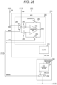
- the solid-state imaging element 200 of a fifth embodiment is different from that of the first embodiment in that whether or not the blackening phenomenon has occurred is determined for each pixel.
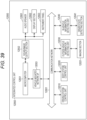
- Fig. 28 is a circuit diagram depicting a configuration example of the column signal processing circuit 260 in the fifth embodiment of the present technology.
- a plurality of ADCs 270 and a digital signal processing section 290 are arranged.
- a plurality of CDS processing sections 291 and a plurality of selectors 292 are arranged in the digital signal processing section 290.
- the ADC 270, the CDS processing section 291, and the selector 292 are provided for each column.
- the ADC 270 includes a comparator 280 and a counter 271.
- the comparator 280 compares a level of the vertical signal line 309 with a ramp signal Rmp from the DAC 213, and outputs a comparison result VCO.
- the comparison result VCO is supplied to the counter 271 and the timing control circuit 212.
- the comparator 280 includes a selector 281, capacitive elements 282 and 283, auto-zero switches 284 and 286, and a comparison unit 285.
- the selector 281 connects any of the vertical signal line 309 of a corresponding column and a node with a predetermined reference voltage VREF to a non-inverting input terminal (+) of the comparison unit 285 via the capacitive element 282 according to an input-side selection signal selin.
- the input-side selection signal selin is supplied from the timing control circuit 212.
- the selector 281 is an example of an input-side selector described in the claims.
- the comparison unit 285 compares the respective levels of the non-inverting input terminal (+) and an inverting input terminal (-), and outputs the comparison result VCO to the counter 271.
- the ramp signal Rmp is input to the inverting input terminal (-) via the capacitive element 283.
- the auto-zero switch 284 short-circuits the non-inverting input terminal (+) and an output terminal of the comparison result VCO in accordance with an auto-zero signal Az from the timing control circuit 212.
- the auto-zero switch 286 short-circuits the inverting input terminal (-) and the output terminal of the comparison result VCO in accordance with the auto-zero signal Az.
- the counter 271 counts a count value until the comparison result VCO is inverted, and outputs a digital signal CNT_out indicating the count value to the CDS processing section 291.
- the CDS processing section 291 performs CDS processing on the digital signal CNT_out.
- the CDS processing section 291 calculates a difference between the digital signal CNT_out corresponding to a reset level and the digital signal CNT_out corresponding to a signal level, and outputs the difference to the selector 292 as CDS_out.
- the microcomputer 12051 can output a control command to the body system control unit 12020 on the basis of the information regarding the outside of the vehicle which information is obtained by the outside-vehicle information detecting unit 12030.
- the microcomputer 12051 can perform cooperative control intended to prevent a glare by controlling the headlamp so as to change from a high beam to a low beam, for example, in accordance with the position of a preceding vehicle or an oncoming vehicle detected by the outside-vehicle information detecting unit 12030.
- Fig. 40 is a diagram depicting an example of the installation position of the imaging section 12031.
- the imaging section 12031 includes imaging sections 12101, 12102, 12103, 12104, and 12105.
- the imaging sections 12101, 12102, 12103, 12104, and 12105 are, for example, disposed at positions on a front nose, sideview mirrors, a rear bumper, and a back door of the vehicle 12100 as well as a position on an upper portion of a windshield within the interior of the vehicle.
- the imaging section 12101 provided to the front nose and the imaging section 12105 provided to the upper portion of the windshield within the interior of the vehicle obtain mainly an image of the front of the vehicle 12100.
- the imaging sections 12102 and 12103 provided to the sideview mirrors obtain mainly an image of the sides of the vehicle 12100.
- the imaging section 12104 provided to the rear bumper or the back door obtains mainly an image of the rear of the vehicle 12100.
- the imaging section 12105 provided to the upper portion of the windshield within the interior of the vehicle is used mainly to detect a preceding vehicle, a pedestrian, an obstacle, a signal, a traffic sign, a lane, or the like.
- Fig. 40 depicts an example of imaging ranges of the imaging sections 12101 to 12104.
- An imaging range 12111 represents the imaging range of the imaging section 12101 provided to the front nose.
- Imaging ranges 12112 and 12113 respectively represent the imaging ranges of the imaging sections 12102 and 12103 provided to the sideview mirrors.
- An imaging range 12114 represents the imaging range of the imaging section 12104 provided to the rear bumper or the back door.
- a bird's-eye image of the vehicle 12100 as viewed from above is obtained by superimposing image data imaged by the imaging sections 12101 to 12104, for example.
- At least one of the imaging sections 12101 to 12104 may have a function of obtaining distance information.
- at least one of the imaging sections 12101 to 12104 may be a stereo camera constituted of a plurality of imaging elements, or may be an imaging element having pixels for phase difference detection.
- the microcomputer 12051 can classify three-dimensional object data on three-dimensional objects into three-dimensional object data of a two-wheeled vehicle, a standard-sized vehicle, a large-sized vehicle, a pedestrian, a utility pole, and other three-dimensional objects on the basis of the distance information obtained from the imaging sections 12101 to 12104, extract the classified three-dimensional object data, and use the extracted three-dimensional object data for automatic avoidance of an obstacle.
- the microcomputer 12051 identifies obstacles around the vehicle 12100 as obstacles that the driver of the vehicle 12100 can recognize visually and obstacles that are difficult for the driver of the vehicle 12100 to recognize visually. Then, the microcomputer 12051 determines a collision risk indicating a risk of collision with each obstacle.
- the sound/image output section 12052 controls the display section 12062 so that a square contour line for emphasis is displayed so as to be superimposed on the recognized pedestrian.
- the sound/image output section 12052 may also control the display section 12062 so that an icon or the like representing the pedestrian is displayed at a desired position.
- the present technology can also have the following configurations.
Landscapes
- Engineering & Computer Science (AREA)
- Multimedia (AREA)
- Signal Processing (AREA)
- Transforming Light Signals Into Electric Signals (AREA)
- Solid State Image Pick-Up Elements (AREA)
Applications Claiming Priority (4)
| Application Number | Priority Date | Filing Date | Title |
|---|---|---|---|
| JP2020075184 | 2020-04-21 | ||
| JP2020193108 | 2020-11-20 | ||
| EP21793493.4A EP4142281B1 (de) | 2020-04-21 | 2021-02-24 | Festkörperbildaufnahmeelement |
| PCT/JP2021/006785 WO2021215105A1 (ja) | 2020-04-21 | 2021-02-24 | 固体撮像素子 |
Related Parent Applications (1)
| Application Number | Title | Priority Date | Filing Date |
|---|---|---|---|
| EP21793493.4A Division EP4142281B1 (de) | 2020-04-21 | 2021-02-24 | Festkörperbildaufnahmeelement |
Publications (2)
| Publication Number | Publication Date |
|---|---|
| EP4580208A2 true EP4580208A2 (de) | 2025-07-02 |
| EP4580208A3 EP4580208A3 (de) | 2025-08-20 |
Family
ID=78270585
Family Applications (2)
| Application Number | Title | Priority Date | Filing Date |
|---|---|---|---|
| EP25172976.0A Pending EP4580208A3 (de) | 2020-04-21 | 2021-02-24 | Festkörperbildaufnahmeelement |
| EP21793493.4A Active EP4142281B1 (de) | 2020-04-21 | 2021-02-24 | Festkörperbildaufnahmeelement |
Family Applications After (1)
| Application Number | Title | Priority Date | Filing Date |
|---|---|---|---|
| EP21793493.4A Active EP4142281B1 (de) | 2020-04-21 | 2021-02-24 | Festkörperbildaufnahmeelement |
Country Status (7)
| Country | Link |
|---|---|
| US (2) | US12047701B2 (de) |
| EP (2) | EP4580208A3 (de) |
| JP (1) | JP7668266B2 (de) |
| KR (2) | KR20230005146A (de) |
| CN (2) | CN115398885B (de) |
| DE (1) | DE112021002443T5 (de) |
| WO (1) | WO2021215105A1 (de) |
Families Citing this family (13)
| Publication number | Priority date | Publication date | Assignee | Title |
|---|---|---|---|---|
| CN117678239A (zh) * | 2021-07-26 | 2024-03-08 | 索尼半导体解决方案公司 | 固态摄像元件 |
| CN117917093A (zh) * | 2021-10-15 | 2024-04-19 | 索尼半导体解决方案公司 | 固态成像元件、成像装置和固态成像元件的控制方法 |
| EP4432688A4 (de) | 2021-11-12 | 2025-10-01 | Sony Group Corp | Festkörperbildgebungsvorrichtung, verfahren zur ansteuerung davon und elektronische vorrichtung |
| JPWO2023157489A1 (de) * | 2022-02-21 | 2023-08-24 | ||
| US20250175722A1 (en) * | 2022-03-04 | 2025-05-29 | Sony Semiconductor Solutions Corporation | Solid-state imaging element, imaging device, and method for controlling solid-state imaging element |
| WO2024004377A1 (ja) * | 2022-06-29 | 2024-01-04 | ソニーセミコンダクタソリューションズ株式会社 | 固体撮像素子、撮像装置、および、固体撮像素子の制御方法 |
| CN119487863A (zh) * | 2022-07-25 | 2025-02-18 | 索尼半导体解决方案公司 | 固态成像元件和电子设备 |
| WO2024095630A1 (ja) * | 2022-10-31 | 2024-05-10 | ソニーセミコンダクタソリューションズ株式会社 | 撮像装置 |
| TW202441976A (zh) | 2023-03-24 | 2024-10-16 | 日商索尼半導體解決方案公司 | 光檢測裝置及電子機器 |
| TW202441975A (zh) | 2023-03-24 | 2024-10-16 | 日商索尼半導體解決方案公司 | 光檢測裝置及電子機器 |
| TW202441974A (zh) | 2023-03-24 | 2024-10-16 | 日商索尼半導體解決方案公司 | 光檢測裝置及電子機器 |
| JP2025162299A (ja) | 2024-04-15 | 2025-10-27 | キヤノン株式会社 | 光電変換装置 |
| JP2025183549A (ja) | 2024-06-05 | 2025-12-17 | キヤノン株式会社 | 光電変換装置、機器 |
Family Cites Families (23)
| Publication number | Priority date | Publication date | Assignee | Title |
|---|---|---|---|---|
| JP3907559B2 (ja) * | 2002-09-04 | 2007-04-18 | リコーエレメックス株式会社 | Xdsl用通信アダプタ、回線網制御装置の屋外配線方法、遠隔監視システム、及びガス保安検針用システム |
| JP2004186790A (ja) * | 2002-11-29 | 2004-07-02 | Sony Corp | 固体撮像装置及びその駆動方法 |
| JP3951994B2 (ja) * | 2003-09-16 | 2007-08-01 | ソニー株式会社 | 固体撮像装置およびカメラシステム |
| JP5167677B2 (ja) | 2007-04-12 | 2013-03-21 | ソニー株式会社 | 固体撮像装置、固体撮像装置の駆動方法、固体撮像装置の信号処理方法および撮像装置 |
| US20090091648A1 (en) * | 2007-10-09 | 2009-04-09 | Shengmin Lin | Multi-resolution Image Sensor Array with High Image Quality Pixel Readout Circuitry |
| JP5347341B2 (ja) * | 2008-06-06 | 2013-11-20 | ソニー株式会社 | 固体撮像装置、撮像装置、電子機器、ad変換装置、ad変換方法 |
| JP5359315B2 (ja) * | 2009-01-28 | 2013-12-04 | ソニー株式会社 | 固体撮像装置、固体撮像装置の駆動方法および撮像装置 |
| JP5369779B2 (ja) * | 2009-03-12 | 2013-12-18 | ソニー株式会社 | 固体撮像装置、固体撮像装置の駆動方法および電子機器 |
| US20100271517A1 (en) * | 2009-04-24 | 2010-10-28 | Yannick De Wit | In-pixel correlated double sampling pixel |
| WO2011155442A1 (ja) * | 2010-06-11 | 2011-12-15 | 株式会社ブルックマンテクノロジ | 増幅型固体撮像装置 |
| JP5299496B2 (ja) * | 2011-11-24 | 2013-09-25 | ソニー株式会社 | 固体撮像素子及びカメラ装置 |
| TWI530183B (zh) | 2011-12-08 | 2016-04-11 | 新力股份有限公司 | An imaging element, a control method, and an imaging device |
| JP2014096669A (ja) * | 2012-11-08 | 2014-05-22 | Canon Inc | 光電変換装置の駆動方法、光電変換装置、光電変換システム |
| JP2014112760A (ja) * | 2012-12-05 | 2014-06-19 | Sony Corp | 固体撮像装置および電子機器 |
| US9843757B2 (en) | 2015-06-24 | 2017-12-12 | Stmicroelectronics (Research & Development) Limited | Optical electronic device including enhanced global shutter pixel array and related methods |
| US9654712B2 (en) | 2015-10-07 | 2017-05-16 | Semiconductor Components Industries, Llc | Pixels with a global shutter and high dynamic range |
| US10771719B2 (en) * | 2016-07-28 | 2020-09-08 | Sony Semiconductor Solutions Corporation | Imaging element |
| US10021334B2 (en) | 2016-08-29 | 2018-07-10 | Stmicroelectronics (Research & Development) Limited | Pixel circuit and method of operating the same |
| TWI754696B (zh) * | 2016-12-14 | 2022-02-11 | 日商索尼半導體解決方案公司 | 固體攝像元件及電子機器 |
| US10070090B2 (en) * | 2017-02-03 | 2018-09-04 | SmartSens Technology (U.S.), Inc. | Stacked image sensor pixel cell with selectable shutter modes and in-pixel CDS |
| JP2018186478A (ja) * | 2017-04-25 | 2018-11-22 | ソニーセミコンダクタソリューションズ株式会社 | 固体撮像素子、撮像装置、および、固体撮像素子の制御方法 |
| EP3624441B1 (de) * | 2017-05-10 | 2024-12-25 | Brillnics Singapore Pte. Ltd. | Festkörperbildaufnahmevorrichtung, ansteuerverfahren für festkörperbildaufnahmevorrichtung und elektronische vorrichtung |
| US20200244900A1 (en) * | 2019-01-28 | 2020-07-30 | Semiconductor Components Industries, Llc | Backside illuminated image sensors with pixels that have high dynamic range, dynamic charge overflow, and global shutter scanning |
-
2021
- 2021-02-24 EP EP25172976.0A patent/EP4580208A3/de active Pending
- 2021-02-24 EP EP21793493.4A patent/EP4142281B1/de active Active
- 2021-02-24 KR KR1020227035272A patent/KR20230005146A/ko active Pending
- 2021-02-24 WO PCT/JP2021/006785 patent/WO2021215105A1/ja not_active Ceased
- 2021-02-24 CN CN202180028744.2A patent/CN115398885B/zh active Active
- 2021-02-24 CN CN202411670371.0A patent/CN119629501A/zh active Pending
- 2021-02-24 DE DE112021002443.4T patent/DE112021002443T5/de active Pending
- 2021-02-24 KR KR1020247040465A patent/KR20250004111A/ko active Pending
- 2021-02-24 JP JP2022516866A patent/JP7668266B2/ja active Active
- 2021-02-24 US US17/995,745 patent/US12047701B2/en active Active
-
2024
- 2024-06-18 US US18/746,479 patent/US12581218B2/en active Active
Non-Patent Citations (1)
| Title |
|---|
| JAE-KYU LEE: " A 2.1e-Temporal Noise and -105 dB Parasitic Light Sensitivity Backside-Illuminated 2.3 µm-Pixe Voltage-Domain Global Shutter CMOS Image Sensor Using High-Capacity DRAM Capacitor Technology", ISSCC, 2020 |
Also Published As
| Publication number | Publication date |
|---|---|
| EP4142281B1 (de) | 2025-05-21 |
| KR20230005146A (ko) | 2023-01-09 |
| JPWO2021215105A1 (de) | 2021-10-28 |
| US12047701B2 (en) | 2024-07-23 |
| EP4580208A3 (de) | 2025-08-20 |
| KR20250004111A (ko) | 2025-01-07 |
| WO2021215105A1 (ja) | 2021-10-28 |
| US20230188867A1 (en) | 2023-06-15 |
| CN115398885A (zh) | 2022-11-25 |
| US20240340551A1 (en) | 2024-10-10 |
| JP7668266B2 (ja) | 2025-04-24 |
| EP4142281A4 (de) | 2023-09-20 |
| US12581218B2 (en) | 2026-03-17 |
| DE112021002443T5 (de) | 2023-02-23 |
| CN119629501A (zh) | 2025-03-14 |
| EP4142281A1 (de) | 2023-03-01 |
| CN115398885B (zh) | 2026-03-20 |
Similar Documents
| Publication | Publication Date | Title |
|---|---|---|
| US12581218B2 (en) | Solid-state imaging element | |
| EP4142280B1 (de) | Festkörperbildaufnahmeelement und bildaufnahmevorrichtung | |
| US12457436B2 (en) | Solid-state imaging element, imaging device, and solid-state imaging element control method | |
| US20240414450A1 (en) | Solid-state imaging element | |
| US20240414451A1 (en) | Solid-state imaging element, imaging device, and method for controlling solid-state imaging element | |
| US20240373143A1 (en) | Solid-state imaging element, imaging device, and solid-state imaging element control method | |
| WO2023063024A1 (ja) | 固体撮像素子、撮像装置、および、固体撮像素子の制御方法 | |
| US20250150730A1 (en) | Solid-state imaging element, imaging device, and method for controlling solid-state imaging element | |
| US12452555B2 (en) | Solid-state imaging element | |
| US20250184632A1 (en) | Solid-state imaging element, imaging device, and method for controlling solid-state imaging element | |
| US20250159383A1 (en) | Solid-state imaging element, imaging device, and method for controlling solid-state imaging element | |
| US20250175722A1 (en) | Solid-state imaging element, imaging device, and method for controlling solid-state imaging element | |
| US20250380055A1 (en) | Solid-state imaging element, imaging device, and method of controlling solid-state imaging element |
Legal Events
| Date | Code | Title | Description |
|---|---|---|---|
| PUAI | Public reference made under article 153(3) epc to a published international application that has entered the european phase |
Free format text: ORIGINAL CODE: 0009012 |
|
| STAA | Information on the status of an ep patent application or granted ep patent |
Free format text: STATUS: REQUEST FOR EXAMINATION WAS MADE |
|
| 17P | Request for examination filed |
Effective date: 20250519 |
|
| AC | Divisional application: reference to earlier application |
Ref document number: 4142281 Country of ref document: EP Kind code of ref document: P |
|
| AK | Designated contracting states |
Kind code of ref document: A2 Designated state(s): AL AT BE BG CH CY CZ DE DK EE ES FI FR GB GR HR HU IE IS IT LI LT LU LV MC MK MT NL NO PL PT RO RS SE SI SK SM TR |
|
| REG | Reference to a national code |
Ref country code: DE Ref legal event code: R079 Free format text: PREVIOUS MAIN CLASS: H04N0025650000 Ipc: H04N0025771000 |
|
| PUAL | Search report despatched |
Free format text: ORIGINAL CODE: 0009013 |
|
| AK | Designated contracting states |
Kind code of ref document: A3 Designated state(s): AL AT BE BG CH CY CZ DE DK EE ES FI FR GB GR HR HU IE IS IT LI LT LU LV MC MK MT NL NO PL PT RO RS SE SI SK SM TR |
|
| RIC1 | Information provided on ipc code assigned before grant |
Ipc: H04N 25/771 20230101AFI20250714BHEP Ipc: H04N 25/78 20230101ALI20250714BHEP Ipc: H04N 25/79 20230101ALI20250714BHEP Ipc: H04N 25/65 20230101ALI20250714BHEP |
|
| GRAP | Despatch of communication of intention to grant a patent |
Free format text: ORIGINAL CODE: EPIDOSNIGR1 |
|
| STAA | Information on the status of an ep patent application or granted ep patent |
Free format text: STATUS: GRANT OF PATENT IS INTENDED |
|
| INTG | Intention to grant announced |
Effective date: 20260212 |