EP4580031A1 - Wechselrichter und spannungssteuerungsverfahren dafür - Google Patents
Wechselrichter und spannungssteuerungsverfahren dafür Download PDFInfo
- Publication number
- EP4580031A1 EP4580031A1 EP24222736.1A EP24222736A EP4580031A1 EP 4580031 A1 EP4580031 A1 EP 4580031A1 EP 24222736 A EP24222736 A EP 24222736A EP 4580031 A1 EP4580031 A1 EP 4580031A1
- Authority
- EP
- European Patent Office
- Prior art keywords
- bus
- balancing
- bridge arm
- voltage threshold
- inverter
- Prior art date
- Legal status (The legal status is an assumption and is not a legal conclusion. Google has not performed a legal analysis and makes no representation as to the accuracy of the status listed.)
- Pending
Links
Images


Classifications
-
- H—ELECTRICITY
- H02—GENERATION; CONVERSION OR DISTRIBUTION OF ELECTRIC POWER
- H02M—APPARATUS FOR CONVERSION BETWEEN AC AND AC, BETWEEN AC AND DC, OR BETWEEN DC AND DC, AND FOR USE WITH MAINS OR SIMILAR POWER SUPPLY SYSTEMS; CONVERSION OF DC OR AC INPUT POWER INTO SURGE OUTPUT POWER; CONTROL OR REGULATION THEREOF
- H02M7/00—Conversion of AC power input into DC power output; Conversion of DC power input into AC power output
- H02M7/42—Conversion of DC power input into AC power output without possibility of reversal
- H02M7/44—Conversion of DC power input into AC power output without possibility of reversal by static converters
- H02M7/48—Conversion of DC power input into AC power output without possibility of reversal by static converters using discharge tubes with control electrode or semiconductor devices with control electrode
- H02M7/53—Conversion of DC power input into AC power output without possibility of reversal by static converters using discharge tubes with control electrode or semiconductor devices with control electrode using devices of a triode or transistor type requiring continuous application of a control signal
- H02M7/537—Conversion of DC power input into AC power output without possibility of reversal by static converters using discharge tubes with control electrode or semiconductor devices with control electrode using devices of a triode or transistor type requiring continuous application of a control signal using semiconductor devices only, e.g. single switched pulse inverters
- H02M7/5387—Conversion of DC power input into AC power output without possibility of reversal by static converters using discharge tubes with control electrode or semiconductor devices with control electrode using devices of a triode or transistor type requiring continuous application of a control signal using semiconductor devices only, e.g. single switched pulse inverters in a bridge configuration
- H02M7/53871—Conversion of DC power input into AC power output without possibility of reversal by static converters using discharge tubes with control electrode or semiconductor devices with control electrode using devices of a triode or transistor type requiring continuous application of a control signal using semiconductor devices only, e.g. single switched pulse inverters in a bridge configuration with automatic control of output voltage or current
-
- H—ELECTRICITY
- H02—GENERATION; CONVERSION OR DISTRIBUTION OF ELECTRIC POWER
- H02J—ELECTRIC POWER NETWORKS; CIRCUIT ARRANGEMENTS OR SYSTEMS FOR SUPPLYING OR DISTRIBUTING ELECTRIC POWER; SYSTEMS FOR STORING ELECTRIC ENERGY
- H02J3/00—Circuit arrangements for AC mains or AC distribution networks
- H02J3/38—Arrangements for feeding a single network from two or more generators or sources in parallel; Arrangements for feeding already energised networks from additional generators or sources in parallel
-
- H—ELECTRICITY
- H02—GENERATION; CONVERSION OR DISTRIBUTION OF ELECTRIC POWER
- H02M—APPARATUS FOR CONVERSION BETWEEN AC AND AC, BETWEEN AC AND DC, OR BETWEEN DC AND DC, AND FOR USE WITH MAINS OR SIMILAR POWER SUPPLY SYSTEMS; CONVERSION OF DC OR AC INPUT POWER INTO SURGE OUTPUT POWER; CONTROL OR REGULATION THEREOF
- H02M7/00—Conversion of AC power input into DC power output; Conversion of DC power input into AC power output
- H02M7/42—Conversion of DC power input into AC power output without possibility of reversal
- H02M7/44—Conversion of DC power input into AC power output without possibility of reversal by static converters
- H02M7/48—Conversion of DC power input into AC power output without possibility of reversal by static converters using discharge tubes with control electrode or semiconductor devices with control electrode
- H02M7/4803—Conversion of DC power input into AC power output without possibility of reversal by static converters using discharge tubes with control electrode or semiconductor devices with control electrode with means for reducing DC component from AC output voltage
-
- H—ELECTRICITY
- H02—GENERATION; CONVERSION OR DISTRIBUTION OF ELECTRIC POWER
- H02M—APPARATUS FOR CONVERSION BETWEEN AC AND AC, BETWEEN AC AND DC, OR BETWEEN DC AND DC, AND FOR USE WITH MAINS OR SIMILAR POWER SUPPLY SYSTEMS; CONVERSION OF DC OR AC INPUT POWER INTO SURGE OUTPUT POWER; CONTROL OR REGULATION THEREOF
- H02M7/00—Conversion of AC power input into DC power output; Conversion of DC power input into AC power output
- H02M7/42—Conversion of DC power input into AC power output without possibility of reversal
- H02M7/44—Conversion of DC power input into AC power output without possibility of reversal by static converters
- H02M7/48—Conversion of DC power input into AC power output without possibility of reversal by static converters using discharge tubes with control electrode or semiconductor devices with control electrode
- H02M7/483—Converters with outputs that each can have more than two voltages levels
- H02M7/4833—Capacitor voltage balancing
-
- H—ELECTRICITY
- H02—GENERATION; CONVERSION OR DISTRIBUTION OF ELECTRIC POWER
- H02M—APPARATUS FOR CONVERSION BETWEEN AC AND AC, BETWEEN AC AND DC, OR BETWEEN DC AND DC, AND FOR USE WITH MAINS OR SIMILAR POWER SUPPLY SYSTEMS; CONVERSION OF DC OR AC INPUT POWER INTO SURGE OUTPUT POWER; CONTROL OR REGULATION THEREOF
- H02M7/00—Conversion of AC power input into DC power output; Conversion of DC power input into AC power output
- H02M7/42—Conversion of DC power input into AC power output without possibility of reversal
- H02M7/44—Conversion of DC power input into AC power output without possibility of reversal by static converters
- H02M7/48—Conversion of DC power input into AC power output without possibility of reversal by static converters using discharge tubes with control electrode or semiconductor devices with control electrode
- H02M7/53—Conversion of DC power input into AC power output without possibility of reversal by static converters using discharge tubes with control electrode or semiconductor devices with control electrode using devices of a triode or transistor type requiring continuous application of a control signal
- H02M7/537—Conversion of DC power input into AC power output without possibility of reversal by static converters using discharge tubes with control electrode or semiconductor devices with control electrode using devices of a triode or transistor type requiring continuous application of a control signal using semiconductor devices only, e.g. single switched pulse inverters
- H02M7/539—Conversion of DC power input into AC power output without possibility of reversal by static converters using discharge tubes with control electrode or semiconductor devices with control electrode using devices of a triode or transistor type requiring continuous application of a control signal using semiconductor devices only, e.g. single switched pulse inverters with automatic control of output wave form or frequency
- H02M7/5395—Conversion of DC power input into AC power output without possibility of reversal by static converters using discharge tubes with control electrode or semiconductor devices with control electrode using devices of a triode or transistor type requiring continuous application of a control signal using semiconductor devices only, e.g. single switched pulse inverters with automatic control of output wave form or frequency by pulse-width modulation
Definitions
- This application relates to the field of power electronics technologies, and in particular, to an inverter and a voltage control method thereof.
- An inverter is a converter for converting a direct current (direct current, DC) into an alternating current (alternating current, AC).
- the inverter is usually connected to a photovoltaic panel and a load, and is configured to: convert a direct current DC from the photovoltaic panel into an alternating current AC, and then transmit the alternating current AC to the load, to supply power to the load.
- the inverter usually includes two capacitors and a switching bridge arm.
- the two capacitors are connected in series between a positive bus and a negative bus (that is, positive and negative buses), and a series connection node of the two capacitors is also referred to as a bus midpoint.
- the switching bridge arm is connected to the positive bus and the negative bus, the switching bridge arm has a plurality of outputs, and each output and the bus midpoint form one pair of output ports.
- the inverter is connected to the load through a plurality of pairs of output ports.
- This application provides an inverter and a voltage control method thereof, to resolve a technical problem of voltage imbalance between positive and negative buses in a related technology.
- the switching bridge arm is connected to the positive bus and the negative bus, the switching bridge arm has a plurality of outputs, and each of the plurality of outputs and the bus midpoint form one pair of output ports.
- the control circuit is configured to: obtain a direct current voltage (direct current voltage, DCV) component of a target output port in the plurality of pairs of output ports, and a bus voltage difference between the positive bus and the negative bus; and when the bus voltage difference is greater than or equal to a first voltage threshold and less than or equal to a second voltage threshold, output a first balancing modulation signal to the balancing bridge arm, where the first balancing modulation signal is used to control the balancing bridge arm to adjust a current flowing through the first inductor, to reduce the DCV component of the target output port to a target range.
- DCV direct current voltage
- the control circuit may control the balancing bridge arm to adjust the DCV component of the target output port.
- the target output port is connected to the bus midpoint. Therefore, the control circuit controls the balancing bridge arm to adjust the DCV component of the target output port, so that a voltage of the bus midpoint can be adjusted.
- the DCV component of the target output port is reduced to the target range, so that the bus voltage difference can be less than the first voltage threshold. In other words, the bus voltage difference canbe reduced, so that voltages on positive and negative buses are balanced.
- control circuit may be further configured to: when the bus voltage difference is greater than or equal to a third voltage threshold, output a second balancing modulation signal to the balancing bridge arm, where the second balancing modulation signal is used to control the balancing bridge arm to adjust the current flowing through the first inductor, to reduce the bus voltage difference, where the third voltage threshold is greater than the second voltage threshold.
- the control circuit can further output the second balancing modulation signal to the balancing bridge arm, to directly reduce the bus voltage difference, so that the voltages on the positive and negative buses are balanced. Then, if the bus voltage difference is still greater than or equal to the first voltage threshold and less than or equal to the second voltage threshold, the control circuit can further control the balancing bridge arm to adjust the DCV component of the target output port, to further reduce the bus voltage difference, so that the voltages on the positive and negative buses are more balanced. In this way, it can be ensured that precision of adjusting the bus voltage difference is better, and adjustment efficiency is high.
- control circuit may be further configured to: when the bus voltage difference increases from being less than or equal to the second voltage threshold to being greater than the second voltage threshold and less than the third voltage threshold, output the first balancing modulation signal to the balancing bridge arm; and when the bus voltage difference decreases from being greater than or equal to the third voltage threshold to being less than the third voltage threshold and greater than the second voltage threshold, output the second balancing modulation signal to the balancing bridge arm.
- the control circuit may continue to output the first balancing modulation signal to the balancing bridge arm to balance the voltages on the positive and negative buses.
- the control circuit may continue to output the second balancing modulation signal to the balancing bridge arm to balance the voltages on the positive and negative buses.
- the balancing bridge arm may include two first switching transistors.
- the two first switching transistors may be connected in series between the positive bus and the negative bus, and a series connection node of the two first switching transistors may be connected to the first inductor.
- the first balancing modulation signal may be used to control turn-on and turn-off of the two first switching transistors, to adjust a current output to the first inductor, and therefore adjust the DCV component of the target output port or the bus voltage difference to balance the voltages on the positive and negative buses.
- control circuit 03 may preset the control mode flag based on the bus voltage difference, so that when the bus voltage difference is between the second voltage threshold Y and the third voltage threshold X, the corresponding balancing modulation signal is directly output to the balancing bridge arm 01, to quickly balance the voltages on the positive and negative buses.
- control mode flag may further include an initial mode flag C.
- the control circuit 03 may be configured to adjust the initial mode flag C to the first mode flag A or the second mode flag B based on the bus voltage difference.
- control mode flag may be identified in a binary form.
- the initial mode flag C may be 00
- the first mode flag A may be 10
- the second mode flag B may be 01.
- control circuit 03 may prestore processing logic of the first mode flag A and processing logic of the second mode flag B, and the two mode flags have different processing logic.
- the control circuit 03 may correspondingly output the first balancing modulation signal to the balancing bridge arm 0 1 by executing the processing logic of the first mode flag A, and may correspondingly output the second balancing modulation signal to the balancing bridge arm 0 1 by executing the processing logic of the second mode flag B.
- the control circuit 03 may directly execute processing logic of the current control mode flag to output the corresponding balancing modulation signal to the balancing bridge arm 01.
- the control circuit 03 may output the corresponding first balancing modulation signal to the balancing bridge arm 01, to control the balancing bridge arm 01 to adjust the DCV component of the target output port. If the current control mode flag is the second mode flag B, the control circuit 03 may output the corresponding second balancing modulation signal to the balancing bridge arm 01, to control the balancing bridge arm 01 to adjust the bus voltage difference.
- the first balancing modulation signal may be a pulse width modulation (pulse width modulation, PWM) driver gating signal.
- the second balancing modulation signal may also be a PWM driver gating signal. Outputting of the first balancing modulation signal and the second balancing modulation signal by the control circuit 03 may also be referred to as sending of PWM driver gating signals.
- first balancing modulation signal and the second balancing modulation signal may be different.
- both the first balancing modulation signal and the second balancing modulation signal are PWM driver gating signals. That the first balancing modulation signal and the second balancing modulation signal are different may mean that duty cycles of the PWM driver gating signals are different, frequencies of the PWM driver gating signals are different, and/or resolutions of the PWM driver gating signals are different.
- control circuit 03 may output the corresponding balancing modulation signal to the balancing bridge arm 01 based on a value of the bus voltage difference, and also output the corresponding balancing modulation signal to the balancing bridge arm 01 based on the current control mode flag. Therefore, flexibility is better.
- control circuit 03 may be configured to perform the following steps:
- control circuit 03 may further first set (for example, adjust) the control mode flag to the second mode flag B in step A4. Then, the control circuit 03 executes the processing logic of the second mode flag B (in other words, selects the second mode flag B), to output the second balancing modulation signal to the balancing bridge arm 01.
- control mode flag may alternatively not need to be set in the control circuit 03.
- control circuit 03 may further directly output the second balancing modulation signal to the balancing bridge arm 01 based on the fact that the bus voltage difference is greater than the second voltage threshold Y and less than the third voltage threshold X. In other words, the control circuit 03 may continuously output the second balancing modulation signal to the balancing bridge arm 01 until the bus voltage difference is less than the second voltage threshold Y.
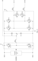
- the balancing bridge arm 01 may include two first switching transistors T11 and T12.
- the two first switching transistors T11 and T12 may be connected in series between the positive bus BUS+ and the negative bus BUS-, and a series connection node of the two first switching transistors T11 and T12 may be connected to the first inductor L1.
- the series connection node of the two first switching transistors T11 and T12 may be connected to one end of the first inductor L1, and the other end of the first inductor L1 may be connected to the bus midpoint N.
- control circuit 03 may be connected to gates of the two first switching transistors T11 and T12.
- the switching bridge arm 02 may have the two outputs U and W.
- the inverter 00 may have the pair of output ports UO formed by the output U and the bus midpoint N, and the other pair of output ports WO formed by the output W and the bus midpoint N. That is, the inverter 00 may have the two pairs of output ports UO and WO.
- the inverter 00 of this structure may be a single-phase inverter.
- the switching bridge arm 02 may include two second switching transistors T21 and T22, two third switching transistors T31 and T32, and two fourth switching transistors T41 and T42.
- the two second switching transistors T21 and T22 may be connected in series between the positive bus BUS+ and the negative bus BUS-, and a series connection node of the two second switching transistors T21 and T22 may correspond to one of the two outputs U and W, for example, the output U.
- the two third switching transistors T31 and T32 may be connected in series between the positive bus BUS+ and the negative bus BUS-, and a series connection node of the two third switching transistors T31 and T32 corresponds to the other one of the two outputs U and W, for example, the output W.
- the two fourth switching transistors T41 and T42 may be connected in series between the two outputs U and W.
- the first sampling circuit 04 may be connected to the positive bus BUS+, the negative bus BUS-, and the control circuit 03.
- the inverter 00 described in this embodiment of this application may further include a plurality of second inductors L2 that are in one-to-one correspondence with the plurality of outputs of the switching bridge arm 02.
- Each of the plurality of second inductors L2 may be connected to one corresponding output.
- the second inductors L2 and the first inductor L1 described above may be all coupling inductors, and may be all configured to filter signals.
- the inverter 00 may further include a second inductor L2 connected to the output U, and the other second inductor L2 connected to the output W. That is, the inverter 00 may include two second inductors L2.
- the coupling inductor is replaced with a discrete inductor, to directly adjust the DCV component of the target output port through the inverter-side components, so as to balance the voltages on the positive and negative buses.
- the control circuit 03 outputs the first balancing modulation signal to the balancing bridge arm 01 to adjust the DCV component of the target output port, so that use of the inductor is more flexible.
- the discrete inductor with the high costs may not need to be disposed in the inverter.
- hardware costs of the inverter can be reduced, and this facilitates mass production of the inverter.
- this embodiment of the present disclosure provides the inverter.
- the inverter has the plurality of pairs of output ports, and the inverter includes the balancing bridge arm, the switching bridge arm, the two capacitors, the first inductor, and the control circuit.
- the two capacitors are connected in series between the positive and negative buses, and each pair of output ports is connected to the series connection node (namely, the bus midpoint) of the two capacitors.
- the control circuit can obtain the DCV component of the target output port in the plurality of pairs of output ports and the bus voltage difference between the positive and negative buses; and when the bus voltage difference is greater than or equal to the first voltage threshold and less than or equal to the second voltage threshold, can output the balancing modulation signal to the balancing bridge arm, to control the balancing bridge arm to reduce the DCV component of the target output port to the target range by adjusting the current flowing through the first inductor, so that the bus voltage difference is reduced to be less than the first voltage threshold. In other words, the bus voltage difference can be reduced, so that the voltages on the positive and negative buses can be balanced.
- the inverter 00 has a plurality of pairs of output ports (for example, pairs of output ports UO and WO), and the inverter 00 includes a balancing bridge arm 01, a switching bridge arm 02, two capacitors C1 and C2, and a first inductor L1.
- the two capacitors C1 and C2 are connected in series between a positive bus BUS+ and a negative bus BUS-, a series connection node between the two capacitors C1 and C2 is a bus midpoint N, and the positive bus BUS+ and the negative bus BUS- are configured to connect to a direct current power supply device 10.
- the balancing bridge arm 01 is connected to the positive bus BUS+ and the negative bus BUS-, and is connected to the bus midpoint N through the first inductor L1.
- the switching bridge arm 02 is connected to the positive bus BUS+ and the negative bus BUS-, the switching bridge arm 02 has a plurality of outputs (for example, two outputs U and W), and each of the plurality of outputs and the bus midpoint N form one pair of output ports. Therefore, the plurality of outputs and the bus midpoint N can form the plurality of pairs of output ports.
- the method can be applied to a control circuit 03 included in the inverter 00. As shown in FIG. 5 , the method includes the following steps.
- Step 501 Obtain a direct current voltage DCV component of a target output port in the plurality of pairs of output ports of the inverter, and a bus voltage difference between the positive bus and the negative bus.
- the control circuit 03 may include a first sampling circuit 04 and a second sampling circuit 05.
- the control circuit 03 may obtain the DCV component of the target output port through the first sampling circuit 04, and may obtain the bus voltage difference through the second sampling circuit 05.
- Step 502 When the bus voltage difference is greater than or equal to a first voltage threshold and less than or equal to a second voltage threshold, output a first balancing modulation signal to the balancing bridge arm.
- the first balancing modulation signal is used to control the balancing bridge arm 01 to adjust a current flowing through the first inductor L1, to reduce the DCV component of the target output port to a target range, so that the bus voltage difference is less than the first voltage threshold, and voltages on positive and negative buses are balanced.
- FIG. 6 is a flowchart of another voltage control method for an inverter according to an embodiment of this application. As shown in FIG. 6 , the voltage control method may further include the following step.
- Step 503 When the bus voltage difference is greater than or equal to a third voltage threshold, output a second balancing modulation signal to the balancing bridge arm.
- the second balancing modulation signal may be used to control the balancing bridge arm to adjust the current flowing through the first inductor L1, to reduce the bus voltage difference.
- the bus voltage difference is reduced to be less than the third voltage threshold.
- the third voltage threshold may be greater than the second voltage threshold.
- the voltage control method may further include the following steps.
- Step 504 When the bus voltage difference increases from being less than or equal to the second voltage threshold to being greater than the second voltage threshold and less than the third voltage threshold, output the first balancing modulation signal to the balancing bridge arm.
- control circuit 03 may continue to output the first balancing modulation signal to the balancing bridge arm 01, to balance the voltages on the positive and negative buses.
- Step 505 When the bus voltage difference decreases from being greater than or equal to the third voltage threshold to being less than the third voltage threshold and greater than the second voltage threshold, output the second balancing modulation signal to the balancing bridge arm.
- control circuit 03 may continue to output the second balancing modulation signal to the balancing bridge arm 01, to balance the voltages on the positive and negative buses.
- the control circuit 03 may first perform step 503 after performing step 501, to be specific, first output the second balancing modulation signal to the balancing bridge arm 01, to control the balancing bridge arm 01 to directly reduce the bus voltage difference to be less than the third voltage threshold, in other words, first coarsely adjust the bus voltage difference to balance the voltages on the positive and negative buses.
- the control circuit 03 may further perform step 502, to be specific, further output the first balancing modulation signal to the balancing bridge arm 01, to control the balancing bridge arm 01 to reduce the DCV component of the target output port, so that the bus voltage difference can be further less than the smaller first voltage threshold Z, in other words, finely adjust the DCV component of the target output port to further balance the voltages on the positive and negative buses.
- step 503 after performing step 503, to be specific, after outputting the second balancing modulation signal to the balancing bridge arm 01, if the bus voltage difference is greater than the second voltage threshold and less than the third voltage threshold, the control circuit 03 may continue to perform step 505, to be specific, may continue to output the second balancing modulation signal to the balancing bridge arm 01.
- step 504 after outputting the first balancing modulation signal to the balancing bridge arm 01, if the bus voltage difference is greater than the second voltage threshold and less than the third voltage threshold, the control circuit 03 may continue to perform step 504, to be specific, may continue to output the first balancing modulation signal to the balancing bridge arm 01.
- step 504 and step 505 may be deleted based on a situation.
- the control circuit may further directly output the second balancing modulation signal to the balancing bridge arm based on a fact that the bus voltage difference is greater than the second voltage threshold and less than the third voltage threshold.
- step 503 may be deleted based on a situation.
- the control circuit may directly control the balancing bridge arm to adjust the DCV component of the target output port, to finely adjust the bus voltage difference to balance the voltages on the positive and negative buses.
Landscapes
- Engineering & Computer Science (AREA)
- Power Engineering (AREA)
- Inverter Devices (AREA)
Applications Claiming Priority (1)
| Application Number | Priority Date | Filing Date | Title |
|---|---|---|---|
| CN202311861805.0A CN120237971A (zh) | 2023-12-28 | 2023-12-28 | 逆变器及其电压控制方法 |
Publications (1)
| Publication Number | Publication Date |
|---|---|
| EP4580031A1 true EP4580031A1 (de) | 2025-07-02 |
Family
ID=94083297
Family Applications (1)
| Application Number | Title | Priority Date | Filing Date |
|---|---|---|---|
| EP24222736.1A Pending EP4580031A1 (de) | 2023-12-28 | 2024-12-23 | Wechselrichter und spannungssteuerungsverfahren dafür |
Country Status (2)
| Country | Link |
|---|---|
| EP (1) | EP4580031A1 (de) |
| CN (1) | CN120237971A (de) |
Citations (2)
| Publication number | Priority date | Publication date | Assignee | Title |
|---|---|---|---|---|
| CN115589169A (zh) * | 2022-12-13 | 2023-01-10 | 麦田能源有限公司 | 基于瞬时特性的逆变器的控制方法、装置及逆变器系统 |
| CN116232102A (zh) * | 2022-12-19 | 2023-06-06 | 华为数字能源技术有限公司 | 逆变器及其控制方法 |
-
2023
- 2023-12-28 CN CN202311861805.0A patent/CN120237971A/zh active Pending
-
2024
- 2024-12-23 EP EP24222736.1A patent/EP4580031A1/de active Pending
Patent Citations (3)
| Publication number | Priority date | Publication date | Assignee | Title |
|---|---|---|---|---|
| CN115589169A (zh) * | 2022-12-13 | 2023-01-10 | 麦田能源有限公司 | 基于瞬时特性的逆变器的控制方法、装置及逆变器系统 |
| CN116232102A (zh) * | 2022-12-19 | 2023-06-06 | 华为数字能源技术有限公司 | 逆变器及其控制方法 |
| EP4432545A1 (de) * | 2022-12-19 | 2024-09-18 | Huawei Digital Power Technologies Co., Ltd. | Wechselrichter und steuerungsverfahren dafür |
Non-Patent Citations (1)
| Title |
|---|
| HE GUOFENG ET AL: "A Novel Control Strategy of Suppressing DC Current Injection to the Grid for Single-Phase PV Inverter", IEEE TRANSACTIONS ON POWER ELECTRONICS, INSTITUTE OF ELECTRICAL AND ELECTRONICS ENGINEERS, USA, vol. 30, no. 3, 1 March 2015 (2015-03-01), pages 1266 - 1274, XP011561472, ISSN: 0885-8993, [retrieved on 20141014], DOI: 10.1109/TPEL.2014.2317288 * |
Also Published As
| Publication number | Publication date |
|---|---|
| CN120237971A (zh) | 2025-07-01 |
Similar Documents
| Publication | Publication Date | Title |
|---|---|---|
| US11588397B2 (en) | Three-level power conversion system and control method | |
| US7705489B2 (en) | Method and apparatus for providing uninterruptible power | |
| JP3904137B2 (ja) | 並列接続及び直列接続インバータをリンクする直流−直流コンバータを備えた電力潮流コントローラ | |
| US9007040B2 (en) | DC-DC power conversion apparatus | |
| US7830036B2 (en) | Power electronic module pre-charge system and method | |
| CN109980938A (zh) | 电力转换装置及电力转换系统 | |
| EP4723428A1 (de) | Unterbrechungsfreie stromversorgung und stromversorgungssystem | |
| WO2020248651A1 (zh) | 一种离网裂相器和逆变器系统 | |
| WO2024032463A1 (zh) | Dc/dc变换器及其输出电压控制方法、储能系统 | |
| EP4513735A1 (de) | Stromwandlungsschaltung und stromversorgungssystem | |
| US12418194B2 (en) | Multiple input converter and an uninterruptible power supply including the same | |
| US20250167681A1 (en) | Power conversion apparatus, control method, and power supply system | |
| EP4525290A1 (de) | Gleichstromwandlerschaltung, wechselrichter und neutralpunktausgleichsverfahren für wechselrichter | |
| CN115864621A (zh) | 一种不间断电源ups和供电系统 | |
| US20220173652A1 (en) | Power conversion system and virtual dc voltage generator circuit | |
| EP4580031A1 (de) | Wechselrichter und spannungssteuerungsverfahren dafür | |
| US12537462B2 (en) | Single-stage multi-path direct current access converter and control method thereof | |
| WO2022198456A1 (zh) | 一种软启动电路及变换器 | |
| EP3975411B1 (de) | Gleichrichter, aufladesystem und elektrofahrzeug | |
| CN112993971A (zh) | 一种具有抑制直流电压不平衡功能的双极性双向dc-dc变流器 | |
| JP7641856B2 (ja) | 充電装置 | |
| EP4629464A1 (de) | Stromwandler, steuerungsverfahren und fotovoltaisches energiespeichersystem | |
| Yang et al. | Individual DC voltage balancing method at zero current mode for cascaded H-bridge based static synchronous compensator | |
| WO2024065280A1 (zh) | 多电平变换电路、功率变换器和电力系统 | |
| WO2019039626A1 (ko) | 3상 3레벨 전력변환장치의 pwm 제어 장치 |
Legal Events
| Date | Code | Title | Description |
|---|---|---|---|
| PUAI | Public reference made under article 153(3) epc to a published international application that has entered the european phase |
Free format text: ORIGINAL CODE: 0009012 |
|
| STAA | Information on the status of an ep patent application or granted ep patent |
Free format text: STATUS: THE APPLICATION HAS BEEN PUBLISHED |
|
| AK | Designated contracting states |
Kind code of ref document: A1 Designated state(s): AL AT BE BG CH CY CZ DE DK EE ES FI FR GB GR HR HU IE IS IT LI LT LU LV MC ME MK MT NL NO PL PT RO RS SE SI SK SM TR |
|
| STAA | Information on the status of an ep patent application or granted ep patent |
Free format text: STATUS: REQUEST FOR EXAMINATION WAS MADE |
|
| 17P | Request for examination filed |
Effective date: 20260102 |