EP4579722A2 - Substratplatzierungsoptimierung unter verwendung von substratmessungen - Google Patents
Substratplatzierungsoptimierung unter verwendung von substratmessungen Download PDFInfo
- Publication number
- EP4579722A2 EP4579722A2 EP25152275.1A EP25152275A EP4579722A2 EP 4579722 A2 EP4579722 A2 EP 4579722A2 EP 25152275 A EP25152275 A EP 25152275A EP 4579722 A2 EP4579722 A2 EP 4579722A2
- Authority
- EP
- European Patent Office
- Prior art keywords
- substrate
- placement
- etch rates
- processing
- model
- Prior art date
- Legal status (The legal status is an assumption and is not a legal conclusion. Google has not performed a legal analysis and makes no representation as to the accuracy of the status listed.)
- Pending
Links
Images








Classifications
-
- G—PHYSICS
- G06—COMPUTING OR CALCULATING; COUNTING
- G06N—COMPUTING ARRANGEMENTS BASED ON SPECIFIC COMPUTATIONAL MODELS
- G06N20/00—Machine learning
-
- H—ELECTRICITY
- H10—SEMICONDUCTOR DEVICES; ELECTRIC SOLID-STATE DEVICES NOT OTHERWISE PROVIDED FOR
- H10P—GENERIC PROCESSES OR APPARATUS FOR THE MANUFACTURE OR TREATMENT OF DEVICES COVERED BY CLASS H10
- H10P74/00—Testing or measuring during manufacture or treatment of wafers, substrates or devices
- H10P74/20—Testing or measuring during manufacture or treatment of wafers, substrates or devices characterised by the properties tested or measured, e.g. structural or electrical properties
- H10P74/203—Structural properties, e.g. testing or measuring thicknesses, line widths, warpage, bond strengths or physical defects
-
- G—PHYSICS
- G06—COMPUTING OR CALCULATING; COUNTING
- G06N—COMPUTING ARRANGEMENTS BASED ON SPECIFIC COMPUTATIONAL MODELS
- G06N3/00—Computing arrangements based on biological models
- G06N3/02—Neural networks
- G06N3/04—Architecture, e.g. interconnection topology
- G06N3/0464—Convolutional networks [CNN, ConvNet]
-
- G—PHYSICS
- G06—COMPUTING OR CALCULATING; COUNTING
- G06N—COMPUTING ARRANGEMENTS BASED ON SPECIFIC COMPUTATIONAL MODELS
- G06N3/00—Computing arrangements based on biological models
- G06N3/02—Neural networks
- G06N3/08—Learning methods
- G06N3/09—Supervised learning
-
- G—PHYSICS
- G06—COMPUTING OR CALCULATING; COUNTING
- G06T—IMAGE DATA PROCESSING OR GENERATION, IN GENERAL
- G06T7/00—Image analysis
- G06T7/0002—Inspection of images, e.g. flaw detection
- G06T7/0004—Industrial image inspection
-
- G—PHYSICS
- G06—COMPUTING OR CALCULATING; COUNTING
- G06T—IMAGE DATA PROCESSING OR GENERATION, IN GENERAL
- G06T7/00—Image analysis
- G06T7/10—Segmentation; Edge detection
- G06T7/13—Edge detection
-
- G—PHYSICS
- G06—COMPUTING OR CALCULATING; COUNTING
- G06V—IMAGE OR VIDEO RECOGNITION OR UNDERSTANDING
- G06V10/00—Arrangements for image or video recognition or understanding
- G06V10/70—Arrangements for image or video recognition or understanding using pattern recognition or machine learning
- G06V10/82—Arrangements for image or video recognition or understanding using pattern recognition or machine learning using neural networks
-
- H—ELECTRICITY
- H01—ELECTRIC ELEMENTS
- H01J—ELECTRIC DISCHARGE TUBES OR DISCHARGE LAMPS
- H01J37/00—Discharge tubes with provision for introducing objects or material to be exposed to the discharge, e.g. for the purpose of examination or processing thereof
- H01J37/32—Gas-filled discharge tubes
- H01J37/32917—Plasma diagnostics
- H01J37/32926—Software, data control or modelling
-
- H—ELECTRICITY
- H01—ELECTRIC ELEMENTS
- H01J—ELECTRIC DISCHARGE TUBES OR DISCHARGE LAMPS
- H01J37/00—Discharge tubes with provision for introducing objects or material to be exposed to the discharge, e.g. for the purpose of examination or processing thereof
- H01J37/32—Gas-filled discharge tubes
- H01J37/32917—Plasma diagnostics
- H01J37/32935—Monitoring and controlling tubes by information coming from the object and/or discharge
-
- H—ELECTRICITY
- H10—SEMICONDUCTOR DEVICES; ELECTRIC SOLID-STATE DEVICES NOT OTHERWISE PROVIDED FOR
- H10P—GENERIC PROCESSES OR APPARATUS FOR THE MANUFACTURE OR TREATMENT OF DEVICES COVERED BY CLASS H10
- H10P72/00—Handling or holding of wafers, substrates or devices during manufacture or treatment thereof
- H10P72/04—Apparatus for manufacture or treatment
- H10P72/0402—Apparatus for fluid treatment
- H10P72/0418—Apparatus for fluid treatment for etching
- H10P72/0421—Apparatus for fluid treatment for etching for drying etching
-
- H—ELECTRICITY
- H10—SEMICONDUCTOR DEVICES; ELECTRIC SOLID-STATE DEVICES NOT OTHERWISE PROVIDED FOR
- H10P—GENERIC PROCESSES OR APPARATUS FOR THE MANUFACTURE OR TREATMENT OF DEVICES COVERED BY CLASS H10
- H10P72/00—Handling or holding of wafers, substrates or devices during manufacture or treatment thereof
- H10P72/04—Apparatus for manufacture or treatment
- H10P72/0451—Apparatus for manufacturing or treating in a plurality of work-stations
- H10P72/0452—Apparatus for manufacturing or treating in a plurality of work-stations characterised by the layout of the process chambers
- H10P72/0454—Apparatus for manufacturing or treating in a plurality of work-stations characterised by the layout of the process chambers surrounding a central transfer chamber
-
- H—ELECTRICITY
- H10—SEMICONDUCTOR DEVICES; ELECTRIC SOLID-STATE DEVICES NOT OTHERWISE PROVIDED FOR
- H10P—GENERIC PROCESSES OR APPARATUS FOR THE MANUFACTURE OR TREATMENT OF DEVICES COVERED BY CLASS H10
- H10P72/00—Handling or holding of wafers, substrates or devices during manufacture or treatment thereof
- H10P72/06—Apparatus for monitoring, sorting, marking, testing or measuring
- H10P72/0604—Process monitoring, e.g. flow or thickness monitoring
-
- H—ELECTRICITY
- H10—SEMICONDUCTOR DEVICES; ELECTRIC SOLID-STATE DEVICES NOT OTHERWISE PROVIDED FOR
- H10P—GENERIC PROCESSES OR APPARATUS FOR THE MANUFACTURE OR TREATMENT OF DEVICES COVERED BY CLASS H10
- H10P72/00—Handling or holding of wafers, substrates or devices during manufacture or treatment thereof
- H10P72/06—Apparatus for monitoring, sorting, marking, testing or measuring
- H10P72/0606—Position monitoring, e.g. misposition detection or presence detection
-
- H—ELECTRICITY
- H10—SEMICONDUCTOR DEVICES; ELECTRIC SOLID-STATE DEVICES NOT OTHERWISE PROVIDED FOR
- H10P—GENERIC PROCESSES OR APPARATUS FOR THE MANUFACTURE OR TREATMENT OF DEVICES COVERED BY CLASS H10
- H10P72/00—Handling or holding of wafers, substrates or devices during manufacture or treatment thereof
- H10P72/06—Apparatus for monitoring, sorting, marking, testing or measuring
- H10P72/0606—Position monitoring, e.g. misposition detection or presence detection
- H10P72/0608—Position monitoring, e.g. misposition detection or presence detection of substrates stored in a container, a magazine, a carrier, a boat or the like
-
- H—ELECTRICITY
- H10—SEMICONDUCTOR DEVICES; ELECTRIC SOLID-STATE DEVICES NOT OTHERWISE PROVIDED FOR
- H10P—GENERIC PROCESSES OR APPARATUS FOR THE MANUFACTURE OR TREATMENT OF DEVICES COVERED BY CLASS H10
- H10P72/00—Handling or holding of wafers, substrates or devices during manufacture or treatment thereof
- H10P72/06—Apparatus for monitoring, sorting, marking, testing or measuring
- H10P72/0612—Production flow monitoring, e.g. for increasing throughput
-
- H—ELECTRICITY
- H10—SEMICONDUCTOR DEVICES; ELECTRIC SOLID-STATE DEVICES NOT OTHERWISE PROVIDED FOR
- H10P—GENERIC PROCESSES OR APPARATUS FOR THE MANUFACTURE OR TREATMENT OF DEVICES COVERED BY CLASS H10
- H10P72/00—Handling or holding of wafers, substrates or devices during manufacture or treatment thereof
- H10P72/70—Handling or holding of wafers, substrates or devices during manufacture or treatment thereof for supporting or gripping
- H10P72/76—Handling or holding of wafers, substrates or devices during manufacture or treatment thereof for supporting or gripping using mechanical means, e.g. clamps or pinches
- H10P72/7604—Handling or holding of wafers, substrates or devices during manufacture or treatment thereof for supporting or gripping using mechanical means, e.g. clamps or pinches the wafers being placed on a susceptor, stage or support
- H10P72/7606—Handling or holding of wafers, substrates or devices during manufacture or treatment thereof for supporting or gripping using mechanical means, e.g. clamps or pinches the wafers being placed on a susceptor, stage or support characterised by edge clamping, e.g. clamping ring
-
- H—ELECTRICITY
- H10—SEMICONDUCTOR DEVICES; ELECTRIC SOLID-STATE DEVICES NOT OTHERWISE PROVIDED FOR
- H10P—GENERIC PROCESSES OR APPARATUS FOR THE MANUFACTURE OR TREATMENT OF DEVICES COVERED BY CLASS H10
- H10P74/00—Testing or measuring during manufacture or treatment of wafers, substrates or devices
- H10P74/23—Testing or measuring during manufacture or treatment of wafers, substrates or devices characterised by multiple measurements, corrections, marking or sorting processes
- H10P74/238—Testing or measuring during manufacture or treatment of wafers, substrates or devices characterised by multiple measurements, corrections, marking or sorting processes comprising acting in response to an ongoing measurement without interruption of processing, e.g. endpoint detection or in-situ thickness measurement
-
- G—PHYSICS
- G06—COMPUTING OR CALCULATING; COUNTING
- G06N—COMPUTING ARRANGEMENTS BASED ON SPECIFIC COMPUTATIONAL MODELS
- G06N3/00—Computing arrangements based on biological models
- G06N3/02—Neural networks
- G06N3/08—Learning methods
- G06N3/084—Backpropagation, e.g. using gradient descent
-
- G—PHYSICS
- G06—COMPUTING OR CALCULATING; COUNTING
- G06T—IMAGE DATA PROCESSING OR GENERATION, IN GENERAL
- G06T2207/00—Indexing scheme for image analysis or image enhancement
- G06T2207/20—Special algorithmic details
- G06T2207/20081—Training; Learning
-
- G—PHYSICS
- G06—COMPUTING OR CALCULATING; COUNTING
- G06T—IMAGE DATA PROCESSING OR GENERATION, IN GENERAL
- G06T2207/00—Indexing scheme for image analysis or image enhancement
- G06T2207/20—Special algorithmic details
- G06T2207/20084—Artificial neural networks [ANN]
-
- G—PHYSICS
- G06—COMPUTING OR CALCULATING; COUNTING
- G06T—IMAGE DATA PROCESSING OR GENERATION, IN GENERAL
- G06T2207/00—Indexing scheme for image analysis or image enhancement
- G06T2207/30—Subject of image; Context of image processing
- G06T2207/30108—Industrial image inspection
- G06T2207/30148—Semiconductor; IC; Wafer
-
- G—PHYSICS
- G06—COMPUTING OR CALCULATING; COUNTING
- G06V—IMAGE OR VIDEO RECOGNITION OR UNDERSTANDING
- G06V2201/00—Indexing scheme relating to image or video recognition or understanding
- G06V2201/06—Recognition of objects for industrial automation
-
- H—ELECTRICITY
- H10—SEMICONDUCTOR DEVICES; ELECTRIC SOLID-STATE DEVICES NOT OTHERWISE PROVIDED FOR
- H10P—GENERIC PROCESSES OR APPARATUS FOR THE MANUFACTURE OR TREATMENT OF DEVICES COVERED BY CLASS H10
- H10P50/00—Etching of wafers, substrates or parts of devices
- H10P50/20—Dry etching; Plasma etching; Reactive-ion etching
- H10P50/24—Dry etching; Plasma etching; Reactive-ion etching of semiconductor materials
- H10P50/242—Dry etching; Plasma etching; Reactive-ion etching of semiconductor materials of Group IV materials
Definitions
- Embodiments of the present disclosure relate, in general, to optimizing the placement of a substrate in a processing chamber, and in particular to generating a map and/or numerical profiling of a substrate processed using a chamber and optimizing the placement of substrates in the processing chamber based on the map and/or numerical profiling of the substrate.
- Substrate processing may include a series of processes that produce electrical circuits in a semiconductor in accordance with a circuit design. These processes may be carried out in a series of process chambers. Successful operation of a modern semiconductor fabrication facility may aim to facilitate a steady stream of wafers to be moved from one chamber to another in the course of forming electrical circuits in the wafer to form a product. In the process of performing many substrate processes, conditions of processing chambers may be altered and may result in a processed substrate failing to meet target conditions and outcomes.
- Substrates are placed in the process chambers for processing. Placement of the substrate relative to chamber components can result in varying quality of product produced using the process chambers and/or scrapping of substrates processed using the process chambers.
- a method includes causing a first substrate to be processed in a process chamber while the first substrate is supported by a substrate support at a first placement location on the substrate support.
- the first substrate includes a first surface profile after the processing.
- the method further includes generating a first surface profile map of the first surface profile using a substrate measurement system.
- the method further includes determining a first plurality of etch rates corresponding to a first plurality of locations on the first substrate based on the first surface profile map.
- the method further includes processing data associated with the first plurality of etch rates using a model.
- the model is to output one or more estimated surface profiles associated with one or more estimated placement locations on the substrate support based on the first plurality of etch rates.
- the method further includes determining a recommended placement for substrates on the substrate support based on the one or more estimated placement locations.
- Embodiments of the present disclosure are directed to a system and method for optimizing substrate placement in a process chamber using substrate measurements.
- Process results of manufacturing processes depend on many factors, including process recipe, chamber parameter settings, chamber component conditions, and substrate placement within the process chamber.
- process results may vary across the surface of a substrate based on a placement of the substrate relative to a process kit ring. The gap between the edge of the substrate and the process kit ring is often related to effects of the substrate processing proximate the edge of the substrate.
- process results may vary across the surface of a substrate based on a condition of a showerhead, a condition of a substrate support that supports the substrate, a condition of a chamber liner, conditions of pumps and/or valves, and so on.
- the optimized placement of the substrate can be affected by the conditions of the process chamber components described herein. For example, any changes to a substrate support such as an electrostatic chuck, a clamp, a vacuum chuck, a heater, a support that includes a pocket with a lip on an edge of the support, and/or substrate support that includes one or more embedded features (e.g., such as a heater, cooling plate, electrical elements, etc.) and so on over time will slowly impact substrate results, such as through temperature change across a surface of a processed substrate, a radiofrequency (RF) field at an edge of the substrate, and so on.
- RF radiofrequency
- Substrate results may be particularly affected by substrate placement proximate the edge of the processed substrate.
- factors that contribute to substrate etch rate e.g., temperature, gas flow, etc.
- tilt refers to the tendency of substrate features (e.g., valleys, walls, pillars, mesas, etc.) to not be orthogonal to the substrate surface. Excessive tilt can lead to a substrate having a low quality and/or being scrapped. Tilt often affects the substrate near the edge of the substrate, and particularly near the extreme edge of the substrate (e.g., within five millimeters of the substrate edge).
- Embodiments described herein provide mechanisms for determining optimized placement of substrates for processing in a process chamber. Some embodiments can be used to determine a recommended position for substrates on a substrate support for processing in the process chamber. The recommended position can be used to determine an offset for a substrate-handling robot (e.g., a transfer chamber robot, etc.) to place substrates in the process chamber.
- a substrate-handling robot e.g., a transfer chamber robot, etc.
- a substrate is processed in a process chamber according to a recipe.
- the substrate may be processed to deposit or etch a film layer and/or one or more features (e.g., measureable features) on a surface of the substrate.
- the substrate may be a bare substrate or a test substrate that does not include product.
- the substrate may be a product substrate.
- the features may include features distributed across a surface of the substrate, such as mesas, dots, structures, valleys, walls, lines, trenches, grooves, fiducials, and so on.
- the substrate may be supported by a substrate support of the process chamber (e.g., an electrostatic chuck, etc.) during the processing, in some examples.
- a recommended placement for substrates on the substrate support is determined based on the estimated substrate placement value.
- the recommended placement is an optimized placement location on the substrate support (e.g., electrostatic chuck, etc.) for processing substrates to meet target substrate specifications (e.g., having less than a threshold amount of tilt proximate the substrate edge, etc.).
- the optimized location of substrates on the substrate support is such that a uniform gap exists around the substrate between the edge of the substrate and the inner diameter of the process kit ring. However, in some examples, the optimized location of substrates does not provide a uniform gap.
- the optimized location of substrates accounts for process chamber variables such as the condition of one or more chamber components (e.g., process kit ring condition, showerhead condition, electrostatic chuck condition, etc.).
- robot arm settings are determined for placing substrates at the recommended placement location, and those settings are used for placing substrates onto the substrate support.
- embodiments described herein add new detection capabilities to process chambers without any increased cost for those process chambers. These new detection capabilities can be leveraged in some embodiments to increase quality and/or quantity of processed substrates that meet a threshold specification (e.g., a threshold tilt specification for the processed substrates, etc.). Additionally, or alternatively, the embodiments described herein can be used to decrease an amount of scrapped product (e.g., scrapped substrates) due to the scrapped product not meeting the threshold specification.
- the embodiments described herein can be used to automatically optimize certain process variables (e.g., substrate placement during processing) to quickly and more-efficiently process substrates of increasing quality when compared to conventional substrate processing systems. Particularly, the embodiments described herein can be used to produce substrates having better edge properties (e.g., tilt, etc.) when compared to substrates produced by conventional systems. This, again, leads to higher quality substrates, less scrapped product, and so on.
- FIG. 1 depicts an illustrative computer system architecture 100, according to aspects of the present disclosure.
- Computer system architecture 100 includes a client device 120, manufacturing equipment 122, substrate measurement system 126, a predictive server 112 (e.g., to generate predictive data, to provide model adaptation, to use a knowledge base, etc.), and a data store 150.
- the predictive server 112 can be part of a predictive system 110.
- the predictive system 110 can further include server machines 170 and 180.
- computer system architecture 100 can include or be a part of a manufacturing system for processing substrates, such as manufacturing system 200 of FIG. 2A .
- computer system architecture 100 can include or be a part of a substrate placement prediction system (e.g., that assesses conditions of one or more chamber components in a process chambers). Further details regarding the substrate placement prediction system are provided with respect to FIGS. 3-4 .
- network 140 is a public network that provides client device 120 with access to predictive server 112, data store 150, and other publicly available computing devices.
- network 140 is a private network that provides client device 120 access to manufacturing equipment 122, substrate measurement system 126, data store 150, and/or other privately available computing devices.
- Network 140 can include one or more wide area networks (WANs), local area networks (LANs), wired networks (e.g., Ethernet network), wireless networks (e.g., an 802.11 network or a Wi-Fi network), cellular networks (e.g., a Long Term Evolution (LTE) network), routers, hubs, switches, server computers, cloud computing networks, and/or a combination thereof.
- WANs wide area networks
- LANs local area networks
- wired networks e.g., Ethernet network
- wireless networks e.g., an 802.11 network or a Wi-Fi network
- cellular networks e.g., a Long Term Evolution (LTE) network
- LTE Long Term Evolution
- the client device 120 can include a computing device such as personal computers (PCs), laptops, mobile phones, smart phones, tablet computers, netbook computers, network connected televisions ("smart TVs"), network-connected media players (e.g., Blu-ray player), a set-top box, over-the-top (OTT) streaming devices, operator boxes, etc.
- PCs personal computers
- laptops mobile phones
- smart phones tablet computers
- netbook computers network connected televisions
- televisions e.g., network-connected media players (e.g., Blu-ray player)
- set-top box e.g., set-top box
- OTT over-the-top
- measurements may be made of particle counts, of optical constants for coatings, of surface roughness of coatings, of material compositions of coatings, and so on.
- Such measurements may be made for many regions on a substrate, and may be used to generate profile maps of particle counts, of optical constants, of surface roughness, of material composition, and so on across a measured substrate.
- Substrate measurement system 126 can be configured to generate metrology data associated with a substrate before and/or after a substrate process.
- Substrate measurement system 126 can be integrated with a station of the manufacturing system that includes manufacturing equipment 122.
- substrate measurement system 126 can be coupled to or be a part of a station of the process tool that is maintained under a vacuum environment (e.g., a process chamber, a transfer chamber, etc.).
- a vacuum environment e.g., a process chamber, a transfer chamber, etc.
- Such substrate measurement system 126 may be referred to as on-board metrology equipment. Accordingly, the substrate can be measured by the substrate measurement system 126 while the substrate is in the vacuum environment.
- the metrology data for the processed substrate can be generated by substrate measurement system 126 without the processed substrate being removed from the vacuum environment.
- substrate measurement system 126 can be coupled to or be a part of a manufacturing system that is not maintained under a vacuum environment (e.g., a factory interface module, etc.). Such substrate measurement system 126 may be referred to as on-board metrology equipment.
- predictive system 110 includes server machine 170 and server machine 180.
- Server machine 170 includes a training set generator 172 that is capable of generating training data sets (e.g., a set of data inputs and a set of target outputs) to train, validate, and/or test a machine learning model 190 or set of machine learning models 190. Some operations of training set generator 172 are described in detail below with respect to FIG. 4 .
- the training set generator 172 can partition the training data into a training set, a validating set, and a testing set.
- a load lock 220 can also be coupled to housing 208 and transfer chamber 210.
- Load lock 220 can be configured to interface with, and be coupled to, transfer chamber 210 on one side and factory interface 206 on another side.
- Load lock 220 can have an environmentally-controlled atmosphere that can be changed from a vacuum environment (wherein substrates can be transferred to and from transfer chamber 210) to an atmospheric-pressure (or near atmospheric-pressure) inert-gas environment (wherein substrates can be transferred to and from factory interface 206), in some embodiments.
- Factory interface 206 can be any suitable enclosure, such as an Equipment Front End Module (EFEM).
- EFEM Equipment Front End Module
- Factory interface 206 can be configured to receive substrates 202 from substrate carriers 222 (e.g., Front Opening Unified Pods (FOUPs)) docked at various load ports 224 of factory interface 206.
- a factory interface robot 226 (shown dotted) can be configured to transfer substrates 202 between substrate carriers 222 (also referred to as containers) and load lock 220.
- factory interface 206 can be configured to receive replacement parts from replacement parts storage containers.
- manufacturing system 200 can include substrate measurement system 126 attached to factory interface 206.
- Substrate measurement system 126 attached to factory interface can be configured to generate metrology data associated with substrate 202 prior to substrate 202 being placed in the vacuum environment (e.g., transferred to load lock 220) and/or after substrate 202 is removed from the vacuum environment (e.g., removed from load lock 220).
- Manufacturing system 200 can also be connected to a client device (e.g., client device 120 of FIG. 1 ) that is configured to provide information regarding manufacturing system 200 to a user (e.g., an operator).
- client device can provide information to a user of manufacturing system 200 via one or more graphical user interfaces (GUIs).
- GUIs graphical user interfaces
- the client device can provide information regarding one or more chamber condition metrics (e.g. while performing a substrate process) of a processing chamber 214, 216, 218 via a GUI.
- Manufacturing system 200 can also include or be coupled to a system controller 228.
- System controller 228 can be and/or include a computing device such as a personal computer, a server computer, a programmable logic controller (PLC), a microcontroller, and so on.
- System controller 228 can include one or more processing devices, which can be general-purpose processing devices such as a microprocessor, central processing unit, or the like. More particularly, the processing device can be a complex instruction set computing (CISC) microprocessor, reduced instruction set computing (RISC) microprocessor, very long instruction word (VLIW) microprocessor, or a processor implementing other instruction sets or processors implementing a combination of instruction sets.
- CISC complex instruction set computing
- RISC reduced instruction set computing
- VLIW very long instruction word
- the processing device can also be one or more special-purpose processing devices such as an application specific integrated circuit (ASIC), a field programmable gate array (FPGA), a digital signal processor (DSP), network processor, or the like.
- System controller 228 can include a data storage device (e.g., one or more disk drives and/or solid state drives), a main memory, a static memory, a network interface, and/or other components.
- System controller 228 can execute instructions to perform any one or more of the methodologies and/or embodiments described herein.
- system controller 228 can execute instructions to perform one or more operations at manufacturing system 200 in accordance with a process recipe.
- the instructions can be stored on a computer readable storage medium, which can include the main memory, static memory, secondary storage and/or processing device (during execution of the instructions).
- system controller 228 can receive data from substrate measurement system 126 based on measurement of a substrate that has undergone processing by a process chamber 214, 216, 218.
- Data received by the system controller 228 can include spectral data, reflectometry data and/or other data for all or a portion of substrate 202.
- Data received from substrate measurement system 126 can be stored in a data store 250.
- Data store 250 can be included as a component within system controller 228 or can be a separate component from system controller 228.
- data store 250 can be or include a portion of data store 150, as described with respect to FIG. 1 .
- Substrate measurement system 251 may be mechanically isolated from a factory interface and from an external environment to protect substrate measurement system 251 from external vibrations.
- substrate measurement system 251 and its contained components may provide analytical measurements (e.g., thickness measurements) that may provide a uniformity profile across a surface of a substrate 264, referred to herein as a profile map.
- a computing device may process that data from substrate measurement system 251 and provide feedback to a user.
- Substrate measurement system 251 may be an assembly that has the ability to measure film thicknesses and/or other film properties such as optical constants, particle counts, roughness, etc. across a portion of a substrate or an entire substrate after it has been processed in a chamber. The results of the measurements may be used to determine when to perform maintenance on a process chamber, when to perform further testing on a substrate, when to flag a substrate as being out-of-specification, placement of a substrate during substrate processing, and so on.
- the center of the substrate 264 may be offset from the center of the chuck.
- a processing device of substrate measurement system 251 may determine one or more coordinate transformations between the center of the substrate 264 and the center of the chuck (the center of the chuck corresponds to the axis of rotation about which the chuck rotates) 256, and apply the one or more coordinate transformations to correct the offset, as described in greater detail below.
- Substrate measurement system 251 may include a rotational actuator 252 and a linear actuator 254.
- Rotational actuator 252 may be a motor, a rotary actuator (e.g., an electric rotary actuator), or the like.
- Linear actuator 254 may be an electric linear actuator, which may convert rotational motion in motors into linear or straight motions along an axis.
- Substrate measurement system 251 may include a substrate support 256, a camera 258, a sensor 260, and a processing device 262.
- Substrate support 256 may be a vacuum chuck, an electrostatic chuck, a magnetic chuck, a mechanical chuck (e.g., a four jaw chuck, a three jaw chuck, an edge/ring clamp chuck, etc.) or other type of chuck.
- Substrate support 256 may secure a substrate 264 (e.g., a wafer).
- Rotational actuator 252 may rotate substrate support 256 about a first axis 253.
- Rotational actuator 252 may be controlled by a servo controller and/or servomotor, which may allow for precise control of a rotational position, velocity and/or acceleration of the rotational actuator and thus of substrate support 256.
- Linear actuator 254 may move substrate support 256 linearly along a second axis 255.
- Linear actuator 254 may be controlled by a servo controller and/or servomotor 272, which may allow for precise control of a linear position, velocity, and acceleration of linear actuator 254, and thus of substrate support 256.
- Camera 258 may be positioned above substrate support 256, and may generate one or more images of substrate 264 held by substrate support 256.
- Camera 258 may be an optical camera, an infrared camera, or other suitable type of camera.
- a sensor 260 may also be positioned above substrate support 256, and may measure at least one target position on the substrate at a time (e.g., may generate a reflectometry measurement or other measurement of the target position).
- Camera 258 and sensor 260 may be fixed in a stationary position on substrate measurement system 251, while substrate support 256 may be moved in an r-theta motion by rotation actuator 252 and linear actuator 254.
- processing device 262 may determine, based on the one or more images of substrate 264 generated by camera 258, that substrate 264 is not centered on substrate support 256.
- Substrate 264 may be not centered on substrate support 256 when it is initially placed on substrate support 256.
- a robot blade 270 may place substrate 264 on a transfer station 268 (e.g., a set of lift pins).
- Substrate support 256 may be moved in a first direction along second axis 255 such that substrate support 256 is positioned at transfer station 268.
- Transfer station 268 may be situated on a lift mechanism 266 (or may be a set of lift pins), which may move transfer station 268 up and down in a vertical direction (that is perpendicular to second axis 255 and parallel to first axis 253).
- Substrate 264 may be received by substrate support 256 while substrate support 256 is positioned at transfer station 268. Substrate 264 may not be centered on substrate support 256.
- Substrate support 256 may be moved in a second direction along second axis 255 until an edge of substrate 264 is detected to be at a target position by sensor 260.
- the substrate support may be rotated 360 degrees, and images may be generated during the rotation of the substrate support.
- One or more of the measurements and/or images may be taken with the chuck at various different theta values, and the detected location of the edge may vary.
- a change in the detected edge may indicate that the substrate (which may be a circular substrate) is off center. Additionally, the determined change in the detected edge may be used to compute the amount of offset.
- the rotation of substrate support 256 by rotational actuator 252 for measurement of a target position causes an offset between a field of view of sensor 260 and the target position on substrate 264 due to substrate 264 not being centered on substrate support 256.
- linear actuator 254 may move substrate support 256 linearly along the second axis to correct the offset.
- sensor 260 may measure target positions on substrate 264.
- processing device 262 may determine a uniformity profile across the surface of substrate 264 based on the measurements.
- processing device 262 may determine one or more coordinate transformations between a center of substrate support 256 (corresponding to first axis 253 about which substrate support 256 rotates) and a center of substrate 264 that are applied during the rotation of substrate support 256 to correct for the offset.
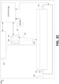
- FIG. 2C is a cross-sectional schematic side view of a substrate measurement subsystem 282, according to aspects of the present disclosure.
- Substrate measurement subsystem 282 may be configured to obtain measurements for one or more portions of a substrate, such as substrate 202 of FIG. 2A , prior to or after processing of substrate 202 at a processing chamber.
- Substrate measurement subsystem 282 may correspond to substrate measurement system 126 of FIG. 2A in embodiments.
- Substrate measurement subsystem 282 may obtain measurements for a portion of substrate 202 by generating data associated with the portion of substrate 202.
- substrate measurement subsystem 282 may be configured to generate spectral data, positional data, and/or other property data associated with substrate 202.
- the substrate measurement subsystem 282 may be configured to generate one or more types of data for the substrate, including spectral data, positional data, substrate property data, etc.
- the substrate measurement subsystem 282 can generate the data for the substrate in response to a request to obtain one or more measurements for the substrate before or after the substrate is processed at the manufacturing system.
- the substrate measurement subsystem 282 may include one or more components that facilitate the generation of data for the substrate.
- the substrate measurement subsystem can include a spectra sensing component for sensing spectra or spectrum from a portion of the substrate and generating spectral data for the substrate.
- the spectra sensing component can be an interchangeable component that can be configurable based on a type of process performed at the manufacturing system or a target type of measurements to be obtained at the substrate measurement subsystem.
- one or more components of the spectra sensing component can be interchanged at the substrate measurement subsystem to enable the collection of reflectometry spectral data, ellipsometry spectral data, hyperspectral imaging data, chemical imaging (e.g., x-ray photoelectron spectroscopy (XPS), energy-dispersive x-ray spectroscopy (EDX), (x-ray fluorescence (XRF), etc.) data, and so forth.
- XPS x-ray photoelectron spectroscopy
- EDX energy-dispersive x-ray spectroscopy
- XRF x-ray fluorescence
- Substrate measurement subsystem 282 may include a controller 283 configured to execute one or more instructions for generating data associated with a portion of substrate 202.
- Substrate measurement subsystem 282 may include a substrate sensing component 284 configured to detect when substrate 202 is transferred to substrate measurement subsystem 282.
- Substrate sensing component 284 may include any component configured to detect when substrate 202 is transferred to substrate measurement subsystem 282.
- substrate sensing component 284 may include an optical sensing component that transmits an optical beam across an entrance to substrate measurement subsystem 282.
- Substrate sensing component 284 may detect that a substrate 202 has been transferred to substrate measurement subsystem 282 responsive to substrate 202 breaking the optical beam transmitted across the entrance to substrate measurement subsystem 282 as substrate 202 is placed within substrate measurement subsystem 282. Responsive to detecting that substrate 202 has been transferred to substrate measurement subsystem 282, substrate sensing component 284 may transmit an indication to controller 283 indicating that substrate 202 has been transferred to substrate measurement subsystem 282.
- substrate sensing component 284 may be further configured to detect identifying information associated with substrate 202.
- substrate 202 may be embedded within a substrate carrier (not shown) when transferred to substrate measurement subsystem 282.
- the substrate carrier may include one or more registration features that enable identification of substrate 202.
- an optical sensing component of substrate sensing component 284 may detect that substrate 202, embedded within the substrate carrier, has broken the optical beam transmitted across the entrance to substrate measurement subsystem 282.
- the optical sensing component may further detect one or more registration features included on the substrate carrier. Responsive to detecting the one or more registration features, the optical sensing component may generate an optical signature associated with the one or more registration features.
- Substrate sensing component 284 may transmit the optical signature generated by the optical sensing component to controller 283 along with the indication that the substrate has been placed within substrate measurement subsystem 282. Responsive to receiving the optical signature from sensing component 284, controller 283 may analyze the optical signature to determine the identifying information associated with substrate 202.
- the identifying information associated with substrate 202 may include an identifier for substrate 202, an identifier for a process for substrate 202 (e.g., a batch number or a process run number), an identifier of a type for substrate 202 (e.g., a wafer, etc.), and so forth.
- Substrate measurement subsystem 282 may include one or more components configured to determine a position and/or an orientation of substrate 202 within substrate measurement subsystem 282.
- the position and/or orientation of substrate 202 may be determined based on an identification of a reference location of substrate 202.
- a reference location may be a portion of substrate 202 that includes an identifying feature that is associated with a specific portion of substrate 202.
- substrate 202 may have a reference tag embedded in a center portion of substrate 202.
- substrate 202 may have one or more structural features included on the surface of the substrate 202 at a center portion of substrate 202.
- Controller 283 may determine an identifying feature associated with a specific portion of substrate 202 based on determined identifying information for substrate 202. For example, responsive to determining that substrate 202 is a wafer, controller 283 may determine one or more identifying features that are generally included at a portion of a wafer.
- Controller 283 may identify the reference location for substrate 202 using one or more camera components 285 configured to capture image data for substrate 202. Camera components 285 may generate image data for with one or more portions of the substrate 202 and transmit the image data to controller 283. Controller 283 may analyze the image data to identify an identifying feature associated with a reference location for substrate 202. Controller 283 may further determine a position and/or orientation of substrate 202 as depicted in the image data based on the identified identifying feature of substrate 202. Controller 283 may determine a position and/or orientation of substrate 202 based on the identified identifying feature of substrate 202 and the determined position and/or orientation of substrate 202 as depicted in the image data.
- controller 283 may generate positional data associated with one or more portions of substrate 202.
- the positional data may include one or more coordinates (e.g., Cartesian coordinates, polar coordinates etc.) each associated with a portion of substrate 202, where each coordinate is determined based on a distance from the reference location for substrate 202.
- controller 283 may generate first positional data associated with a portion of substrate 202 that includes the reference location, where the first positional data includes a Cartesian coordinate of (0,0).
- Controller 283 may generate second positional data associated with a second portion of substrate 202 that is relative to the reference location.
- a portion of substrate 202 that is located approximately 2 nanometers (nm) due east of the reference location may be assigned a Cartesian coordinate of (0, 1).
- a portion of substrate 202 that is located 5 nms due north of the reference location may be assigned a Cartesian coordinate of (1,0).
- Controller 283 may determine one or more portions of substrate 202 to measure based on positional data determined for substrate 202. In some embodiments, controller 283 may receive one or more operations of a process recipe associated with substrate 202. In such embodiments, controller 283 may further determine the one or more portions of substrate 202 to measure based on one or more operations of the process recipe. For example, controller 283 may receive an indication that an etch process was performed for substrate 202 where several structural features were etched onto the surface of substrate 202. As a result, controller 283 may determine one or more structural features to measure and the expected locations of the features at various portions of substrate 202.
- Substrate measurement subsystem 282 may include one or more measurement components for measuring substrate 202.
- substrate measurement subsystem 282 may include one or more spectra sensing components 287 configured to generate spectral data for one or more portions of substrate 202.
- spectral data may correspond to an intensity (i.e., a strength or amount of energy) of a detected wave of energy for each wavelength of the detected wave.
- multiple wave lengths may be included in reflected energy waves received by substrate measurement subsystem 282. Each reflected energy wave may be associated with a different portion of substrate 202.
- an intensity may be measured for each reflected energy wave received by substrate measurement subsystem 282. Each intensity can be measured for each wavelength of reflected energy waves received by substrate measurement subsystem 282. The association between each intensity and each wavelength can be the basis for the formation of spectral data.
- one or more wavelengths can be associated with an intensity value that is outside of an expected range of intensity values. In such embodiments, the intensity value that is outside of the expected range of intensity values can be an indication that a defect exists at a portion of substrate 202.
- the measurement components for measuring substrate 202 can also include non-spectral sensing components configured to collect and generate non-spectral data.
- the measurement components can include an eddy current sensor or a capacitive sensor.
- some embodiments of the present description may refer to collecting and using spectral data for substrate 202, embodiments of the present description can be applicable to non-spectral data collected for substrate 202.
- a spectra sensing component 287 may be configured to detect waves of energy reflected from a portion of substrate 202 and generate spectral data associated with the detected waves.
- Spectra sensing component 287 may include a wave generator 288 and a reflected wave receiver 291.
- wave generator 288 may be a light wave generator configured to generate a beam of light towards a portion of substrate 202.
- reflected wave receiver 291 may be configured to receive a reflected light beam from the portion of substrate 202.
- Wave generator 288 may be configured to generate an energy stream 289 (e.g., a light beam) and transmit energy stream 289 to a portion of substrate 202.
- a reflected energy wave 290 may be reflected from the portion of substrate 202 and received by reflected wave receiver 291.
- FIG. 2C illustrates a single energy wave reflected off the surface of substrate 202, multiple energy waves may be reflected off the surface of substrate 202 and received by reflected wave receiver 291.
- spectra sensing component 287 may measure a wavelength of each wave included in reflected energy wave 289. Spectra sensing component 287 may further measure an intensity of each measured wavelength. Responsive to measuring each wavelength and each wavelength intensity, spectra sensing component 287 may generate spectral data for the portion of substrate 202. Spectra sensing component 287 may transmit the generated spectral data to controller 283. Controller 283 may, responsive to receiving the generated spectral data, generate a mapping between the received spectral data and positional data for the measured portion of substrate 202.
- Substrate measurement subsystem 282 may be configured to generate a specific type of spectral data based on a type of measurement to be obtained at substrate measurement subsystem 282.
- spectra sensing component 287 may be a first spectra sensing component that is configured to generate one type of spectral data.
- spectra sensing component 287 may be configured to generate reflectometry spectral data, ellipsometry spectral data, hyperspectral imaging data, chemical imaging data, thermal spectral data, or conductive spectral data.
- Controller 283 may determine a type of data (i.e., spectral data, non-spectral data) to be generated for substrate 202 based on a type of measurement to be obtained for one or more portions of substrate 202. In some embodiments, controller 283 may determine the one or more types of measurements based on a notification received from system controller 228 of FIG. 2A . In other or similar embodiments, controller 283 may determine the one or more types of measurements based on an instruction to generate a measurement for a portion of substrate 202. Responsive to determining the one or more types of measurements to be obtained, controller 283 may determine the type of data to be generated for substrate 202.
- a type of data i.e., spectral data, non-spectral data
- controller 283 can determine that spectral data is to be generated for substrate 202 and that the second spectra sensing component is an optimal sensing component for obtaining the determined type of measurements for the one or more portions of substrate 202. Responsive to determining the second sensing component is the optimal sensing component, controller 283 may transmit a notification to the system controller indicating that the first spectra sensing component should be replaced with the second spectra sensing component and the second spectra sensing component should be used to obtain the one or more types of measurements for the one or more portions of substrate 202. System controller 128 may transmit the notification to a client device connected to the manufacturing system where the client device may provide the notification to a user of the manufacturing system (e.g., an operator) via a GUI.
- a user of the manufacturing system e.g., an operator
- spectra sensing component 287 may be configured to generate multiple types of spectral data.
- controller 283 may cause spectra sensing component 287 to generate a specific type of spectral data based on the type of measurements to be obtained for one or more portions of substrate 202, in accordance with previously described embodiments. Responsive to determining the type of measurements to be obtained, controller 283 may determine that a first type of spectral data is to be generated by spectra sensing component 287. Based on the determination that the first type of spectral data is to be generated by spectra sensing component 287, controller 283 may cause spectra sensing component 287 to generate the first type of spectral data for the one or more portions of substrate 202.
- controller 283 may determine one or more portions of substrate 202 to measure at substrate measurement subsystem 282.
- one or more measurement components such as spectra sensing component 287
- substrate measurement subsystem 282 may include one or more positional components 295 configured to modify a position and/or an orientation of substrate 202 with respect to spectra sensing component 287.
- positional components 295 may be configured to translate substrate 202 along a first axis and or a second axis, relative to spectra sensing component 287.
- positional components 295 may be configured to rotate substrate 202 around a third axis relative to spectra sensing component 287.
- positional components 295 may modify the position and/or orientation of substrate 202 in accordance with the one or more determined portions to be measured for substrate 202. For example, prior to spectra sensing component 287 generating spectral data for substrate 202, positional components 295 may position substrate 202 at Cartesian coordinate (0,0) and spectra sensing component 287 may generate first spectral data for substrate 202 at Cartesian coordinate (0,0).
- positioning components 240 may translate substrate 202 along a first axis so that spectra sensing component 287 is configured to generate second spectral data for substrate 202 at Cartesian coordinate (0,1).
- controller 283 may rotate substrate 202 along a second axis so that spectra sensing component 287 is configured to generate third spectral data for substrate 202 at Cartesian coordinate (1,1). This process may occur multiple times until spectral data is generated for each determined portion of substrate 202.
- Manufacturing equipment 122 can be coupled to server machine 320.
- Server machine 320 can include processing device 322 and/or data store 332.
- processing device 322 can be configured to execute one or more instructions to perform operations at manufacturing equipment 122.
- processing device 322 can include or be a part of system controller 228, described with respect to FIG. 2A .
- Data store 332 can include or be part of data store 150 and/or data store 250, in some embodiments.
- the substrate placement metrics may be compared against a known pattern and/or combination of substrate placement metrics (e.g., target substrate placement metrics).
- Target substrate placement metrics may be associated with an ideal substrate placement for optimal processing of the substrate.
- substrate placement engine 330 can determine a recommended placement for substrates to be processed and/or may provide an alert to a user.
- Substrate placement criteria may include a specified combination of values indicated by the substrate placement metrics in some embodiments.
- processing device 322 can include a training set generator 324 and/or a training engine 326, in some embodiments.
- training set generator 324 can correspond to training set generator 172 and/or training engine 326 can correspond to training engine 182, described with respect to FIG. 1 .
- Training set generator 324 can be configured to generate training sets 340 to train machine learning model 334 or a set of machine learning models 334.
- training set generator 324 can generate a training input based on historical substrate surface profile data 336.
- the substrate surface profile data 336 (e.g., thickness profile maps) may be associated with etch rates and/or tilt across the surface of one or more substrates processed in a processing chamber.
- training set generator 324 can retrieve the historical substrate surface profile data 336 (e.g., substrate thickness profile data) from data store 332 to generate the training input.
- Training set generator 324 can generate a target output indicating an estimated substrate placement value (e.g., substrate placement metrics) for the training input based on historical substrate surface profile data 336.
- Training set generator 324 can include the generated training input and the generated target output in a training set 340.
- the training set 340 may additionally include, for each historical substrate thickness profile, an indicator of substrate placement (e.g., on a substrate support such as an electrostatic chuck relative to an inner diameter of a process kit ring). Further details regarding generating training set 340 are provided with respect to FIG. 5 .
- Training engine 326 can be configured to train, validate and/or test the machine learning model 334 or sets of machine learning models 334. Training engine 326 can provide training set 340 to train machine learning model(s) 334 and store trained machine learning model(s) 334 at data store 332. In some embodiments, training engine 326 can use a validation set 342 to validate a trained machine learning model 334. Validation set 342 can include surface profile data 336 and associated chamber component condition metrics. Training set generator 324 and/or training engine 326 can generate validation set 342 based on historical surface profile data 336. In some embodiments, validation set 342 can include historical surface profile data 336 that is different from historical surface profile data 336 included in training set 340.
- Training engine 326 can provide the historical surface profile data 336 as an input to a trained machine learning model 334 and can extract one or more substrate placement metric(s) for processing a substrate in a processing chamber from one or more outputs of the trained model 334.
- the input may additionally include ages of one or more components of the processing chamber and/or one or more images of a substrate that was used to generate the historical surface profile data 236.
- Training engine 326 can assign a performance score to the trained model 334 based on an accuracy of the substrate placement metric(s).
- Training engine 326 can select the trained model 334 to be used to assess the substrate placement for processing the substrate in a process chamber based on surface profile data for a substrate processed by the process chamber.
- a user of manufacturing system 200 may be provided with access to data stored at one or more portions of data store 332 or one or more processes executed at processing device 322. However, the user of manufacturing system 200 may not be provided with access to any data stored at one or more portions of data store 354 or any processes executed at processing device 352.
- Processing device 352 can be configured to execute training set generator 324 and/or training engine 326 in a similar fashion as processing device 322.
- server 350 can be coupled to manufacturing equipment 122 and/or inline metrology equipment 130 via a network.
- processing device 352 can obtain surface profile data 336 and substrate placement metrics corresponding to surface profile data 336 to be used by training set generator 324 and/or training engine 326 to generate training set 340 and validation set 342, in accordance with embodiments described with respect to processing device 322.
- server 350 is not coupled to manufacturing equipment 122 and/or external metrology equipment 130. Accordingly, processing device 352 can surface profile data 336 from processing device 322.
- Training set generator 324 at processing device 352 can generate training set 340 in accordance with previously described embodiments. Training engine 326 at processing device 352 can train and/or validate machine learning model 334, in accordance with previously described embodiments.
- server 350 can be coupled to other manufacturing equipment and/or other server machines that are different from manufacturing equipment 122 and/or server machine 320. Processing device 352 can obtain surface profile data 336 from the other manufacturing equipment and/or server machines, in accordance with embodiments described herein.
- training set 340 and/or validation set 342 can be generated based on surface profile data 336 obtained for substrates processed at process chamber 310 as well as other surface profile data obtained for other substrates processed at process chambers at other manufacturing systems.
- FIG. 4 illustrates a model training workflow 405 and a model application workflow 417 for substrate placement determination according to one embodiment.
- Model training workflow 405 and model application workflow 417 may be performed by processing logic executed by a processor of a computing device.
- One or more of these workflows 405, 417 may be implemented, for example, by one or more machine learning models implemented on a processing device and/or other software and/or firmware executing on a processing device.
- one or more machine learning models are trained to perform one or more substrate placement estimation tasks. Each task may be performed by a separate machine learning model. Alternatively, a single machine learning model may perform each of the tasks or a subset of the tasks. For example, a first machine learning model may be trained to determine a substrate placement (e.g., a location on a substrate support for substrate processing), and a second machine learning model may be trained to determine a substrate handoff offset (e.g., a substrate handling robot handoff offset). Additionally, or alternatively, different machine learning models may be trained to perform different combinations of the tasks.
- a substrate placement e.g., a location on a substrate support for substrate processing
- a substrate handoff offset e.g., a substrate handling robot handoff offset
- Training of a neural network may be achieved in a supervised learning manner, which involves feeding a training dataset consisting of labeled inputs through the network, observing its outputs, defining an error (by measuring the difference between the outputs and the label values), and using techniques such as deep gradient descent and backpropagation to tune the weights of the network across all its layers and nodes such that the error is minimized.
- a supervised learning manner which involves feeding a training dataset consisting of labeled inputs through the network, observing its outputs, defining an error (by measuring the difference between the outputs and the label values), and using techniques such as deep gradient descent and backpropagation to tune the weights of the network across all its layers and nodes such that the error is minimized.
- a training dataset containing hundreds, thousands, tens of thousands, hundreds of thousands or more profile maps 412 of a substrate should be used to form a training dataset.
- Data may include, for example, a uniformity profile determined using a given number of measurements each associated with a particular target position. This data may be processed to generate one or more training datasets 436 for the training of one or more machine learning models.
- Training data items in training datasets 436 may include profile maps 412, substrate placements used to process substrates that were measured to generate the profile maps, and/or one or more images of the substrates.
- processing logic inputs the training dataset(s) 436 into one or more untrained machine learning models.
- the machine learning model Prior to inputting a first input into a machine learning model, the machine learning model may be initialized.
- Processing logic trains the untrained machine learning model(s) based on the training dataset(s) to generate one or more trained machine learning models that perform various operations as set forth above. Training may be performed by inputting input data such as one or more profile maps 412 (e.g., thickness profile maps, spectra profile maps, roughness profile maps, particle count profile maps, optical constant profile maps, etc.), images and/or age information of components into the machine learning one at a time.
- profile maps 412 e.g., thickness profile maps, spectra profile maps, roughness profile maps, particle count profile maps, optical constant profile maps, etc.
- An artificial neural network includes an input layer that consists of values in a data point.
- the next layer is called a hidden layer, and nodes at the hidden layer each receive one or more of the input values.
- Each node contains parameters (e.g., weights) to apply to the input values.
- Each node therefore essentially inputs the input values into a multivariate function (e.g., a non-linear mathematical transformation) to produce an output value.
- a next layer may be another hidden layer or an output layer. In either case, the nodes at the next layer receive the output values from the nodes at the previous layer, and each node applies weights to those values and then generates its own output value. This may be performed at each layer.
- a final layer is the output layer, where there is one node for each class, prediction and/or output that the machine learning model can produce.
- the output may include one or more predictions or inferences (e.g., estimations of substrate placement in a process chamber for substrate processing in a process chamber in which a measured substrate was processed).
- Processing logic may compare the output estimated substrate placement(s) against historical substrate placement(s).
- Processing logic determines an error (i.e., a classification error) based on the differences between the estimated substrate placement(s) and the target substrate placement(s).
- Processing logic adjusts weights of one or more nodes in the machine learning model based on the error.
- An error term or delta may be determined for each node in the artificial neural network. Based on this error, the artificial neural network adjusts one or more of its parameters for one or more of its nodes (the weights for one or more inputs of a node).
- model validation may be performed to determine whether the model has improved and to determine a current accuracy of the deep learning model.
- processing logic may determine whether a stopping criterion has been met.
- a stopping criterion may be a target level of accuracy, a target number of processed images from the training dataset, a target amount of change to parameters over one or more previous data points, a combination thereof and/or other criteria.
- the stopping criteria is met when at least a minimum number of data points have been processed and at least a threshold accuracy is achieved.
- the threshold accuracy may be, for example, 70%, 40% or 90% accuracy.
- the stopping criterion is met if accuracy of the machine learning model has stopped improving.
- input data 462 may be input into one or more substrate placement determiners 467, each of which may include a trained neural network or other model. Additionally, or alternatively, one or more substrate placement determiner 467 may apply image processing algorithms to determine chamber component conditions.
- the input data may include a profile map (e.g., of a polymer layer on a substrate measured using an integrated reflectometry device or substrate measurement system).
- the input data may additionally optionally include one or more images of the substrate.
- substrate placement determiner(s) 467 may output one or more estimated substrate placement(s) 469.
- processing logic determines if a stopping criterion is met. If a stopping criterion has not been met, the method returns to block 610, and another training data item is input into the machine learning model. If a stopping criterion is met, the method proceeds to block 625, and training of the machine learning model is complete.
- the process chamber processes the substrate.
- the process chamber may perform an etch process to partially remove a film on the surface of the substrate or a film deposition process to deposit a film on the substrate.
- the film is a polymer.
- the film is a ceramic (e.g., a metal oxide).
- the processing of the substrate may be performed according to a recipe (e.g., an etch process recipe, a deposition process recipe, etc.).
- the substrate may be supported by a substrate support of the process chamber (e.g., an electrostatic chuck).
- the substrate may be placed at an initial position in the process chamber prior to the processing (e.g., at block 708) and may remain in the initial position during the processing.
- the substrate includes a surface profile (e.g., a thickness profile, etc.).
- one or more robots transfers the substrate from the process chamber to a substrate measurement system. If the substrate measurement system is connected to or included in a transfer chamber, then a transfer chamber robot may remove the substrate from the process chamber and insert the substrate into the substrate measurement system. If the substrate measurement system is connected to or included in a factory interface, then a transfer chamber robot may remove the substrate from the process chamber and place the substrate in a load lock. A factory interface robot may then remove the substrate from the load lock and insert the substrate into the substrate measurement system.
- the substrate measurement system may be any of the aforementioned substrate measurement systems, such as an integrated reflectometry (IR) device.
- IR integrated reflectometry
- the substrate measurement system generates measurements of many locations on a surface of the substrate. Each location may have a unique set of coordinates.
- the substrate measurement system and/or a computing device may generate a profile map of the surface profile of the substrate (e.g., a substrate surface profile map) based on the measurements of the substrate measurement system.
- the profile map may be or include an image, where each pixel in the image corresponds to a coordinate on the substrate. Each pixel may have an intensity value that corresponds to a measurement value (e.g., thickness value) at the coordinate of the substrate associated with the pixel.
- the profile map is indicative of a thickness profile, which is indicative of an etch rate profile.
- the profile map may reflect a thickness profile of the substrate having undergone an etch process for a predetermined amount of time.
- the profile map is indicative of substrate surface defects such as tilt.
- Tilt is correlated to etch rate, in some embodiments.
- the profile may be or include a feature vector, where each entry in the feature vector is associated with a coordinate of the substrate, and where each entry may have a value that represents a value of the surface profile at the coordinate of the substrate.
- the processing logic e.g., of the measurement system and/or of the computing device may determine an etch rate profile map corresponding to an etch rate proximate the edge of the substrate.
- the model is a physics-based model or a statistical model.
- the model outputs an estimated substrate placement value (e.g., an estimated substrate placement metric) for placement of the substrate relative to one or more components of the substrate support.
- the model outputs a placement metric of the substrate (e.g., a coordinate position of the substrate on the substrate support) that corresponds to a placement relative to the substrate support (e.g., the electrostatic chuck) and/or one or more components of the substrate support (e.g., the process kit ring).
- the output of the model is based on the etch rate profile map determined at block 716.
- the output of the model indicates that the substrate was not placed in an optimal position for the processing.
- one or more computer vision algorithms are used to process the profile map(s).
- a substrate e.g., a second substrate
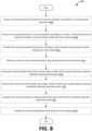
- processing logic causes a robot to place the substrate on a substrate support (e.g., an electrostatic chuck) within the process chamber.
- the robot may place the substrate at a position such that the center of the substrate is offset from the center of the substrate support, according to the recommended placement.
- the recommended placement may specify that the center of the substrate is to be offset from the center of the electrostatic chuck a specified amount in a specified direction.
- the amount and direction of the offset may be the difference between a first robot handoff orientation and a second robot handoff orientation.
- the first robot handoff orientation is a baseline (e.g., default, etc.) orientation
- the second robot handoff orientation is an updated orientation based on the offset.
- the robot may place the substrate on the electrostatic chuck the specified amount of the offset from the center of the electrostatic chuck in the direction of the offset.
- the substrate is transferred (e.g., by one or more transfer robots) from the process chamber to a substrate measurement system (e.g., similar to at block 712 of method 700).
- a computing device processes data from the profile map (e.g., thickness profile map, particle map, optical constant map, roughness map, etc.) using a model (e.g., a trained machine learning model, a physics-based model, a statistical model, etc.).
- the model outputs an estimated substrate placement value (e.g., an estimated substrate placement metric, etc.).
- processing logic updates the recommended placement based on the comparing at block 820.
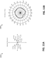
- plot diagram 1100A of a substrate placement DOE is shown.
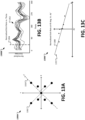
- FIG. 13A an example plot diagram 1300A illustrating substrate placement in a DOE is shown.
- plot diagram 1100A may correspond with plot diagram 1300A.
- substrates may be placed at various locations on the substrate support for performing the DOE.
- a substrate is placed and processed at each of the placement locations 1102-1118.
- location 1118 may correspond to a center of a substrate support.
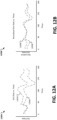
- etch rates are determined for several azimuthal angles about the center of a processed substrate such that the determined etch rates are representative of the entire etch rate profile.
- the determined etch rates may be only representative of all the azimuthal angles.
- etch rates can be determined at azimuthal angles of 0°, 15°, 30°, 45°, etc. around the processed substrate proximate the edge of the substrate.
- etch rates can be determined at various azimuthal angles of different graduations than illustrated in FIG. 11B .
- etch rates can be determined at 0°, 10°, 20°, 30°, etc. or 0°, 30°, 60°, 95°, etc.
- FIG. 11B shows the etch rates of a processed substrate at various azimuthal angles about the center of the substrate near the edge of the substrate.
- Each value of the first etch rate profile is divided by the first average etch rate to determine a first normalized etch rate profile.
- a second average etch rate is determined for a second etch rate profile.
- Each value of the second etch rate profile is divided by the second average etch rate to determine a second normalized etch rate profile.
- Other methods of normalizing the etch rate data may be used. More details regarding data normalization are discussed herein below with respect to FIG. 10B .
- Normalized etch rates 1372 for each processed substrate at azimuthal angle 1354 are plotted with respect to a differential position along a vector 1310 of FIG. 13A . More details regarding vector 1310 of FIG. 13A are described herein below.
- a linear fit 1380 is formed through the plotted normalized etch rates 1372.
- the linear fit 1380 may represent a predicted etch rate of a processed substrate at various positions along the vector 1310 at the corresponding azimuthal angle.
- a linear fit may be determined for the normalized etch rates at each azimuthal angle.
- an optimal substrate placement location is determined.
- an etch rate profile can be predicted for any substrate placement using the linear fit data.
- an optimal location can be determined that satisfies one or more metrics. For example, a placement location can be determined that minimizes an etch rate range (e.g., etch rate range proximate the edge of a substrate) or an etch rate standard deviation (e.g., etch rate standard deviation proximate the edge of a substrate). Minimizing the etch rate range and/or etch rate standard deviation can result in more consistently-processed substrates, particularly near the edge of the substrate.
- the optimal placement is recommended to the substrate processing system.
- a substrate can be caused to be placed on a substrate support in a process chamber according to the recommended placement.
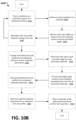
- a substrate is placed at a placement location on a substrate support.
- the substrate may be a test substrate that is to be processed as part of a DOE.
- the substrate may be placed at one of the locations 1102-1118 shown in FIG. 11A .
- an etch operation may be performed on the substrate to remove material from the substrate (or a deposition operation may be performed to add material to the substrate).
- etch rate or deposition rate may be measured proximate the edge of the substrate at a radial distance from the center of the substrate at multiple azimuthal angles.
- etch rate or deposition rate is measured at a distance between approximately 140 mm and 150 mm from the center of the substrate about the center axis of the substrate.
- An etch rate profile or deposition rate profile (e.g., shown in FIG. 11B for a single substrate and shown in FIG. 12A for two substrates) can be constructed using the measured etch rates or deposition rates at the various azimuthal angles.
- the etch rate profile or deposition rate profile is normalized. In some embodiments, the etch rate profile or deposition rate profile is normalized using an average etch rate for the etch rate profile or an average deposition rate for the deposition rate profile. For example, referring to FIG.
- an average etch rate may be determined from azimuthal angle 0° to azimuthal angle 360°.
- Each value of etch rate over the etch rate profile may be divided by the average etch rate to calculate a normalized etch rate profile 1202B of FIG. 12B .
- blocks 1010-1040 can be repeated multiple times for multiple substrates processed as part of the DOE. Each time block 1010 is repeated, the associated substrate is placed at a different placement location on the substrate support. In some embodiments, blocks 1010-1040 are repeated nine times to process nine test substrates at nine different placement locations. In some embodiments, blocks 1010-1040 are repeated as few as three time to process as few as three test substrates at as few as three different placement locations. Including more or fewer substrates in the DOE (and thus repeating blocks 1010-1040 more or fewer times) is dependent on an accuracy threshold of the DOE. For example, if the accuracy threshold is higher, more test substrates are processed. Similarly, if the accuracy threshold is lower, fewer test substrate may be processed.
- the normalized etch rate profiles for each of the substrates processed at blocks 1010-1040 are compiled.
- a graphical representation 1300B of the normalized etch rate profiles is shown.
- the normalized etch rate profiles 1352 may be representative of the etch rate profiles for substrates processed at each placement location 1102-118 shown in FIG. 11A and/or each placement location 1302 shown in FIG. 13A .
- a normalized etch rate at each azimuthal angle for each processed substrate is determined. Referring to FIG.
- a normalized etch rate is determined from a corresponding normalized etch rate profile 1352 at an azimuthal angle 1354.
- Azimuthal angle 1354 is illustrated at 45°.
- several normalized etch rates for each processed substrate are determined from the normalized etch rate profiles 1352 at all azimuthal angles depending on how dense the substrate etch rate sampling map is.
- a linear fitment is made.
- the linear fitment can be made using various linear and nonlinear higher order fitment methods known to those in the art.
- FIG. 13A an example plot diagram 1300A illustrating substrate placement in a DOE is shown. Substrates may be processed while placed at each of the substrate placement locations 1302 on the substrate support.
- a vector 1310 may correspond to azimuthal angle 1354 of FIG. 13B .
- the vector 1310 may be at an angle to the X-axis equivalent to the value of the azimuthal angle 1354.
- the placement locations 1302 may be projected onto vector 1310 and the location of each of the projected placement locations on the vector 1310 are translated to a value y'.
- y' is at an angle of 45° from the X axis of plot 1300A
- azimuthal angle 1354 is similarly at a corresponding angle theta of 45°.
- normalized etch rates 1372 at the azimuthal angle 1354 are shown with respect to dy'.
- a normalized etch rate 1372 is plotted for each of the processed substrates.
- a linear fit 1380 is calculated to fit the plotted normalized etch rates 1372.
- the process of projecting placement locations 1302 onto a vector 1310, translating the location of each of the projected placement locations onto the vector 1310 to y', and plotting normalized etch rates 1372 with respect to dy' may be repeated for each of the data corresponding to each of the several azimuthal angles.
- a predicted etch rate profile is calculated for an estimated substrate placement location.
- an estimated location may be determined that may produce a substrate meeting one or more threshold criterion.
- the threshold criterion may include a threshold etch rate profile range, a threshold etch rate profile minimum, a threshold etch rate profile maximum, and/or a threshold etch rate profile standard deviation.
- a predicted value of etch rate at a specific azimuthal angle can be calculated for an estimated substrate placement location using the linear fit 1380 corresponding to the specific azimuthal angle.
- etch rate profile 1202A is the etch rate profile of a substrate processed at an optimal location on a substrate support.
- the optimal location may be determined using one or more methods described herein.
- etch rate profile 1204A is the etch rate profile of a substrate processed at a non-optimal location on a substrate support.
- normalized etch rate profile 1202B is the normalized etch rate profile of a substrate processed at an optimal location on a substrate support.
- normalized etch rate profile 1204B is the normalized etch rate profile of a substrate processed at a non-optimal location on a substrate support.
- the normalized etch rate profile 1202B has a more consistent normalized etch rate across all azimuthal angles theta. Therefore, the etch rates of the substrate processed at the optimal location are more consistent and processing substrates at the optimal location will yield better substrates than processing substrates at non-optimal locations.
- FIG. 14 is a flow diagram for a method 1400 of determining an optimal substrate placement, according to aspects of the present disclosure.
- Method 1400 may be performed by processing logic that can include hardware (circuitry, dedicated logic, etc.), software (such as is run on a general purpose computer system or a dedicated machine), firmware, or some combination thereof.
- method 1400 can be performed by a computer system, such as computer system architecture 100 of FIG. 1 .
- one or more operations of method 1400 can be performed by one or more other machines not depicted in the figures.
- a first substrate is processed in a process chamber.
- the process chamber may perform an etch process to partially remove a film on the surface of the substrate or a film deposition process to deposit a film on the substrate.
- the film is a polymer.
- the film is a ceramic (e.g., a metal oxide).
- the processing of the substrate may be performed according to a recipe (e.g., an etch process recipe, a deposition process recipe, etc.).
- the substrate may be supported by a substrate support of the process chamber (e.g., an electrostatic chuck).
- the substrate may be placed at an initial position in the process chamber prior to the processing and may remain in the initial position during the processing.
- the substrate includes a surface profile (e.g., a thickness profile, etc.).
- one or more robots transfers the substrate from the process chamber to a substrate measurement system. If the substrate measurement system is connected to or included in a transfer chamber, then a transfer chamber robot may remove the substrate from the process chamber and insert the substrate into the substrate measurement system. If the substrate measurement system is connected to or included in a factory interface, then a transfer chamber robot may remove the substrate from the process chamber and place the substrate in a load lock. A factory interface robot may then remove the substrate from the load lock and insert the substrate into the substrate measurement system.
- the substrate measurement system may be any of the aforementioned substrate measurement systems, such as an integrated reflectometry (IR) device.
- IR integrated reflectometry
- the substrate measurement system generates measurements for many locations on a surface of the substrate. Each location may have a unique set of coordinates.
- the substrate measurement system and/or a computing device may generate a profile map of the surface profile of the substrate (e.g., a substrate surface profile map) based on the measurements of the substrate measurement system.
- the profile map may be or include an image, where each pixel in the image corresponds to a coordinate on the substrate. Each pixel may have an intensity value that corresponds to a measurement value (e.g., thickness value) at the coordinate of the substrate associated with the pixel.
- the profile map is indicative of a thickness profile, which is indicative of an etch rate profile.
- the profile map may reflect a thickness profile of the substrate having undergone an etch process for a predetermined amount of time.
- the profile map is indicative of substrate surface defects such as tilt.
- processing logic processes data associated with the plurality of etch rates determined at block 1418.
- the computing device uses a model to process the data.
- the model may include a trained machine learning model, a mathematical model, a linear fitment model, and/or a statistical model.
- the model may output one or more estimated surface profiles associated with one or more estimated placement locations on the substrate support. For example, the model may use numerical methods to estimate a predicted surface profile for a substrate processed at an estimated placement location.
- the model normalizes the etch rate profile (e.g., determined at block 1418) and determines a normalized etch rate a various values of azimuthal angle theta.
- processing logic determines a recommended placement for substrates on the substrate support based on the one or more estimated placement locations (e.g., output by the model at block 1420).
- the computing device may determine a location on the substrate support for placement of the substrate using the estimated placement locations.
- the computing device may determine a coordinate position based or a value (or values) output from the model at block 1420.
- the processing logic may then cause another substrate to be placed in the process chamber (e.g., via a substrate-handling robot) according to the recommended placement as described herein.
Landscapes
- Engineering & Computer Science (AREA)
- Physics & Mathematics (AREA)
- Theoretical Computer Science (AREA)
- Software Systems (AREA)
- General Physics & Mathematics (AREA)
- Evolutionary Computation (AREA)
- Artificial Intelligence (AREA)
- Computing Systems (AREA)
- Mathematical Physics (AREA)
- General Engineering & Computer Science (AREA)
- Data Mining & Analysis (AREA)
- General Health & Medical Sciences (AREA)
- Health & Medical Sciences (AREA)
- Molecular Biology (AREA)
- Life Sciences & Earth Sciences (AREA)
- Biomedical Technology (AREA)
- Biophysics (AREA)
- Computational Linguistics (AREA)
- Computer Vision & Pattern Recognition (AREA)
- Plasma & Fusion (AREA)
- Medical Informatics (AREA)
- Chemical & Material Sciences (AREA)
- Analytical Chemistry (AREA)
- Multimedia (AREA)
- Quality & Reliability (AREA)
- Databases & Information Systems (AREA)
- Container, Conveyance, Adherence, Positioning, Of Wafer (AREA)
- Drying Of Semiconductors (AREA)
- Automation & Control Theory (AREA)
Applications Claiming Priority (4)
| Application Number | Priority Date | Filing Date | Title |
|---|---|---|---|
| US17/822,009 US20240069537A1 (en) | 2022-08-24 | 2022-08-24 | Substrate placement optimization using substrate measurements |
| US18/200,921 US20240071838A1 (en) | 2022-08-24 | 2023-05-23 | Substrate placement optimization using substrate measurements |
| PCT/US2023/030866 WO2024044215A1 (en) | 2022-08-24 | 2023-08-22 | Substrate placement optimization using substrate measurements |
| EP23858008.8A EP4573591A1 (de) | 2022-08-24 | 2023-08-22 | Substratplatzierungsoptimierung unter verwendung von substratmessungen |
Related Parent Applications (2)
| Application Number | Title | Priority Date | Filing Date |
|---|---|---|---|
| EP23858008.8A Division EP4573591A1 (de) | 2022-08-24 | 2023-08-22 | Substratplatzierungsoptimierung unter verwendung von substratmessungen |
| EP23858008.8A Division-Into EP4573591A1 (de) | 2022-08-24 | 2023-08-22 | Substratplatzierungsoptimierung unter verwendung von substratmessungen |
Publications (2)
| Publication Number | Publication Date |
|---|---|
| EP4579722A2 true EP4579722A2 (de) | 2025-07-02 |
| EP4579722A3 EP4579722A3 (de) | 2025-11-12 |
Family
ID=89997776
Family Applications (2)
| Application Number | Title | Priority Date | Filing Date |
|---|---|---|---|
| EP25152275.1A Pending EP4579722A3 (de) | 2022-08-24 | 2023-08-22 | Substratplatzierungsoptimierung unter verwendung von substratmessungen |
| EP23858008.8A Pending EP4573591A1 (de) | 2022-08-24 | 2023-08-22 | Substratplatzierungsoptimierung unter verwendung von substratmessungen |
Family Applications After (1)
| Application Number | Title | Priority Date | Filing Date |
|---|---|---|---|
| EP23858008.8A Pending EP4573591A1 (de) | 2022-08-24 | 2023-08-22 | Substratplatzierungsoptimierung unter verwendung von substratmessungen |
Country Status (7)
| Country | Link |
|---|---|
| US (1) | US20240071838A1 (de) |
| EP (2) | EP4579722A3 (de) |
| JP (2) | JP2025529627A (de) |
| KR (2) | KR20250027849A (de) |
| CN (2) | CN120048761A (de) |
| TW (1) | TW202425215A (de) |
| WO (1) | WO2024044215A1 (de) |
Families Citing this family (1)
| Publication number | Priority date | Publication date | Assignee | Title |
|---|---|---|---|---|
| US20260101723A1 (en) * | 2024-10-08 | 2026-04-09 | Applied Materials, Inc. | Interactive user interface for substrate edge profile |
Family Cites Families (22)
| Publication number | Priority date | Publication date | Assignee | Title |
|---|---|---|---|---|
| JP4731755B2 (ja) * | 2001-07-26 | 2011-07-27 | 東京エレクトロン株式会社 | 移載装置の制御方法および熱処理方法並びに熱処理装置 |
| US7381576B2 (en) * | 2005-08-15 | 2008-06-03 | Infineon Technologies Richmond, Lp. | Method and apparatus for monitoring precision of water placement alignment |
| JP2007150070A (ja) * | 2005-11-29 | 2007-06-14 | Shin Etsu Handotai Co Ltd | 半導体ウエーハのプラズマエッチング方法 |
| US7486878B2 (en) * | 2006-09-29 | 2009-02-03 | Lam Research Corporation | Offset correction methods and arrangement for positioning and inspecting substrates |
| US7479236B2 (en) * | 2006-09-29 | 2009-01-20 | Lam Research Corporation | Offset correction techniques for positioning substrates |
| US8135485B2 (en) * | 2007-09-28 | 2012-03-13 | Lam Research Corporation | Offset correction techniques for positioning substrates within a processing chamber |
| KR101341371B1 (ko) * | 2008-11-18 | 2013-12-13 | 도쿄엘렉트론가부시키가이샤 | 플라즈마 처리 장치 및 플라즈마 처리 방법 |
| CN103081073B (zh) * | 2010-11-30 | 2015-12-02 | 佳能安内华股份有限公司 | 等离子体处理设备 |
| JP5913829B2 (ja) * | 2011-04-21 | 2016-04-27 | 株式会社日立ハイテクノロジーズ | プラズマ処理装置 |
| JP6196833B2 (ja) * | 2012-09-26 | 2017-09-13 | 株式会社日立国際電気 | 半導体装置の製造方法、基板処理装置およびプログラム |
| US9792393B2 (en) * | 2016-02-08 | 2017-10-17 | Lam Research Corporation | Methods and apparatuses for etch profile optimization by reflectance spectra matching and surface kinetic model optimization |
| US10032681B2 (en) * | 2016-03-02 | 2018-07-24 | Lam Research Corporation | Etch metric sensitivity for endpoint detection |
| US10971333B2 (en) * | 2016-10-24 | 2021-04-06 | Samsung Electronics Co., Ltd. | Antennas, circuits for generating plasma, plasma processing apparatus, and methods of manufacturing semiconductor devices using the same |
| JP7141892B2 (ja) * | 2018-09-03 | 2022-09-26 | 株式会社プレテック | エッチング装置及びエッチング方法 |
| JP7224254B2 (ja) * | 2019-07-17 | 2023-02-17 | 東京エレクトロン株式会社 | 基板処理装置、情報処理装置、及び基板処理方法 |
| US11328944B2 (en) * | 2019-10-23 | 2022-05-10 | Eugenus, Inc. | Systems and methods of placing substrates in semiconductor manufacturing equipment |
| JP7412150B2 (ja) * | 2019-11-29 | 2024-01-12 | 東京エレクトロン株式会社 | 予測装置、予測方法及び予測プログラム |
| JP2022018205A (ja) * | 2020-07-15 | 2022-01-27 | 東京エレクトロン株式会社 | 異常検知方法及び異常検知装置 |
| US20220026817A1 (en) * | 2020-07-22 | 2022-01-27 | Applied Materials, Inc. | Determining substrate profile properties using machine learning |
| US12332625B2 (en) * | 2020-09-21 | 2025-06-17 | Changxin Memory Technologies, Inc. | Method and apparatus for correcting position of wafer and storage medium |
| US20250021015A1 (en) * | 2021-11-17 | 2025-01-16 | Asml Netherlands B.V. | Determining an etch effect based on an etch bias direction |
| CN114843182B (zh) * | 2022-04-14 | 2025-08-08 | 江西乾照光电有限公司 | 一种晶圆刻蚀方法 |
-
2023
- 2023-05-23 US US18/200,921 patent/US20240071838A1/en active Pending
- 2023-08-22 WO PCT/US2023/030866 patent/WO2024044215A1/en not_active Ceased
- 2023-08-22 EP EP25152275.1A patent/EP4579722A3/de active Pending
- 2023-08-22 KR KR1020257005090A patent/KR20250027849A/ko active Pending
- 2023-08-22 KR KR1020257005030A patent/KR20250037546A/ko active Pending
- 2023-08-22 JP JP2025500946A patent/JP2025529627A/ja active Pending
- 2023-08-22 EP EP23858008.8A patent/EP4573591A1/de active Pending
- 2023-08-22 CN CN202510130437.5A patent/CN120048761A/zh active Pending
- 2023-08-22 CN CN202380056621.9A patent/CN119604973B/zh active Active
- 2023-08-24 TW TW112131823A patent/TW202425215A/zh unknown
-
2025
- 2025-03-31 JP JP2025058341A patent/JP2025107174A/ja active Pending
Also Published As
| Publication number | Publication date |
|---|---|
| JP2025107174A (ja) | 2025-07-17 |
| KR20250027849A (ko) | 2025-02-27 |
| JP2025529627A (ja) | 2025-09-09 |
| CN119604973A (zh) | 2025-03-11 |
| CN119604973B (zh) | 2025-12-19 |
| TW202425215A (zh) | 2024-06-16 |
| WO2024044215A1 (en) | 2024-02-29 |
| KR20250037546A (ko) | 2025-03-17 |
| EP4573591A1 (de) | 2025-06-25 |
| EP4579722A3 (de) | 2025-11-12 |
| CN120048761A (zh) | 2025-05-27 |
| US20240071838A1 (en) | 2024-02-29 |
Similar Documents
| Publication | Publication Date | Title |
|---|---|---|
| KR102884563B1 (ko) | 기계 학습을 사용한 기판 프로세스 드리프트의 검출 및 정정 | |
| US12339645B2 (en) | Estimation of chamber component conditions using substrate measurements | |
| TWI897998B (zh) | 使用機器學習決定基板輪廓性質之方法、裝置及非暫態電腦可讀取儲存媒體 | |
| US12216455B2 (en) | Chamber component condition estimation using substrate measurements | |
| EP4579722A2 (de) | Substratplatzierungsoptimierung unter verwendung von substratmessungen | |
| US20230062206A1 (en) | Determining substrate profile properties using machine learning | |
| US20240069537A1 (en) | Substrate placement optimization using substrate measurements | |
| KR20250025429A (ko) | 머신 학습을 사용한 기판 프로파일 속성들의 결정 | |
| US20250391006A1 (en) | Implementing features generated using discrete effective medium refractive analysis of patterned substrates | |
| CN118525364A (zh) | 使用基板测量的腔室部件条件估计 |
Legal Events
| Date | Code | Title | Description |
|---|---|---|---|
| PUAI | Public reference made under article 153(3) epc to a published international application that has entered the european phase |
Free format text: ORIGINAL CODE: 0009012 |
|
| STAA | Information on the status of an ep patent application or granted ep patent |
Free format text: STATUS: THE APPLICATION HAS BEEN PUBLISHED |
|
| AC | Divisional application: reference to earlier application |
Ref document number: 4573591 Country of ref document: EP Kind code of ref document: P |
|
| AK | Designated contracting states |
Kind code of ref document: A2 Designated state(s): AL AT BE BG CH CY CZ DE DK EE ES FI FR GB GR HR HU IE IS IT LI LT LU LV MC ME MK MT NL NO PL PT RO RS SE SI SK SM TR |
|
| PUAL | Search report despatched |
Free format text: ORIGINAL CODE: 0009013 |
|
| AK | Designated contracting states |
Kind code of ref document: A3 Designated state(s): AL AT BE BG CH CY CZ DE DK EE ES FI FR GB GR HR HU IE IS IT LI LT LU LV MC ME MK MT NL NO PL PT RO RS SE SI SK SM TR |
|
| RIC1 | Information provided on ipc code assigned before grant |
Ipc: H01L 21/677 20060101AFI20251006BHEP Ipc: H01L 21/67 20060101ALI20251006BHEP Ipc: H01L 21/687 20060101ALI20251006BHEP Ipc: H01L 21/3065 20060101ALI20251006BHEP Ipc: H01J 37/32 20060101ALI20251006BHEP Ipc: G06N 20/00 20190101ALI20251006BHEP Ipc: G06N 3/09 20230101ALI20251006BHEP Ipc: G06N 3/0464 20230101ALI20251006BHEP |