EP4576142A2 - Kondensator - Google Patents
Kondensator Download PDFInfo
- Publication number
- EP4576142A2 EP4576142A2 EP24189478.1A EP24189478A EP4576142A2 EP 4576142 A2 EP4576142 A2 EP 4576142A2 EP 24189478 A EP24189478 A EP 24189478A EP 4576142 A2 EP4576142 A2 EP 4576142A2
- Authority
- EP
- European Patent Office
- Prior art keywords
- openings
- electrode
- internal electrode
- disposed
- region
- Prior art date
- Legal status (The legal status is an assumption and is not a legal conclusion. Google has not performed a legal analysis and makes no representation as to the accuracy of the status listed.)
- Pending
Links
Images





Classifications
-
- H—ELECTRICITY
- H01—ELECTRIC ELEMENTS
- H01G—CAPACITORS; CAPACITORS, RECTIFIERS, DETECTORS, SWITCHING DEVICES, LIGHT-SENSITIVE OR TEMPERATURE-SENSITIVE DEVICES OF THE ELECTROLYTIC TYPE
- H01G4/00—Fixed capacitors; Processes of their manufacture
- H01G4/002—Details
- H01G4/018—Dielectrics
- H01G4/06—Solid dielectrics
- H01G4/08—Inorganic dielectrics
- H01G4/10—Metal-oxide dielectrics
-
- H—ELECTRICITY
- H01—ELECTRIC ELEMENTS
- H01G—CAPACITORS; CAPACITORS, RECTIFIERS, DETECTORS, SWITCHING DEVICES, LIGHT-SENSITIVE OR TEMPERATURE-SENSITIVE DEVICES OF THE ELECTROLYTIC TYPE
- H01G4/00—Fixed capacitors; Processes of their manufacture
- H01G4/002—Details
- H01G4/005—Electrodes
-
- H—ELECTRICITY
- H01—ELECTRIC ELEMENTS
- H01G—CAPACITORS; CAPACITORS, RECTIFIERS, DETECTORS, SWITCHING DEVICES, LIGHT-SENSITIVE OR TEMPERATURE-SENSITIVE DEVICES OF THE ELECTROLYTIC TYPE
- H01G4/00—Fixed capacitors; Processes of their manufacture
- H01G4/002—Details
- H01G4/005—Electrodes
- H01G4/012—Form of non-self-supporting electrodes
-
- H—ELECTRICITY
- H01—ELECTRIC ELEMENTS
- H01G—CAPACITORS; CAPACITORS, RECTIFIERS, DETECTORS, SWITCHING DEVICES, LIGHT-SENSITIVE OR TEMPERATURE-SENSITIVE DEVICES OF THE ELECTROLYTIC TYPE
- H01G4/00—Fixed capacitors; Processes of their manufacture
- H01G4/002—Details
- H01G4/228—Terminals
-
- H—ELECTRICITY
- H01—ELECTRIC ELEMENTS
- H01G—CAPACITORS; CAPACITORS, RECTIFIERS, DETECTORS, SWITCHING DEVICES, LIGHT-SENSITIVE OR TEMPERATURE-SENSITIVE DEVICES OF THE ELECTROLYTIC TYPE
- H01G4/00—Fixed capacitors; Processes of their manufacture
- H01G4/002—Details
- H01G4/228—Terminals
- H01G4/232—Terminals electrically connecting two or more layers of a stacked or rolled capacitor
-
- H—ELECTRICITY
- H01—ELECTRIC ELEMENTS
- H01G—CAPACITORS; CAPACITORS, RECTIFIERS, DETECTORS, SWITCHING DEVICES, LIGHT-SENSITIVE OR TEMPERATURE-SENSITIVE DEVICES OF THE ELECTROLYTIC TYPE
- H01G4/00—Fixed capacitors; Processes of their manufacture
- H01G4/002—Details
- H01G4/228—Terminals
- H01G4/252—Terminals the terminals being coated on the capacitive element
-
- H—ELECTRICITY
- H01—ELECTRIC ELEMENTS
- H01G—CAPACITORS; CAPACITORS, RECTIFIERS, DETECTORS, SWITCHING DEVICES, LIGHT-SENSITIVE OR TEMPERATURE-SENSITIVE DEVICES OF THE ELECTROLYTIC TYPE
- H01G4/00—Fixed capacitors; Processes of their manufacture
- H01G4/30—Stacked capacitors
-
- H—ELECTRICITY
- H01—ELECTRIC ELEMENTS
- H01G—CAPACITORS; CAPACITORS, RECTIFIERS, DETECTORS, SWITCHING DEVICES, LIGHT-SENSITIVE OR TEMPERATURE-SENSITIVE DEVICES OF THE ELECTROLYTIC TYPE
- H01G4/00—Fixed capacitors; Processes of their manufacture
- H01G4/30—Stacked capacitors
- H01G4/306—Stacked capacitors made by thin film techniques
-
- H—ELECTRICITY
- H01—ELECTRIC ELEMENTS
- H01G—CAPACITORS; CAPACITORS, RECTIFIERS, DETECTORS, SWITCHING DEVICES, LIGHT-SENSITIVE OR TEMPERATURE-SENSITIVE DEVICES OF THE ELECTROLYTIC TYPE
- H01G4/00—Fixed capacitors; Processes of their manufacture
- H01G4/33—Thin- or thick-film capacitors (thin- or thick-film circuits; capacitors without a potential-jump or surface barrier specially adapted for integrated circuits, details thereof, multistep manufacturing processes therefor)
-
- H—ELECTRICITY
- H01—ELECTRIC ELEMENTS
- H01G—CAPACITORS; CAPACITORS, RECTIFIERS, DETECTORS, SWITCHING DEVICES, LIGHT-SENSITIVE OR TEMPERATURE-SENSITIVE DEVICES OF THE ELECTROLYTIC TYPE
- H01G4/00—Fixed capacitors; Processes of their manufacture
- H01G4/38—Multiple capacitors, i.e. structural combinations of fixed capacitors
- H01G4/385—Single unit multiple capacitors, e.g. dual capacitor in one coil
-
- H—ELECTRICITY
- H10—SEMICONDUCTOR DEVICES; ELECTRIC SOLID-STATE DEVICES NOT OTHERWISE PROVIDED FOR
- H10D—INORGANIC ELECTRIC SEMICONDUCTOR DEVICES
- H10D1/00—Resistors, capacitors or inductors
- H10D1/60—Capacitors
- H10D1/68—Capacitors having no potential barriers
- H10D1/692—Electrodes
- H10D1/711—Electrodes having non-planar surfaces, e.g. formed by texturisation
- H10D1/716—Electrodes having non-planar surfaces, e.g. formed by texturisation having vertical extensions
-
- Y—GENERAL TAGGING OF NEW TECHNOLOGICAL DEVELOPMENTS; GENERAL TAGGING OF CROSS-SECTIONAL TECHNOLOGIES SPANNING OVER SEVERAL SECTIONS OF THE IPC; TECHNICAL SUBJECTS COVERED BY FORMER USPC CROSS-REFERENCE ART COLLECTIONS [XRACs] AND DIGESTS
- Y02—TECHNOLOGIES OR APPLICATIONS FOR MITIGATION OR ADAPTATION AGAINST CLIMATE CHANGE
- Y02E—REDUCTION OF GREENHOUSE GAS [GHG] EMISSIONS, RELATED TO ENERGY GENERATION, TRANSMISSION OR DISTRIBUTION
- Y02E60/00—Enabling technologies; Technologies with a potential or indirect contribution to GHG emissions mitigation
- Y02E60/13—Energy storage using capacitors
Definitions
- the present disclosure relates to a capacitor.
- Electronic components that are used in electronic devices include capacitors, inductors, piezoelectric devices, varistors, thermistors, and so on.
- ceramic electronic components multilayer capacitors have the advantage that they are small, high capacitance is guaranteed, and it is easy to mount them, and thus can be used in a variety of electronic devices.
- multilayer capacitors may be used in chip-like capacitors that are mounted on substrates of various electronic products such as imaging devices, for example, liquid crystal displays (LCDs), plasma display panels (PDPs), and organic light-emitting diodes (OLEDs), computers, personal portable terminals, and smart phones so as to serve to charge or discharge.
- imaging devices for example, liquid crystal displays (LCDs), plasma display panels (PDPs), and organic light-emitting diodes (OLEDs), computers, personal portable terminals, and smart phones so as to serve to charge or discharge.
- LCDs liquid crystal displays
- PDPs plasma display panels
- OLEDs organic light-emitting diodes
- the present disclosure attempts to provide a capacitor with high capacity.
- a capacitor according to an aspect may include a structure that has a first surface where a plurality of openings are positioned, a first internal electrode that is disposed on at least a portion of the region where the plurality of openings are positioned, a floating electrode that is disposed on a partial region of the first internal electrode, a second internal electrode that is disposed on the floating electrode, a first external electrode that is disposed on the first surface and is connected to the first internal electrode, and a second external electrode that is disposed on the first surface and is connected to the second internal electrode.
- the structure may includes anodizing aluminum oxide.
- the plurality of openings may include first openings, second openings, and third openings, and the first external electrode may face a region where the first openings are positioned, in a direction in which the first surface of the structure and a second surface of the structure are spaced apart from each other.
- first opening side cavities may be positioned.
- the first external electrode may be connected to the first internal electrode in a region positioned adjacent to the first openings.
- the first external electrode may be in direct contact with the first internal electrode so as to be connected to the first internal electrode.
- the capacitor may further include a first opening side insulating layer that covers the first openings.
- the second external electrode may face a region where the second openings are positioned, in the direction in which the first surface and the second surface are spaced apart from each other.
- the second external electrode may be connected to the second internal electrode in a region positioned adjacent to the second openings.
- the second external electrode may be in direct contact with the second internal electrode so as to be connected to the second internal electrode.
- second opening side cavities may be positioned.
- the floating electrode and the second internal electrode may be disposed on the second opening side insulating layer.
- the floating electrode and the second internal electrode may be disposed only on the regions where the second openings and the third openings are positioned.
- the floating electrode and the second internal electrode may be disposed only on the region where the second openings are positioned.
- the number of openings among the plurality of openings where the first internal electrode is disposed may be greater than the number of openings among the plurality of openings where the floating electrode and the second internal electrode are disposed.
- a capacitor according to another aspect may include a structure that has a first surface where a plurality of openings is positioned, a first internal electrode that is disposed on regions between the plurality of openings on the first surface and the openings, a floating electrode that is disposed on the first internal electrode, a second internal electrode that is disposed on the floating electrode, a first external electrode that is connected to the first internal electrode and is disposed in a direction toward which the first surface of the structure faces, and a second external electrode that is connected to the second internal electrode and is disposed in the direction toward which the first surface of the structure faces.
- the plurality of openings may include first openings, second openings, and third openings, and on the first openings and a region where the first openings are adjacent to each other, the floating electrode and the second internal electrode may not be present, and the first external electrode may be connected to the first internal electrode in a region positioned adjacent to the first openings.
- the capacitor may further include a second opening side insulating layer that covers the second openings.
- the plurality of openings may include first openings and second openings, and on the first openings and a region where the first openings are adjacent to each other, the floating electrode and the second internal electrode may not be present, and the first external electrode may be connected to the first internal electrode in a region positioned adjacent to the first openings.
- a capacitor with high capacity can be provided.
- FIG. 1 is a drawing illustrating a capacitor 10 according to an embodiment
- FIG. 2 is a drawing illustrating a structure 100 in FIG. 1
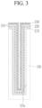
- FIG. 3 is a drawing illustrating region A in FIG. 1 .
- the capacitor 10 may include the structure 100, a first internal electrode 210, a floating electrode 220, a second internal electrode 230, dielectric layers 240, a first external electrode 410, and a second external electrode 420.
- the structure 100 has a first surface 100a and a second surface 100b positioned opposite to each other.
- first surface 100a is positioned on the upper side and the second surface 100b is positioned on the lower side.
- first surface 100a may be referred to as the upper surface
- second surface 100b may be referred to as the lower surface.
- the direction in which the first surface 100a and the second surface 100b are spaced apart from each other may be referred to as a vertical direction.
- the structure 100 may be formed of an insulating material.
- the first surface 100a of the structure 100 has a plurality of openings 101.
- the openings 101 may be columnar spaces recessed from the first surface 100a toward the second surface 100b.
- the structure 100 may be formed of porous anodizing aluminum oxide (AAO), and the openings 101 may be formed by fine pores formed in the anodizing aluminum oxide.
- AAO anodizing aluminum oxide
- the aspect ratios of the fine pores may be in a range from 2000 to 3000.
- the structure 100 may have a structure in which the bottoms of the fine pores are blocked.
- the first internal electrode 210 may be disposed on at least a portion of the region where the openings 101 are positioned.
- the first internal electrode 210 is disposed on the inner surfaces of the openings 101.
- the first internal electrode 210 may be disposed on the sections between adjacent openings 101 on the first surface 100a of the structure 100. Accordingly, the regions of the first internal electrode 210 disposed on the inner surfaces of the openings 101 may be connected to each other by the regions position of the first surface 100a of the structure 100.
- the openings 101 may include first openings 101a, second openings 101b, and third openings 101c.
- first openings 101a one or more are provided as first openings 101a.
- second openings 101b one or more are provided as second openings 101b.
- third openings 101c the remaining openings of the plurality of openings 101, other than the first openings 101a and the second openings 101b, may be provided as third openings 101c.
- the region where the first openings 101a are positioned and the region where the second openings 101b are positioned are spaced apart from each other, and the third openings 101c are positioned between the first openings 101a and the second openings 101b.
- the first external electrode 410 may be disposed in the direction toward which the first surface 100a of the structure 100 faces.
- the first external electrode 410 is disposed on the first internal electrode 210 in the region where the first openings 101a are positioned.
- the first external electrode 410 may face the region where the first openings 101a are positioned, in the vertical direction.
- the first external electrode 410 may be disposed so as to be in contact with the first internal electrode 210 in a region located adjacent to the first openings 101a, thereby being electrically connected to the first internal electrode 210.
- the first external electrode 410 may be a single-layer structure or a multi-layer structure.
- the first external electrode 410 may be disposed on the first internal electrode 210 disposed on a section between first openings 101a.
- the first external electrode 410 may cover one or more first openings 101a. Accordingly, in the first openings 101a positioned below the first external electrode 410, first opening side cavities C1 may be formed on the first internal electrode 210.
- a first opening side insulating layer 310 may be disposed on the portions of the region on the first openings 101a, other than the region where the first external electrode 410 is disposed.
- the first opening side insulating layer 310 may be disposed so as to cover some of the first openings 101a.
- the first opening side insulating layer 310 may cover some of a plurality of first openings 101a. Accordingly, in the first openings 101a positioned below the first opening side insulating layer 310, first opening side cavities C1 may be formed on the first internal electrode 210.
- the material of the first opening side insulating layer 310 may be polyimide or the like.
- a second opening side insulating layer 320 may be disposed on the first internal electrode 210 in the region where the second openings 101b are positioned.
- the second opening side insulating layer 320 may be disposed so as to cover the second openings 101b. Accordingly, in the second openings 101b, second opening side cavities C2 may be formed on the first internal electrode 210.
- the material of the second opening side insulating layer 320 may be polyimide or the like.
- a floating electrode 220 may be disposed on the second opening side insulating layer 320. Accordingly, on the region where the second openings 101b are positioned, the floating electrode 220 may be disposed on the first internal electrode 210 and the second opening side insulating layer 320 may be disposed between the first internal electrode 210 and the floating electrode 220.
- the floating electrode 220 may be disposed on the first internal electrode 210 in the region where the third openings 101c are positioned. In the region where the third openings 101c are positioned, the floating electrode 220 may be formed on the inner regions of the third openings 101c and the sections between the third openings 101c adjacent to each other on the first surface 100a of the structure 100.
- the portion formed on the region where the second openings 101b are positioned may be connected to the portion formed on the region where the third openings 101c are positioned.
- the floating electrode 220 may not be on the first internal electrode 210 in the region where the first openings 101a are positioned. In other words, the floating electrode 220 may not be formed on the first openings 101a and the first internal electrode 210 disposed on the region on the first surface 100a between first openings 101a adjacent to each other.
- the floating electrode 220 may be formed on a plurality of layers.
- the second internal electrode 230 is disposed on the floating electrode 220.
- the second internal electrode 230 may be disposed on the region where the second openings 101b are positioned and the region where the third openings 101c are positioned.
- the second internal electrode 230 may be formed on the inner regions of the third openings 101c and the sections on the second surface 100b of the structure 100 between the third openings 101c adjacent to each other.
- third opening side cavities C3 may be formed on the second internal electrode 230.
- the second internal electrode 230 may be disposed so as to fill the third openings 101c, such that the third openings 101c do not have third opening side cavities C3.
- the second internal electrode 230 is not on the first internal electrode 210 in the region where the first openings 101a are positioned.
- the dielectric layers 240 are disposed only on some portions of the first internal electrode 210.
- the dielectric layers 240 may be disposed only on the regions where the second openings 101b and the third openings 101c are positioned.
- the dielectric layers 240 may be disposed between the first internal electrode 210 and the floating electrode 220. In the region where the second openings 101b are positioned, the dielectric layers 240 may be disposed on the second opening side insulating layer 320. Accordingly, in the region where the second openings 101b are positioned, the dielectric layers 240 may be disposed between the floating electrode 220 and the second opening side insulating layer 320. Further, in the region where the second openings 101b are positioned, the second opening side insulating layer 320 may be disposed between the first internal electrode 210 and the dielectric layers 240. In the region where the third openings 101c are positioned, the dielectric layers 240 may be disposed between the first internal electrode 210 and the floating electrode 220.
- the dielectric layers 240 may be disposed between the layers of the floating electrode 220.
- the dielectric layers 240 are disposed. In the region where the second openings 101b are positioned, a dielectric layer 240 may be disposed between the floating electrode 220 and the second internal electrode 230. In the region where the third openings 101c are positioned, a dielectric layer 240 may be disposed between the floating electrode 220 and the second internal electrode 230.
- the dielectric layers 240 may not be on the first internal electrode 210 in the region where the first openings 101a are positioned. In other words, the dielectric layers 240 may not be formed on the first openings 101a and the first internal electrode 210 disposed in the regions of the first surface 100a between the first openings 101a adjacent to each other.
- the second external electrode 420 may be disposed in the direction toward which the first surface 100a of the structure 100 faces.
- the second external electrode 420 is disposed apart from the first external electrode 410.
- the second external electrode 420 is disposed on the second internal electrode 230.
- the second external electrode 420 may be disposed so as to be in contact with the second internal electrode 230, thereby being electrically connected to the second internal electrode 230.
- the second external electrode 420 may be disposed on the region where the second openings 101b are positioned, so as to face the region where the second openings 101b are positioned, in the vertical direction. Accordingly, below the second external electrode 420, the second opening side insulating layer 320 and the second opening side cavities C2 may be positioned.
- the second external electrode 420 may be a single-layer structure or a multi-layer structure.
- the capacitor 10 In the capacitor 10 according to the embodiment, most of the first internal electrode 210 and the second internal electrode 230 are disposed on the openings 101. For convenience, in FIGS. 1 to 3 , only some of the openings 101 are shown; however, a very large number of openings 101 are positioned as nanostructures in the structure 100 which is anodizing aluminum oxide (AAO). Accordingly, on a plane intersecting the direction in which the first surface 100a and second surface 100b of the structure 100 face each other, the surface area of the first internal electrode 210 and the second internal electrode 230 is very large with respect to the area occupied by the structure 100. As a result, the capacitor 10 according to the embodiment has very high capacity relative to its size.
- AAO aluminum oxide
- the floating electrode 220 is disposed between the first internal electrode 210 and the second internal electrode 230. Specifically, on the regions where the second openings 101b and the third openings 101c are positioned, the floating electrode 220 is disposed between the first internal electrode 210 and the second internal electrode 230. Accordingly, the voltage difference between the first internal electrode 210 and the second internal electrode 230 is distributed by the floating electrode 220. Specifically, the voltage difference between the first internal electrode 210 and the second internal electrode 230 is caused by the voltage difference between the first internal electrode 210 and the floating electrode 220 and the voltage difference between the floating electrode 220 and the second internal electrode 230. Accordingly, in the capacitor 10 according to the embodiment, the magnitude of the breakdown voltage increases and thus the possibility of a breakdown phenomenon occurring significantly decreases.
- the cavities C1 and C2 may be formed inside the openings 101 positioned below the external electrodes 410 and 420. These cavities C1 and C2 may prevent cracks from being caused in the internal electrodes 210 and 230, the dielectric layers 240, and the like by a force (for example, vibration or compression) that is applied to the external electrodes 410 and 420 and under the external electrodes 410 and 420 in the process of mounting the capacitor 10.
- a force for example, vibration or compression
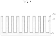
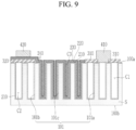
- FIGS. 4 to 9 are drawings illustrating a method of manufacturing the capacitor 10 according to the embodiment.
- a substrate S to form the structure 100 is provided.
- the substrate S is provided with a plurality of openings 101 formed therein.
- the substrate S may be provided so as to have an area capable of accommodating two or more capacitors 10.
- the substrate S may be formed of anodizing aluminum oxide (AAO), and the openings 101 may be fine pores formed by an anodization method. In this case, the openings 101 are provided in a downwardly blocked state.
- the diameters of the openings 101 may be in a range from 50 nm to 300 nm.
- the diameters of the openings 101 may be diameters measured from the upper ends of the openings 101.
- the first internal electrode 210 is formed on the inner surfaces of the openings 101. Also, the first internal electrode 210 is formed on the regions where the openings 101 are adjacent to each other. Accordingly, the first internal electrode 210 is continuously formed.
- the first internal electrode 210 may be formed by a deposition process. Chemical vapor deposition (CVD), atomic layer deposition (ALD), and the like may be used to form the first internal electrode 210.
- the first internal electrode 210 may be formed to a thickness of several nanometers to several tens of nanometers.
- the first internal electrode 210 may be formed of TiN or the like.
- a first insulating layer IL1 is formed on the region where the first openings 101a are positioned, and a second insulating layer IL2 is formed on the region where the second openings 101b are positioned.
- a mask in which regions where the first insulating layer IL1 and the second insulating layer IL2 are to be formed are open may be formed on the structure 100 by a photolithography process. Then, the first insulating layer IL1 and the second insulating layer IL2 may be formed on the structure 100 through the mask.
- the first insulating layer IL1 and the second insulating layer IL2 may be formed by a deposition process. Chemical vapor deposition (CVD), atomic layer deposition (ALD), or the like may be used to form the first insulating layer IL1 and the second insulating layer IL2. Thereafter, the mask may be removed by a strip process.
- CVD chemical vapor deposition
- ALD atomic layer deposition
- a dielectric layer 240, the floating electrode 220, another dielectric layer 240, and the second internal electrode 230 are sequentially formed.
- Each of a dielectric layer 240, the floating electrode 220, another dielectric layer 240, and the second internal electrode 230 is formed simultaneously on the region where the second openings 101b are positioned and the region where the third openings 101c are positioned. Accordingly, in each of a dielectric layer 240, the floating electrode 220, another dielectric layer 240, and the second internal electrode 230 sequentially formed, the portion on the region where the second openings 101b are positioned is connected to the portion on the region where the third openings 101c are positioned.
- a dielectric layer 240, the floating electrode 220, another dielectric layer 240, and the second internal electrode 230 are formed on the second insulating layer IL2. Further, a dielectric layer 240, the floating electrode 220, another dielectric layer 240, and the second internal electrode 230 are formed on the inner surfaces of the third openings 101c and the sections between the third openings 101c adjacent to each other.
- the dielectric layers 240 may be formed by a deposition process. Chemical vapor deposition (CVD), atomic layer deposition (ALD), and the like may be used to form the dielectric layers 240.
- the dielectric layers 240 may be formed of one of metal oxides such as Al 2 O 3 , ZrO 2 , HfO 2 , etc. Alternatively, the dielectric layers 240 may be formed of a combination of metal oxides such as Al 2 O 3 , ZrO 2 , HfO 2 , etc. Also, the dielectric layers 240 may be formed of a ZAZ layer which is a composite layer of a ZrO 2 layer, an Al 2 O 3 layer, and a ZrO 2 layer.
- the thicknesses of each of the ZrO 2 , Al 2 O 3 , and ZrO 2 layers may be in a range from 1.9 nm to 2.1nm, a range from 0.29 nm to 0.31nm, and a range from 1.9 nm to 2.1nm, respectively.
- the floating electrode 220 may be formed by a deposition process. Chemical vapor deposition (CVD), atomic layer deposition (ALD), and the like may be used to form the floating electrode 220.
- the floating electrode 220 may be formed of TiN or the like.
- the second internal electrode 230 may be formed by a deposition process. Chemical vapor deposition (CVD), atomic layer deposition (ALD), and the like may be used to form the second internal electrode 230.
- the second internal electrode 230 may be formed of TiN or the like.
- the second internal electrode 230 may be formed so as not to fully fill the insides of the third openings 101c such that in the third openings 101c, the third opening side cavities C3 are formed on the second internal electrode 230.
- the second internal electrode 230 may be formed so as to fill the third openings 101c, such that the third openings 101c do not have the third opening side cavities C3.
- the dielectric layer 240, the floating electrode 220, another dielectric layer 240, and the second internal electrode 230 are prevented from being deposited on the inner sides of the first openings 101a.
- the first opening side cavities C1 are formed inside the first openings 101a positioned below the first insulating layer IL1.
- the dielectric layer 240, the floating electrode 220, another dielectric layer 240, and the second internal electrode 230 are prevented from being deposited on the inner sides of the second openings 101b.
- the second opening side cavities C2 are formed inside the second openings 101b positioned below the second insulating layer IL2.
- a portion of the first insulating layer IL1 is etched, such that the first opening side insulating layer 310 are formed. Further, from the regions where the first insulating layer IL1 is etched, the first internal electrode 210 is exposed to the outside.
- the process of etching the first insulating layer IL1 may be performed after a mask in which the etch region is open is formed by a photolithography process. Further, the second insulating layer IL2 becomes the second opening side insulating layer 320.
- the first external electrode 410 and the second external electrode 420 are formed.
- the first external electrode 410 may be formed on the first internal electrode 210 exposed to the outside in the region where the first openings 101a are positioned.
- the second external electrode 420 may be formed on the second internal electrode 230.
- the second external electrode 420 may be formed on the region where the second openings 101b are positioned.
- the first external electrode 410 and the second external electrode 420 may have a multi-layer structure by forming seed layers and then forming the other portions on the seed layers.
- the seed layers may be formed of a metal material such as Ti, Cu, etc.
- the seed layers may be formed by a sputtering process.
- the other portions that are formed on the seed layers may be formed by a plating process using Cu, Sn, Ag, etc.
- the substrate S may be diced such that the regions where individual capacitors 10 are positioned are separated from one another.
- the dicing process may be performed with a blade, a laser, or the like.
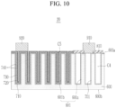
- FIG. 10 is a drawing illustrating a capacitor 20 according to another embodiment.
- the structure 600 has a first surface 600a and a second surface 600b positioned opposite to each other.
- first surface 600a is positioned on the upper side and the second surface 600b is positioned on the lower side.
- first surface 600a may be referred to as the upper surface
- second surface 600b may be referred to as the lower surface.
- the direction in which the first surface 600a and the second surface 600b are spaced apart from each other may be referred to as a vertical direction.
- the structure of the structure 600 is identical or similar to that of the structure 100 of the capacitor 10 according to an embodiment, and thus a redundant description thereof will not be made.
- the openings 601 may include first openings 601a and second openings 601b. Among the plurality of openings 601, one or more are provided as first openings 601a. Further, the remaining openings of the plurality of openings 601 other than the first openings 601a may be provided as second openings 601b.
- the first external electrode 910 may be disposed on the first internal electrode 710 disposed on a section between first openings 601a.
- the first external electrode 910 may cover one or more first openings 601a. Accordingly, in the first openings 601a positioned below the first external electrode 910, first opening side cavities C4 may be formed on the first internal electrode 710. Further, on the portions of the region on the first openings 601a, other than the region where the first external electrode 910 is disposed, a first opening side insulating layer 810 may be disposed.
- the first opening side insulating layer 810 may be disposed so as to cover some of the first openings 601a. Accordingly, in the first openings 601a positioned below the first opening side insulating layer 810, first opening side cavities C4 may be formed on the first internal electrode 710.
- the floating electrode 720 may be disposed on the first internal electrode 710 in the region where the second openings 601b are positioned. In the region where the second openings 601b are positioned, the floating electrode 720 may be formed on the inner regions of the second openings 601b and the sections between the second openings 601b adjacent to each other on the first surface 600a of the structure 600.
- the second internal electrode 730 is not on the first internal electrode 710 in the region where the first openings 601a are positioned.
- the dielectric layers 740 may not be on the first internal electrode 710 in the region where the first openings 601a are positioned. In other words, the dielectric layers 740 may not be formed on the first openings 601a and the first internal electrode 710 disposed in the regions of the first surface 600a between the first openings 601a adjacent to each other.
- the second external electrode 920 may be disposed on the first surface (600a) side of the structure 600.
- the second external electrode 920 is disposed on the second internal electrode 730.
- the second external electrode 920 may be disposed so as to be in contact with the second internal electrode 730, thereby being electrically connected to the second internal electrode 730.
- the second external electrode 920 may be disposed on the region where the second openings 601b are positioned, so as to face the region where the second openings 601b are positioned, in the vertical direction.
- the second external electrode 920 may be a single-layer structure or a multi-layer structure.
Landscapes
- Engineering & Computer Science (AREA)
- Power Engineering (AREA)
- Microelectronics & Electronic Packaging (AREA)
- Manufacturing & Machinery (AREA)
- Chemical & Material Sciences (AREA)
- Inorganic Chemistry (AREA)
- Fixed Capacitors And Capacitor Manufacturing Machines (AREA)
- Ceramic Capacitors (AREA)
Applications Claiming Priority (1)
| Application Number | Priority Date | Filing Date | Title |
|---|---|---|---|
| KR1020230188405A KR20250097288A (ko) | 2023-12-21 | 2023-12-21 | 커패시터 |
Publications (2)
| Publication Number | Publication Date |
|---|---|
| EP4576142A2 true EP4576142A2 (de) | 2025-06-25 |
| EP4576142A3 EP4576142A3 (de) | 2025-08-06 |
Family
ID=91959280
Family Applications (1)
| Application Number | Title | Priority Date | Filing Date |
|---|---|---|---|
| EP24189478.1A Pending EP4576142A3 (de) | 2023-12-21 | 2024-07-18 | Kondensator |
Country Status (4)
| Country | Link |
|---|---|
| US (1) | US20250210256A1 (de) |
| EP (1) | EP4576142A3 (de) |
| JP (1) | JP2025100318A (de) |
| KR (1) | KR20250097288A (de) |
Citations (1)
| Publication number | Priority date | Publication date | Assignee | Title |
|---|---|---|---|---|
| US20170278636A1 (en) * | 2014-12-08 | 2017-09-28 | Eestor, Inc. | Enhanced stacking for improved capacitance |
Family Cites Families (4)
| Publication number | Priority date | Publication date | Assignee | Title |
|---|---|---|---|---|
| US8085524B2 (en) * | 2005-11-08 | 2011-12-27 | Ipdia | Integrated capacitor arrangement for ultrahigh capacitance values |
| US20090141426A1 (en) * | 2007-11-29 | 2009-06-04 | Cheol-Seong Hwang | Thin film multi-layered ceramic capacitor and method of fabricating the same |
| KR102122935B1 (ko) * | 2013-03-29 | 2020-06-26 | 삼성전기주식회사 | 적층 세라믹 커패시터 및 그 제조 방법 |
| US10867752B2 (en) * | 2017-09-28 | 2020-12-15 | Samsung Electro-Mechanics Co., Ltd. | Capacitor and method of manufacturing the same |
-
2023
- 2023-12-21 KR KR1020230188405A patent/KR20250097288A/ko active Pending
-
2024
- 2024-07-10 US US18/768,880 patent/US20250210256A1/en active Pending
- 2024-07-18 EP EP24189478.1A patent/EP4576142A3/de active Pending
- 2024-08-20 JP JP2024139007A patent/JP2025100318A/ja active Pending
Patent Citations (1)
| Publication number | Priority date | Publication date | Assignee | Title |
|---|---|---|---|---|
| US20170278636A1 (en) * | 2014-12-08 | 2017-09-28 | Eestor, Inc. | Enhanced stacking for improved capacitance |
Also Published As
| Publication number | Publication date |
|---|---|
| EP4576142A3 (de) | 2025-08-06 |
| JP2025100318A (ja) | 2025-07-03 |
| KR20250097288A (ko) | 2025-06-30 |
| US20250210256A1 (en) | 2025-06-26 |
Similar Documents
| Publication | Publication Date | Title |
|---|---|---|
| CN109585163B (zh) | 电容器及其制造方法 | |
| CN108807669B (zh) | 电容器和具有该电容器的板 | |
| US10403434B2 (en) | Capacitor component | |
| KR20180023657A (ko) | 박막 커패시터 및 그 제조방법 | |
| EP4510189A1 (de) | Kondensator und verfahren zu seiner herstellung | |
| US20250210256A1 (en) | Capacitor | |
| JP2022066346A (ja) | キャパシター及び実装基板 | |
| US20210027951A1 (en) | Capacitor cluster | |
| US20250210276A1 (en) | Capacitor, manufacturing method thereof, and capacitor assembly using the same | |
| EP4510157A2 (de) | Kondensator und verfahren zu seiner herstellung | |
| US10950389B2 (en) | Thin-film capacitor | |
| US10319526B2 (en) | Thin-film capacitor | |
| US20250149242A1 (en) | Multilayer ceramic capacitor | |
| KR20220111141A (ko) | 커패시터, 그 제조방법 및 커패시터용 전극 | |
| US20250210269A1 (en) | Capacitor | |
| US12597560B2 (en) | Capacitor component | |
| US11901125B2 (en) | Capacitor component including unit device having polygonal-shaped cross-section | |
| US20250218680A1 (en) | Capacitor | |
| US20250140476A1 (en) | Capacitor and manufacturing method thereof | |
| US20240071691A1 (en) | Semiconductor device | |
| CN116266500A (zh) | 电容器组件 | |
| KR101853196B1 (ko) | 박막 커패시터 | |
| KR20250098801A (ko) | 캐패시터 | |
| KR20250128648A (ko) | 캐패시터 | |
| KR20250036481A (ko) | 캐패시터 |
Legal Events
| Date | Code | Title | Description |
|---|---|---|---|
| PUAI | Public reference made under article 153(3) epc to a published international application that has entered the european phase |
Free format text: ORIGINAL CODE: 0009012 |
|
| STAA | Information on the status of an ep patent application or granted ep patent |
Free format text: STATUS: THE APPLICATION HAS BEEN PUBLISHED |
|
| AK | Designated contracting states |
Kind code of ref document: A2 Designated state(s): AL AT BE BG CH CY CZ DE DK EE ES FI FR GB GR HR HU IE IS IT LI LT LU LV MC ME MK MT NL NO PL PT RO RS SE SI SK SM TR |
|
| PUAL | Search report despatched |
Free format text: ORIGINAL CODE: 0009013 |
|
| AK | Designated contracting states |
Kind code of ref document: A3 Designated state(s): AL AT BE BG CH CY CZ DE DK EE ES FI FR GB GR HR HU IE IS IT LI LT LU LV MC ME MK MT NL NO PL PT RO RS SE SI SK SM TR |
|
| RIC1 | Information provided on ipc code assigned before grant |
Ipc: H01G 4/33 20060101AFI20250627BHEP Ipc: H01G 4/38 20060101ALI20250627BHEP Ipc: H01G 4/005 20060101ALI20250627BHEP Ipc: H01G 4/012 20060101ALI20250627BHEP Ipc: H01G 4/252 20060101ALI20250627BHEP Ipc: H01G 4/228 20060101ALN20250627BHEP Ipc: H10D 1/68 20250101ALN20250627BHEP |
|
| STAA | Information on the status of an ep patent application or granted ep patent |
Free format text: STATUS: REQUEST FOR EXAMINATION WAS MADE |
|
| 17P | Request for examination filed |
Effective date: 20251031 |
|
| STAA | Information on the status of an ep patent application or granted ep patent |
Free format text: STATUS: EXAMINATION IS IN PROGRESS |