EP4576084A1 - System und verfahren zum chipbonden mit strahlungsfreisetzung - Google Patents
System und verfahren zum chipbonden mit strahlungsfreisetzung Download PDFInfo
- Publication number
- EP4576084A1 EP4576084A1 EP23220056.8A EP23220056A EP4576084A1 EP 4576084 A1 EP4576084 A1 EP 4576084A1 EP 23220056 A EP23220056 A EP 23220056A EP 4576084 A1 EP4576084 A1 EP 4576084A1
- Authority
- EP
- European Patent Office
- Prior art keywords
- die
- donor
- target
- substrate
- radiation
- Prior art date
- Legal status (The legal status is an assumption and is not a legal conclusion. Google has not performed a legal analysis and makes no representation as to the accuracy of the status listed.)
- Pending
Links
Images


Classifications
-
- G—PHYSICS
- G11—INFORMATION STORAGE
- G11C—STATIC STORES
- G11C5/00—Details of stores covered by group G11C11/00
- G11C5/02—Disposition of storage elements, e.g. in the form of a matrix array
- G11C5/04—Supports for storage elements, e.g. memory modules; Mounting or fixing of storage elements on such supports
-
- H10P72/74—
-
- H10W72/0711—
-
- H10W90/00—
-
- H10W99/00—
-
- H10P72/7414—
-
- H10P72/7428—
-
- H10P72/7432—
-
- H10P72/744—
Definitions
- the present disclosure relates generally to a method and tool for die bonding.
- multiple finished or unfinished ICs may be placed in contact, stacked, bonded, or otherwise joined (e.g., to heterogeneous or homogeneous devices) at various points in the fabrication process.
- Heterogeneous integration e.g., the integration of different circuits or other patterned devices, may rely upon joining of specific portions (for example, conductive contact elements) of multiple die-where these specific portions may be aligned in three-dimensional space to ensure functional connectivity.
- Alignment of these die which may have multiple fabrication layers, different critical dimensions, different nodes, packaging, etc., with each other may require different techniques than used for lithography during fabrication.
- improvements in die placement and alignment e.g., improvements in heterogeneous integration
- improvements in IC manufacturing and integration abilities lead to improvements in IC manufacturing and integration abilities.
- a method comprising:
- a method comprising:
- a system comprising:
- a system comprising:
- a system configured to transfer a semiconductor die to an acceptor location in a die bonding process using radiation induced forward transfer and using intermolecular bonding between the die and the acceptor location.
- a system configured to bend a semiconductor die on a carrier structure to allow for contact between part of the die and acceptor location before the die is fully released from the carrier structure.
- one or more non-transitory, machine-readable medium having instructions thereon, the instructions when executed by a processor being configured to perform a method as described herein.
- Embodiments described as being implemented in software should not be limited thereto, but can include embodiments implemented in hardware, or combinations of software and hardware, and vice-versa, as will be apparent to those skilled in the art, unless otherwise specified herein.
- an embodiment showing a singular component should not be considered limiting; rather, the disclosure is intended to encompass other embodiments including a plurality of the same component, and vice-versa, unless explicitly stated otherwise herein.
- the present disclosure encompasses present and future known equivalents to the known components referred to herein by way of illustration.
- wafer may be used generally to refer to a large unit of manufacture (which may be the largest unit of manufacture), while the term “die” may be used to refer to a smaller unit of manufacture which may correspond to a lithography pattern, a portion of a lithography pattern, multiple lithography patterns, etc.
- a “die” may correspond to a portion of "wafer”-that is a “die” may be produced by dicing or otherwise dividing a "wafer”.
- the term “die” should be considered as interchangeable with the term chip, chiplet, or other terms for IC divisions.
- a patterning device (for example, a lithography device) can comprise, or can form, one or more patterns, which may correspond to one or more die.
- the patterns can be generated utilizing CAD (computer-aided design) programs, based on a pattern or design layout, this process often being referred to as EDA (electronic design automation).
- EDA electronic design automation
- All may exclude items, such as excess items. Corresponding may not require that items correspond in an exactly one to one manner. For example, a first item may correspond to two of a second item or vice versa. In some cases, individual may refer to multiple of an item, such as each item A has individual item B, where an item A may have two of an item B.
- FIGS. 1A-1D are schematic diagrams illustrating an exemplary die bonding method consistent with embodiments of the present disclosure.
- the exemplary die bonding method is depicted in relation to a reference set of axes, which are consistent through the schematic illustrations.
- the reference axes are provided for ease of description only and are not to be taken as limiting. Included methods and apparatuses may instead be described with reference to a different set of axes (e.g., cylindrical coordinates, polar coordinates, etc.), a different origin point (e.g., an origin point in the donor die, an origin point in the target, origin point in between the donor die and target, etc.), or a different orientation.
- the reference set of axes is chosen such that the fabrication plane of the die (i.e., a substrate surface) lies in the x-y plane and where the fabrication direction is parallel or antiparallel to the z-axis for both the donor die and target locations.
- the exemplary die bonding method may involve a donor die 102 and a target die 104.
- the term “donor” and the term “target” are used for ease of description. It should be understood that the term “donor” and the term “target” are provided for reference and are relative descriptions, and that elements described as corresponding to a “donor” can instead correspond to a “target” and vice versa.
- a target die may also or instead be called an acceptor die.
- donor die and target die are depicted in Figure 1A , it will be appreciated that there may be multiple such die and that multiple donor die may be essentially simultaneously bonded with multiple target die, e.g., where, for example, multiple die are still part of (all or part) a substrate in or on which they are formed.
- the donor die 102 may have one or more electrically active areas 106, such as on an alignment face of the donor die 102.
- the one or more electrically active areas 106 may be conductive, such as metal.
- the one or more electrically active areas 106 may correspond to one or more vias (e.g., one or more through silicon vias (TSVs)), one or more electrical contact lines, one or more contact pads, one or more packaging pads, or other one or more electrically conductive areas.
- TSVs through silicon vias
- the donor die 102 may have one or more electrically inert areas (for example, an electrically insulating area) outside of the one or more electrically active areas 106, such as on the alignment face of the donor die 102.
- the one or more electrically active areas 106 may be recessed (as shown) with respect to one or more other surfaces of the donor die 102.
- the one or more electrically active areas 106 may correspond to one or more contacts (e.g., to source, to drain, to gate, etc.) to one or more electrical devices within the donor die 102 (not shown).
- the target die 104 likewise, may have one or more electrically active areas 108, which may have one or more similar properties to the one or more electrically active areas 106.
- the donor die 102 may also or instead have one or more doped areas 110, such as on an alignment face of the donor die 102, recessed below the alignment face of the donor die 102, etc. While the term "doped" is used, it should be understood that the one or more doped areas 110 may be any areas which, through the course of fabrication, come to have one or more different electrical characteristics than the bulk of the substrate (e.g., silicon wafer).
- the one or more doped areas 110 may correspond to source, drain, gate, ground, or other areas of a circuit which is doped or otherwise altered (e.g., through implantation, oxide growth, thin film deposition, etc.) to have a different electrical characteristic than the bulk of the substrate.
- the one or more doped areas 110 may include one or more conductive layers (e.g., one or more highly doped or electrically conductive layers) and/or one or more insulative layers (e.g., one or more oxide layers).
- the donor die 102 may have one or more undoped areas (for example, an area where the substrate retains the characteristic of the bulk substrate) outside of the one or more doped areas 110, such as on the alignment face of the donor die 102.
- the one or more doped areas 110 may be recessed, buried, coplanar (as shown), etc. with respect to one or more other surfaces of the donor die 102.
- the one or more doped areas 110 may correspond to one or more regions (e.g., to one or more source regions, one or more drain regions, one or more gate regions, one or more dielectric regions, etc.) of one or more electrical devices within the donor die 102 or one or more regions which may form one or more electrical devices across both the donor die 102 and the acceptor die 104 once those die are bonded.
- the target die 104 may have one or more doped areas 112, which may have one or more similar properties to the one or more doped areas 110.
- the exemplary die bonding method may involve alignment of at least one of the electrically active areas 106 and/or doped areas 110 of the donor die 102 with at least one of the electrically active areas 108 and/or doped areas 112 of the target die 104.
- the exemplary die bonding method may involve bringing the donor die 102 into contact with the target die 104 while maintaining alignment between, e.g., one or more electrically active areas 106 and one or more electrically active areas 108 so that the one or more electrically active areas 106 and the one or more electrically active areas 108 may be joined for cross-die electrical communication.
- the exemplary die bonding method may involve aligning one or more doped areas 110 of the donor die 102 with one or more doped areas 112 of the target die 104. Aligning may encompass bringing into contact, aligning one or more edges of various regions, having overlap, having non-overlap, or any other appropriate alignment scheme.
- the exemplary die bonding method may involve applying or maintaining pressure between the donor die 102 and the target die 104, while bonding occurs between the donor die 102 and the target die 104.
- the donor die 102 may be supported by a carrier structure 114, which may be a substrate which is transparent to a range of radiation (e.g., infrared radiation, a portion of the optical spectrum, etc.).
- the target die 104 may likewise be supported by a carrier structure 116, which may or may not be transparent to a range of radiation.
- the target die 104 (possibly together with the carrier structure) may be part of an undiced or partially diced target wafer.
- the alignment may be complicated by the multiple layers of the donor die 102 or the multiple layers of the target die 104, which may be optically opaque.
- Figures 1A and 1B depict a cross-sectional view of portions of the exemplary die bonding method showing relative positioning between the donor die 102 and the target die 104.
- the donor die 102 and the target die 104 may be brought together along the z-axis, while the position of the donor die 102 or the target die 104 may be adjusted in the x-y plane (e.g., perpendicular to the z-axis of approach), such as to improve alignment between the donor die 102 and the target die 104.
- alignment can be achieved between, e.g., one or more electrically active areas 106 and one or more electrically active areas 108 and/or between one or more doped areas 110 of the donor die 102 with one or more doped areas 112 of the target die 104.
- the bonding is a direct or fusion bonding (e.g., involving van der Waals forces).
- the bonding is an intermolecular bonding, e.g., van der Waals bonding.
- the bonding may include covalent, ionic, or metallic (e.g., chemical) bonding, e.g., hydrogen bonding.
- the bonding is aided by a material (e.g., a suitable bonding or adhesive material) applied to an alignment surface of the donor die 102 and/or target die 104 or provided to a gap between the donor die 102 and the target die 104 (e.g., in the form of gas or liquid).
- a material e.g., a suitable bonding or adhesive material
- physical contact between the donor die 102 and the target die 104 may include bonding, such as through a bonding wavefront generated by contact (or atomic level proximity), such as of a surface prepared for hydrogen bonding.
- the donor die 102 and the target die 104 may be annealed after contact as depicted by the wavy lines (while wavy lines are shown here at both the donor die 102 and the target die 104, the annealing agent need not be provided at both the donor die 102 and the target die 102 nor needs to be applied in the direction(s) shown).
- Annealing may be or include heat annealing, electrical annealing, electrostatic processes, etc.
- annealing may include annealing of in-plane (or prominent) regions that are bonded and/or annealing of one or more recessed areas which may increase the volume of fill in a recess area (such as through thermal expansion, capillary force, etc.) and may cause physical contact and bonding of areas previously not in contact.
- annealing may cause physical or chemical changes, such as in the one or more electrically active areas 106 of the donor die 102 or in the one or more electrically active areas 108 of the target die 104, which may cause or improve physical contact or electrical contact between an electrically active area 106 and an electrically active area 108.
- Annealing may therefore produce or enhance electrical connectivity between elements of the donor die 102 and the target die 104 (e.g., integration). This electrical connectivity may occur even if an electrically active area 106 and an electrically active area 108 differ-for example, have different recessed depths, are made up of different materials, have different dimensions, etc.
- the prior bonding described with respect to Figure 1A may be temporary during one or more portions of the annealing process, wherein the annealing process forms tight connections between donor die 102 and the target die 104.
- the annealing may occur in the system where the bonding occurs.
- the annealing may occur in a separate system from the system in which the bonding occurs, e.g., the donor and target dies are transported out of the bonding system into an annealing system which can include one or more heating elements (e.g., one or more electrical heating elements, one or more elements to provide radiation heating, etc.) to provide the heat for the annealing.
- the heating elements e.g., one or more electrical heating elements, one or more elements to provide radiation heating, etc.
- the carrier structure 114 may be removed as shown in Figure 1B . Additionally or alternatively, the carrier structure 116 may be removed then as well. Alternatively, once the donor die 102 and the target die 104 are annealed, the carrier structure 116 may be removed as shown in Figure 1C . Additionally or alternatively, the carrier structure 114 may be removed then as well.
- Figure 1D depicts a plan view of an example die bonding method according to this disclosure.
- the donor die 102 and the target die 104 may have one or more alignment marks along the x-y plane to facilitate alignment of the die as a whole.
- Alignment marks in the x-y plane of a die e.g., one or more alignment marks 120 on the donor die 102 or one or more alignment marks 122 on the target die 104 may reduce the area available for circuitry.
- One or more alignment marks may be placed in a waste area, such as an area between chips, which may then be destroyed (e.g., removed) during dicing.
- Dicing herein refers to mechanical separation of areas of a substrate (e.g., a unit of manufacture) into smaller areas (e.g., dies or chips) which may contain one or more units of operation (e.g., a logic device, a memory unit, etc.). Dicing may operate using any appropriate method-for example, scribing and breaking, mechanical sawing, laser cutting, etc.-and may destroy (e.g., grind to powder or otherwise render inoperable for circuitry placement) a non-zero linewidth portion of the substrate volume when separating die. Alignment marks may be additively or substractively fabricated, such as by etching or deposition in the z-direction. Alignment marks 120 and 122 may be the same or different.
- Alignment marks 120 and 122 may be a multi-directional alignment mark, i.e., capable of determining alignment in more than one direction, such as a bi-direction alignment mark, an example of which is shown as mark 120 in Figure 1D .
- the alignment mark 120 and/or alignment mark 122 may be a fine alignment mark, such as for alignment in the ⁇ m scale.
- the alignment mark 120 may be located on the donor die 102 while the target die 104 may have an alignment mark 122 located in a waste area, or vice versa.
- one or more electrically active and/or doped areas of the donor die 102 or one or more electrically active and/or doped areas of the target die 104 (not shown in Figure 1D ) or other surface features may function as a reference for alignment (e.g., an alignment mark) of the donor die 102 and/or the target die 104.
- the donor die 102 and the target die 104 may be aligned in up to three dimensions before or during contact between the donor die 102 and the target die 104.
- the donor die 102 or the target die 104 may be positioned in the x-y plane as the donor die 102 in the target die 104 are contacted.
- the donor die 102 or the target die 104 may be positioned by operation of a die actuator or other die-scale elements, such as by piezoelectric stepper elements, or by operation of a chuck or other carrier structure-scale elements, such as by a motor or other actuator.
- the position of the donor die 102 or the target die 104 may be adjusted with respect to up to six degrees of freedom.
- the donor die 102 may be positioned by movement along the X axis (e.g., in a positive or negative X direction), along the y-axis (e.g. in a positive or negative Y direction), along the z-axis (e.g., in a positive or negative Z direction).
- the donor die 102 may also be positioned rotationally with respect to each of those axes-e.g., rotated with respect to the x-axis, rotated with respect to the y-axis, rotated with respect to the z-axis.
- the donor die 102 may be positioned by free movement in space accounted for by six different types of movement (where the movements listed above are provided as examples but where the movements may be described by other axes).
- the target die 104 may be positioned alone or combined with positioning of the donor die 102. Positioning or adjustment of position herein, unless the context otherwise requires, includes displacement, rotation or any combination thereof.
- one or more alignment mark may be rendered invisible (such as due to opacity of a die) to an alignment measurement tool.
- the alignment of the flipped die may therefore be performed based on previously measured positions of the die (e.g., of the one or more alignment marks of the die) with respect to a structure, such as the donor die 102 with respect to the carrier structure 114 or such as the target die 104 with respect to the carrier structure 116.
- Figures 2A-2F are schematic diagrams illustrating an example method of die placement.
- Figures 2A-2F are described with reference to "donor die” (and “donor substrate” containing multiple “donor die”) and “target die” (and “target substrate” containing multiple “target die”), which are relative descriptors and donor die may instead be target die and vice versa.
- Figures 2A-2F are described with respect to donor die and target die, but may instead be a donor substrate or target substrate, where a "substrate” may contain multiple "die”, including un-diced (e.g., unseparated) die in the form of all or part of a semiconductor wafer.
- Figure 2A-2F are cross-sectional views of die placement of donor dies (e.g., donor die 202A, 202B, 202C) on target dies (e.g., target die 204A and target die 204B).
- donor dies e.g., donor die 202A, 202B, 202C
- target dies e.g., target die 204A and target die 204B.
- multiple steps which are depicted as occurring substantially simultaneously in Figures 2A-2F may be performed sequentially.
- multiple steps which are depicted as occurring sequentially in Figures 2A-2F may be performed substantially simultaneously.
- multiple donor dies may be aligned or placed on their respective target dies substantially simultaneously, including donor dies which are proximate (including adjacent) or distant (e.g., non-adjacent but within the same target substrate).
- steps may be performed in a different order.
- Figure 2A is a cross-sectional view of donor dies 202A-202C which are to be placed on target dies 204A-204B.
- the donor dies 202A-202C are supported by a carrier structure 214.
- the donor dies 202A-202C may be adhered to the carrier structure 214 in any appropriate manner, such as by vacuum adhesion, electrostatic adhesion, intermolecular adhesion, van der Waals adhesion, mechanical interlocking, surface reaction, static friction, gravitational force, etc.
- the donor dies 202A-202C may be adhered to the carrier structure 214 by use of, for example, an adhesive (e.g., glue), such as an organic, polymer glue.
- an adhesive e.g., glue
- the carrier structure 214 may be a transparent substrate, such as glass, sapphire, polymer, etc. substrate.
- the donor dies 202A-202C may be placed on the carrier structure 214 by any appropriate method, such as by a pick and place tool.
- the carrier structure 214 may be supported by a chuck or any other appropriate support structure.
- the target dies 204A-204B are supported by a support structure 216.
- the target dies 204A-204B may be part of an undiced or partially diced target wafer.
- the target dies 204A-204B may be adhered to the support structure 216 in any appropriate manner, such as by vacuum adhesion, electrostatic adhesion, intermolecular adhesion, mechanical interlocking, surface reaction, static friction, gravitational force, etc.
- the target dies 204A-204B may be adhered to the support structure 216 by use of, for example, an adhesive (e.g., glue), such as an organic, polymer glue.
- an adhesive e.g., glue
- the support structure may be a carrier structure (e.g., like carrier structure 214) and may be a transparent substrate, such as glass, sapphire, polymer, etc. substrate.
- the target dies 204A-204B may be placed on the support structure 216 by any appropriate method, such as by a pick and place tool.
- the support structure 216 may be, or may be supported by, a chuck or any other appropriate structure.
- the donor dies 202A-202C and the target dies 204A-204B may be aligned with one another at alignment points 203A and 205A (for donor die 202A and target die 204A), alignment points 203B and 205B (for donor die 202B and target die 204B), and alignment points 203C and 205C (for donor die 202C and target die 204B).
- multiple donor die may be placed on a single target die, and vice versa, such as depending on integration goals.
- the alignment points 203A-203C are depicted for the donor dies 202A-202C, while the alignment points 205A-205C are depicted for the target dies 204A-204B.
- the alignment points may be alignment marks (for example, the alignment marks of Figure 1D ), die edges, die corners, other features on edges or surfaces of die.
- the alignment points may be used to align donor and target die, such as by measurement of the locations of various alignment points and then adjustment of the position of the donor and/or target die, such as by movement of a carrier structure supporting the die, to align an alignment point of the donor die with an alignment point of the target die (or vice versa).
- the alignment points may be aligned directly to one another (e.g., as depicted in Figures 2A-2F ). In some embodiments, the alignment points may be aligned relative to one another (e.g., in a predetermined relationship, such as separated by a vector), such as depicted in the bottom of Figure 1D , where the alignment marks are non-overlapping.
- the carrier structure 214 (and/or the structure 216) may be positioned, such as in the X-Y plane, in order to align the alignment point 203A of the donor die 202A with the alignment point 205A of the target die 204A.
- the donor die 202A may be released from the carrier structure 214 by any appropriate mechanism, such as release mechanism 230A.
- the donor die 202A meets the target die 204A at alignment point 207A.
- the release of the donor die 202A may be facilitated by gravity, by electrostatic forces, by physical forces, etc.
- the alignment of the donor die 202A and the target die 204A at the alignment point 207A (which represents a combination of the alignment point 203A and the alignment point 205A of Figure 2A ) may be assisted by any appropriate alignment mechanism, including self-alignment (e.g., attraction of one area of the donor die 202A to a corresponding area of the target die 204A).
- the release occurs while donor die 202A is in (at least partial) contact with target die 204A.
- the release occurs before donor die 202A is in contact with the target die 204A.
- the carrier structure 214 and alternately or additionally the structure 216 may be moved to bring another donor die (e.g., the donor die 202C) into alignment with another target die (e.g., the target die 204B).
- the alignment of alignment point 203C (of donor die 202C) and alignment point 205C (of target die 204B) may be based on measurements of the relative positions of the alignment points (such as using an alignment mark or feature on a die or carrier structure, using a position of an alignment point on another donor or target die, etc.).
- the alignment of alignment point 203C (of donor die 202C) and alignment point 205C (of target die 204B) may be based on one or more substantially simultaneous measurement of the relative positions of an alignment point, such as using an alignment mark or feature of a die or carrier structure, using an alignment target or feature of another donor or target die, etc.
- alignment of only one donor die (e.g., the donor die 202C) and target die (e.g., the target die 204B) is depicted, alignment of one or more sets of donor and target dies may occur substantially simultaneously, such as if for a given relative position of the carrier structure 214 and the support structure 216 the alignment points of multiple donor dies are aligned with the alignment points of multiple target dies.
- the ability to place multiple donor dies substantially simultaneously may depend on the placement of the donor dies on the carrier structure 214 and the ability of the release mechanism to release multiple donor dies.
- the donor die 202C may be released from the carrier structure 214 by any appropriate mechanism, such as release mechanism 230C.
- the donor die 202C meets the target die 204B at alignment point 207C.
- the release of the donor die 202C may be facilitated by gravity, by electrostatic forces, by physical forces, etc.
- the alignment of the donor die 202C and the target die 204B at the alignment point 207C (which represents a combination of the alignment point 203C and the alignment point 205C of Figure 2A ) may be assisted by any appropriate alignment mechanism, including self-alignment.
- the release occurs while donor die 202B is in (at least partial) contact with target die 204B.
- the release occurs before donor die 202B is in contact with the target die 204B.
- the carrier structure 214 and alternately or additionally the structure 216 may be moved to bring another donor die (e.g., the donor die 202B) into alignment with another target die (e.g., the target die 204B).
- the alignment of alignment point 203B (of donor die 202B) and alignment point 205B (of target die 204B) may be based on previous measurements of the relative positions of the alignment points (such as using an alignment mark on a die or carrier structure, using an alignment point on another donor or target die, etc.).
- the alignment of alignment point 203B (of donor die 202B) and alignment point 205B (of target die 204B) may be based on one or more substantially simultaneous measurement of the relative positions of an alignment point, such as using an alignment mark or feature of a die or carrier structure, using an alignment target or feature of another donor or target die, etc.
- the donor die 202B and the donor die 202C are aligned to the same target die (e.g., the target die 204B).
- the donor die are placed on the target die in a substantially one-to-one relationship (e.g., as depicted for the donor die 202A and the target die 204A).
- multiple donor die may be placed on the same target die (or donor die).
- multiple donor die may be placed on un-diced (e.g., unseparated) target die (or donor die), such as all or part of a substrate containing target die (or donor die).
- a donor die may be placed on a target die that has multiple die, including stacked (e.g., bonded) die, such as in a three layer die bonding stack.
- the donor die 202B may be released from the carrier structure 214 by any appropriate mechanism, such as release mechanism 230B.
- the donor die 202B meets the target die 204B at alignment point 207B.
- the release of the donor die 202B may be facilitated by gravity, by electrostatic forces, by physical forces, etc.
- the alignment of the donor die 202B and the target die 204B at the alignment point 207B (which represents a combination of the alignment point 203B and the alignment point 205B of Figure 2A ) may be assisted by any appropriate alignment mechanism, including self-alignment.
- the release occurs while donor die 202B is in (at least partial) contact with target die 204B.
- the release occurs before donor die 202B is in contact with the target die 204B.
- Figures 3A-3J are schematic diagrams illustrating portions of an example apparatus for die bonding.
- Figures 3A-3J are described with reference to "donor die” and "target die", which are relative descriptors as used herein and donor die may instead be target die and vice versa.
- Each of Figures 3A , 3C , 3E , 3G , and 3I is a plane view of an apparatus during placement of donor die on the target die.
- Figures 3B , 3D , 3F , 3H , and 3J is a cross-sectional view of the apparatus during placement of donor die on the target die.
- a donor substrate 300 and a target substrate 350 are depicted as circular, but may instead be any appropriate shape, including rectangular, square, etc.
- the donor substrate 300 (and target substrate 350) may be the substrate in or on which the donor die (target die) have been formed.
- the donor substrate 300 (target substrate 350) may be a "reconstructed wafer", in which donor die (target die) (or other disparate portions of a semiconductor substrate) are arranged or supported on a carrier structure, e.g., to be in position suitable for die bonding.
- the donor substrate 300 may be a carrier structure and donor die (target die), where the donor die (target die) may be held (e.g., adhered) to the carrier structure by any appropriate method, such as by gravitational force, by adhesive (e.g., organic, polymer adhesive), by electrostatic forces, etc.
- the donor substrate 300 (target substrate 350) may contain previously tested donor die (target die), such as donor die (target die) that passed a failure analysis or other post fabrication testing.
- the donor substrate 300 (target substrate 350) may contain donor die (target die) from the same or different semiconductor substrates (e.g., fabrication substrates), including donor die (target die) of different types, different dimensions, etc.
- the donor substrate 300 may have donor die (target die) placed on the donor substrate 300 (target substrate 350) by any appropriate method, such as a pick and place tool.
- the donor substrate 300 (target substrate 350) may be supported, such as by a carrier structure, vacuum chuck, electrostatic chuck, etc., by either a top side (e.g., fabrication face) or backside (e.g., bulk substrate or carrier structure face) or by different faces at various points.
- the donor substrate 300 or donor die (target substrate 350 or target die) may have fabricated devices on multiple faces, such as through silicon vias (TSVs), contact pads, etc., such that both a top side and backside are fabrication faces.
- TSVs through silicon vias
- the donor substrate 300 may be placed on a substrate chuck 320A.
- the substrate chuck 320A may be an appropriate substrate chuck, such as to support the donor substrate 300 in the form of a semiconductor substrate or a carrier structure of the donor substrate 300.
- the substrate chuck 320A may be supported by a support structure 322A.
- the support structure 322A may be a moveable support structure, which may move in the X-Y plane, such as from a first position where the substrate chuck 320A receives the donor substrate 300 to a second position where the donor substrate 300 may be subjected to metrology.
- the substrate chuck 320A may contain (e.g., support) one or more die actuators or other mechanical or electrical actuators which may move a donor die or the donor substrate 300 in one or more dimension, including in the X-Y plane, in the Z-direction, rotationally, etc.
- the substrate chuck 320A may have one or more alignment marks, such as to allow a camera or other measurement system to track the position of the substrate chuck 320A.
- the substrate chuck 320A may have multiple sets of alignment marks, such as coarse alignment marks and/or fine alignment marks.
- the substrate chuck 320A may move, such as by action of the support structure 322A, from one position to another, in free space, etc.
- the support structure 322A may be configured to move in multiple directions and in multiple scales (e.g., in a coarse step and a fine step), such as by multiple motors or steppers.
- the support structure 322A may be activated by a controller of the example apparatus-where the controller of the example apparatus (not depicted) may also control the placement of the donor substrate 300 on the substrate chuck 320A and other operations described herein.
- the substrate chuck 320A may have a measurement point (or alignment point), such as identified by a cruciform measurement mark 327 and a round zero measurement mark 328, which are provided merely as examples and where any appropriate zero measurement mark may be used.
- the measurement point may be used to place the donor substrate 300 on the substrate chuck 320A, such as during movement of the substrate onto the chuck (for example, by insertion of the donor substrate by a substrate handler).
- the measurement point may be used to measure relative positions of the donor die of the donor substrate 300 once the donor substrate 300 is placed on the substrate chuck 320A.
- the placement of the donor die may be measured, such as with up to nm precision, with respect to the measurement point.
- the measurement of the position of the donor die after their placement may be obtained from any appropriate measurement system, such as optical microscopy, reflectometry, etc.
- Figure 3A also depicts a further substrate chuck 320B on a support structure 322B.
- the substrate chuck 320B may be any appropriate substrate chuck, such as substantially identical to the substrate chuck 320A.
- the support structure 322B may be any appropriate support structure, such as substantially identical to the support structure 322A.
- the substrate chuck 320B and the substrate chuck 320A may be substantially indistinguishable.
- the support structure 322B and the support structure 322A may be substantially indistinguishable.
- two substrate chucks and two support structures are depicted, in some embodiments more or less substrate chucks and support structures may be present in the apparatus.
- Operations depicted as performed by the substrate chuck 320B may instead or additionally be performed by any appropriate substrate chuck.
- operations depicted as performed by the support structure 322B (support structure 322A) may instead or additionally be performed by any appropriate support structure.
- Figure 3A also depicts flipper 330.
- the flipper 330 may be any appropriate apparatus which may flip a substrate (e.g., donor substrate 300), such as about the longitudinal axis or plane of the donor substrate 300 depicted in Figure 3A .
- the flipper 330 will be described in more detail in reference to Figures 3E and 3F .
- the donor substrate 300 comprises a carrier structure 314 which supports one or more donor die (e.g., donor die 302A-302C).
- the substrate may have one or more alignment points, such as alignment point 315, used to measure a relative position of the donor die 302A-302C with respect to the carrier structure.
- the donor die may have alignment points, such as alignment points 303A-303C for donor die 302A-302C, respectively.
- the alignment points are provided as schematic representations in these drawings for ease of description, and may be any appropriate alignment points, including alignment marks, fabricated features, edge features, etc., as previously described.
- the positions of the donor die are measured, such as by metrology tool 340A.
- the positions may be measured as absolute positions, relative positions, positions relative to other die, positions relative to an alignment point of the substrate, etc.
- the measured positions may be stored by a controller of the apparatus, such as for later positioning of the donor substrate 300.
- the metrology tool 340A may be a camera, including a still camera, a video camera, etc.
- the metrology tool 340A may be any appropriate tool for measurement of a position of a donor die, measurement of a position of an alignment point of the donor die, measurement of a position of alignment mark of the donor die, etc.
- the donor substrate 300 is supported by the substrate chuck 320A, which is supported by the support structure 322A.
- the substrate chuck 320A may be moved, such as out of the measurement position.
- the support structure 322A may move (e.g., along direction 324) to the position of the support structure 322B, while the support structure 322B may move (e.g., along direction 323) to the position of the support structure 322A.
- the positions are provided as examples, and the support structures may move to different positions.
- the support structure 322B may move to a loading position, such as to receive a target substrate (e.g., the target substrate 350).
- the substrate chuck 320A may then occupy another position in the apparatus (e.g., a bonding position, a flipping position, etc.).
- the position the substrate chuck 320A moves to after measurement of the positions of the donor die may be configured to allow the flipper 330 to accept the donor substrate 300 from the substrate chuck 320A.
- the target substrate 350 comprises a carrier structure 316 which supports one or more target dies (e.g., target die 304A-304C).
- the substrate may have one or more alignment points, such as alignment point 317.
- the target die may have alignment points, such as alignment points 305A-305C for target die 304A-304C, respectively.
- the alignment points are provided as schematic representations in these drawings for ease of description, and may be any appropriate alignment points, including alignment marks, fabricated features, edge features, etc., as previously described.
- the metrology tool 340B may measure a different number of positions, substantially different positions (e.g., arranged differently on the target substrate 300 than the positions on the donor substrate 300 as measured by the metrology tool 340A), different positions relative to dies (e.g., the donor die 302A-302C versus the target die 304A-304C), etc. than the metrology tool 340A.
- the positions may be measured as absolute positions, relative positions, positions relative to other die, positions relative to an alignment point of the substrate, etc.
- the measured positions may be stored by a controller of the apparatus, such as for later positioning of the target substrate 350.
- the metrology tool 340B may be a camera, including a still camera, a video camera, etc.
- the metrology tool 340B may be any appropriate tool for measurement of a position of a donor die, measurement of a position of an alignment point of the donor die, measurement of a position of alignment mark of the donor die, etc.
- the target substrate 350 may experience deformation due to the holding by a substrate chuck, etc.
- the metrology tool 340B may also enable determination of deformation of the target substrate by measuring locations.
- a controller may determine the deformation of the target substrate 350 based on those measured locations (e.g., from curve fitting, using a physical deformation model, etc.).
- the donor substrate 300 is supported by a bonding support structure 332.
- the bonding support structure 332 may be part of the flipper 330 (of Figure 3E ) or the donor substrate 300 may be placed into the bonding support structure 332 by the flipper 330.
- the bonding support structure 332 may hold the donor substrate 300 opposite to a plane of the target substrate 350.
- the bonding support structure 332 may hold the donor substrate by the carrier structure 314, including by one or more edges of the carrier structure 314.
- the position of the donor substrate 300 may be measured, such as by metrology tool 340C, to enable, for example, relative positioning between the donor substrate 300 and the target substrate 350.
- the metrology tool 340C may be any appropriate metrology tool.
- the metrology tool 340C may measure locations of the donor die (e.g., the donor die 302A-302C), locations of the alignment point 315, etc.
- the metrology tool 340C may measure significantly fewer locations than the metrology tool 340A or 340B, and the controller may determine the position of the target substrate 350 based on those fewer locations (e.g., from curve fitting, using physical deformation models, etc.).
- the controller may determine updated positions for the donor die (e.g., the donor die 302A-302C) based on a combination of the measured locations of the donor die 302A-302C (such as from Figure 3B ) and the measured position of the donor substrate 300.
- the donor substrate 300 may experience deformation due to holding by a substrate chuck, the movement of the flipper 330, suspension from the bonding support structure 332, etc.
- the metrology tool 340C may also enable determination of deformation of the donor substrate by measuring locations. As noted above, the metrology tool 340C may measure significantly fewer locations than the metrology tools 340A and 340B, and the controller may determine the deformation of the donor substrate 300 based on those fewer locations (e.g., from curve fitting, using a physical deformation model, etc.) than those measured by the metrology tool 340A on the donor substrate 300 or by metrology tool 340B on the target substrate 350.
- the target substrate 350 is supported by the substrate chuck 320B, which is supported by the support structure 322B.
- the substrate chuck 320B may be moved, such as to align with the donor substrate 300 supported by the flipper (e.g., supported by the bonding support structure 332 of Figure 3F ).
- the support structure 322B may move (e.g., along direction 326) to the position of the support structure 322A, while the support structure 322A may move (e.g., along direction 325) to the position of the support structure 322B.
- the positions are provided as examples, and the support structures may move to different positions.
- the support structure 322A may move to a loading position, such as to receive an additional target substrate (e.g., the target substrate 350).
- the substrate chuck 320B may then occupy another position in the apparatus (e.g., a bonding position).
- the position the substrate chuck 320B moves to after measurement of the positions of the target die may be configured to place a donor die of the donor substrate 300 onto the target die of the target substrate 350.
- the substrate chuck 320B may be aligned with the donor substrate 300 in the flipper 330, which may be held above the plane of the substrate chuck 320B (as depicted in Figure 3G for a top down view in which the donor substrate 300 is at least partially above the plane of the substrate chuck 320B (e.g., obscuring the substrate chuck 320A).
- the donor substrate 300 and the target substrate 350 are aligned.
- the donor substrate 300 may be aligned to the target substrate 350 by movement of the bonding support structure 332, such as in any of the directions or orientations 333.
- the target substrate 350 may be aligned with the donor substrate 300 by movement of a substrate chuck (e.g., the substrate chuck 320B of Figure 3G ) or the support structure (e.g., the support structure 322B of Figure 3G ).
- the donor substrate 300 and the target substrate 350 may be aligned to one another, including by both coarse and fine alignment, such as by alignment of the relative positions of one or more alignment point (e.g., the alignment point 315 of the donor substrate 300 and the alignment point 317 of the target substrate 350).
- the donor substrate 300 and the target substrate 350 may be aligned, such as by coarse alignment.
- one or more donor die of the donor substrate 300 may be aligned with one or more target die of the target substrate 350.
- the alignment of the donor die 302B with the target die 304B e.g., of the alignment point 303B of donor die 302B with the alignment point 305B of target die 304B is depicted.
- that donor die may be placed on the target die, by any appropriate method, such as die actuator activation, gravitational acceleration, electrostatic actuation, etc.
- an additional donor substrate (e.g., donor substrate 300-2 having a carrier structure 314-2) is placed on the substrate chuck 320A for additional placement of donor dies on target dies.
- the additional donor substrate may be placed on the substrate chuck 320A after the substrate of the previous donor substrate is removed from the substrate chuck 320A- for example, if the substrate of a donor substrate is removed from the flipper 330 and re-placed on the substrate chuck 320A.
- the previous donor substrate may be removed from the flipper 330 without recourse to the substrate chuck 320A, such as by removal from the flipper to an additional substrate chuck (not depicted) or any other appropriate removal procedure.
- the additional donor substrate may be placed on the substrate chuck 320A after the previous donor substrate is accepted by the flipper 330 or at any time when the substrate chuck 320A (or another substrate chuck) is free.
- the additional donor substrate e.g., the donor substrate 300-2
- the processing of the donor substrate 300-2 by placement of the donor dies on target dies may proceed as previously described in relation to Figures 3A-3H , such as by placement on an additional target substrate (not depicted).
- the donor substrate 300-2 may be placed on the substrate chuck 320A while the donor dies of the donor substrate 300 are placed on the target dies of the target substrate 350, such as substantially simultaneously.
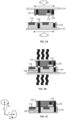
- Figures 4A-4D are schematic diagrams illustrating an example method for die bonding with radiation mediated release.
- Figures 4A-4D are cross-sectional views of bonding of a donor die (e.g., donor die 402) to a target die (e.g., target die 404) by radiation-mediated release.
- Figures 4A-4D are described with reference to "donor die” and "target die", which are relative descriptors as used herein and donor die may instead be target die and vice versa.
- a donor die may instead be a donor substrate and a target die may instead be a target substrate and a donor die may be bonded to a target substrate, a donor substrate may be bonded to a target substrate, and a donor substrate may be bonded to a target die.
- Multiple donor dies may be bonded to a single target die and vice versa.
- Radiation-mediated release may be used with any appropriate die bonding method, such as any of those previously described.
- the donor die 402 is supported by a carrier structure 414.
- the carrier structure 414 is transparent to at least a range of radiation (e.g., electromagnetic radiation, visible light, UV radiation, a particle or electron beam, etc.).
- the carrier structure 414 may be transparent to visible light, infrared radiation, ultraviolet radiation, a particle or electron beam, etc.
- the carrier structure 414 may be fabricated of any appropriate material, such as glass, silicon dioxide, sapphire, acrylic, etc.
- the carrier structure 414 may be a flexible substrate, such as a flexible polymer supported by a superstructure (such as a substrate chuck with one or more radiation windows).
- the carrier structure 414 may be a substantially inflexible substrate.
- the thickness of the carrier structure 414 (e.g., in the Z direction) may vary depending on which type of material the carrier structure 414 is fabricated from, such as where thickness may be selected based on deformation thresholds, electromagnetic radiation extinction coefficients, etc.
- the donor die 402 is adhered to the carrier structure 414 by, e.g., a layer of adhesive 450.
- adherered encompasses holding of one material to another in a manner which is releasable, including where the release is chemically, physically, electrically, etc. mediated.
- the adhesive 450 may be any appropriate adhesive, such as an organic glue, a polymer glue, etc.
- the adhesive 450 may be applied to the carrier structure 414 (such as by spin coating) and then the donor die 402 applied to the adhesive 450 on the substrate.
- the adhesive 450 may be applied to a surface of the donor die 402 (such as by ink jetting, dipping, etc.) and then the donor die 402 and adhesive 450 transferred to the carrier structure 414.
- the adhesive 450 may be of any appropriate thickness.
- the adhesive 450 may be an adhesive which forms a gas when exposed to radiation or heat.
- the adhesive 450 may be an adhesive which experiences a phase change (such as at atmospheric temperature and pressure) from solid or liquid to gas when excited by a burst of radiation or heated by such a burst of radiation.
- the adhesive 450 may be an adhesive which experiences a chemical change (such as a decomposition) which forms gas when excited by a burst of radiation or heated by such a burst.
- the adhesive 450 may expand in volume without forming a gas or only partially forming a gas when exposed to radiation or heat.
- the adhesive 450 may contain a dissolved gas which may partially precipitate when exposed to radiation or heat and which may create bubbles within the adhesive 450 thereby increasing the volume occupied by the adhesive.
- the adhesive 450 may be any appropriate material which experiences radiation-mediated volume expansion.
- the carrier structure 414 may be transparent to radiation of a wavelength which causes radiation-mediated volume expansion in the adhesive 450.
- the donor die 402 is aligned with the target die 404.
- the alignment may be performed by any appropriate method, such as any of those previously described.
- An alignment point 403 of the donor die 402 may be aligned with an alignment point 405 of the donor die 404 to become aligned as shown by alignment 407.
- the alignment may be accomplished by movement of the carrier structure 414 supporting the donor die 402 and/or by a carrier structure 416 supporting the target die 404.
- the donor die 402 may be prepared for bonding with the target die 404 (and vice versa) such as by atomic level cleaning and flatness treatment.
- the donor die 402 and the target die 404 may bond with each other by, e.g., Van der Waals bonding when brought into proximity (e.g., to within the order of a van der Waals contact distance, such as within twice the van der Waals contact distance but larger than once the van der Waals contact distance) and with sufficient other conditions, such as matching shape (which need to be flat), smoothness, etc.
- the donor die 402 and the target die 404 may be subsequently annealed (e.g., heated) to create or enhance an electrical bond between regions of the donor die 402 and the target die 404 (such as described in reference to Figures 1A-1C ).
- radiation 420 is applied to the adhesive 450.
- the radiation 420 may be a burst of radiation (e.g., a shot of radiation), which may be applied to the adhesive 450 to initiate the radiation-mediated bonding process or throughout the radiation-mediated bonding process.
- the radiation 420 may be part of a larger radiation pattern, which may be non-uniform over the donor die 402, over the carrier structure 414, etc.
- the radiation 420 may be directed at a central portion of the donor die, at an edge or corner of the donor die, etc.
- the radiation 420 may be a scanning beam, i.e., there is relative movement between the radiation 420 and the donor die 402.
- the radiation 420 may be variable, such as a subject to Gaussian intensity variation.
- the radiation 420 may be applied in a direction 422 substantially perpendicular (e.g., within 10 degrees thereof) to the carrier structure 414 (e.g., substantially perpendicular to a planar face of the donor die 402 in contact with the adhesive 450).
- the "rolling on” can be from one edge of the donor die toward another edge of the donor die or can be outwards from a central portion of the donor die to one or more edges of the donor die as depicted in Figures 4C and 4D .
- the application of the radiation 420 to the adhesive 450 may generate a gas (or other volumetric expansion as previously described) "bubble", such as bubble 452.
- the bubble 452 may occupy the entire thickness of the adhesive 450 (e.g., the entire adhesive layer may be decomposed into gas) or a partial thickness of the adhesive 450 (e.g., as depicted).
- the bubble 452 may cause deformation of the backside 454 of the donor die 402 (e.g., the face of the donor die 402 in contact with the adhesive 450).
- the bubble 452 may also cause deformation of the frontside 456 of the donor die 402, which may approach the target die 404 because of the deformation.
- the deformation of the donor die 402 may depend on the thickness of the adhesive 450 and the amount of adhesive 450 decomposed to gas or volumetrically expanded as well as the thickness and size of the donor die 402. For example, a 3 by 3 mm die of 1.5 ⁇ m thickness may experience up to 4 ⁇ m of bending (e.g., in the Z direction) due to 1 Pa of pressure created in the bubble 452.
- a donor die is selected from the plurality of donor dies.
- the donor die may be selected based on position (e.g., along a row, along a column), displacement (e.g., donor die closest to an ideal position), thickness (e.g., thicker dies may be placed before thinner dies, including if donor dies include two or more types of dies), etc.
- the donor die may have a corresponding target die, such as a target die in a corresponding location on a target substrate (e.g., target die carrier structure).
- a target die may be selected, by any appropriate method, and a donor die selected based on its correspondence to the selected target die.
- method 600 (and/or the other methods and systems described herein) is configured for die placement.
- Figure 7 is a flowchart which illustrates an exemplary method of radiation mediated die release. Each of these operations is described in detail below.
- the operations of method 700 presented below are intended to be illustrative. In some embodiments, method 700 may be accomplished with one or more additional operations not described, and/or without one or more of the operations discussed. Additionally, the order in which the operations of method 700 are illustrated in Figure 7 and described below is not intended to be limiting.
- one or more portions of method 700 may be implemented (e.g., by simulation, modeling, etc.) in one or more processing devices (e.g., one or more processors).
- the one or more processing devices may include one or more devices executing some or all of the operations of method 700 in response to instructions stored electronically on an electronic storage medium.
- the one or more processing devices may include one or more devices configured through hardware, firmware, and/or software to be specifically designed for execution of one or more of the operations of method 700, for example.
- a donor die is placed on a carrier structure using an adhesive which is convertible to gas or otherwise susceptible to volumetric expansion.
- the donor die may be any appropriate donor die, as previously discussed.
- the donor die may be a flexible die.
- the donor die may be substantially inflexible and a flexible interposer may be used between the donor die and the adhesive, as previously discussed in relation to Figures 5A-5D .
- the carrier structure may be any appropriate structure, including one fully or partially transparent to electromagnetic radiation, electron or particle beams, etc., as previously discussed.
- the carrier structure can be made of a transparent material and/or have open areas to allow radiation to pass.
- the adhesive may be any appropriate adhesive, which may be volumetrically altered by application of radiation or heat associated with radiation, such as by phase change, decomposition, precipitation, etc.
- the donor die may be placed on the carrier structure by any appropriate method, such as by a pick and place tool, by a dicing tool, etc.
- the donor die is aligned with a target die.
- the donor die may be aligned with the target die based on measurements of the location of the donor die (such as with respect to a carrier structure, a holder of the carrier structure, etc.) and/or the location of the target die (such as with respect to a carrier structure, a chuck, a semiconductor substrate where the target die is formed therein, etc.).
- the donor die and the target die may be aligned by any appropriate method, including any of those previously discussed.
- the donor die and the target die are brought into proximity with each other (e.g., by moving the donor die, by moving the target die, or both).
- the donor die may be in a proximity of within 3 ⁇ m of the target die, or within 1 ⁇ m of the target die, or within 500 nm of the target die, or within 200 nm of the target die, or within 100 nm of the target die, or within 50 nm of the target die.
- the separation between the donor die and target die may depend on the amount of flexion in the donor die (or flexible interposer).
- the donor die is held outside of the van der Waals force range of attraction with the target die.
- radiation is supplied through the carrier structure to the adhesive on the donor die (or flexible interposer).
- the radiation may be shaped to pinpoint one donor die at a time.
- the radiation spot size may be substantially smaller than the size of the donor die.
- the radiation may be directed at a central portion of the donor die, at an edge or corner of the donor die, etc.
- the radiation may be moved across the donor die.
- the radiation may function to cause the adhesive to decompose into at least a gaseous portion or otherwise volumetrically expand.
- the radiation may function to change the adhesive from a solid or liquid to a gas.
- the radiation may function to thermally expand the adhesive.
- the radiation may change the volume of the adhesive, in a region of the adhesive smaller in area than the target die, by any appropriate manner.
- the radiation may change the volume of the adhesive in an area which may be the same size as or larger than the donor die, such as if the volumetric expansion does not accompany a gaseous phase.
- a bonding wavefront may expand across a region to enable contact bonding of the donor die to the target die by, e.g., van der Waals forces.
- the efficiency of the bonding between the donor die and target die may be affected by smoothness (e.g., at the atomic level) and/or cleanliness (e.g., of dangling hydrogen bonds on the surface) of the donor die and/or target die.
- the combined donor and target die may be annealed as described herein to create or enhance one or more electrical connections.
- a subsequent donor die may be bonded to a subsequent target die, such as by repetition of operation 720 et seq.
- the subsequent donor die and target die may be bonded, including electrically, annealed or otherwise treated as described herein.
- method 700 (and/or the other methods and systems described herein) is configured for radiation mediated die release.
- the techniques and apparatus herein can be applied to die to die bonding, substrate to substrate bonding, die to substrate bonding, etc.
- the techniques and apparatus herein can be applied to bonding an individual donor die to an individual target die.
- the techniques and apparatus herein can be applied to bonding a group of donor dies to one or more target dies at a substantially same time or a group of target dies to one or more donor dies at a substantially same time.
- the techniques and apparatus herein can be applied to bonding one or more donor dies to a substrate comprising one or more target dies formed therein or thereon or bonding one or more target dies to a substrate comprising one or more donor dies formed therein or thereon.
- FIG. 8 is a diagram of an example computer system CS that may be used to implement one or more of the operations described herein.
- Computer system CS includes a bus BS or other communication mechanism for communicating information, and a processor PRO (or multiple processors) coupled with bus BS for processing information.
- Computer system CS also includes a main memory MM, such as a random-access memory (RAM) or other dynamic storage device, coupled to bus BS for storing information and instructions to be executed by processor PRO.
- Main memory MM also may be used for storing temporary variables or other intermediate information during execution of instructions by processor PRO.
- Computer system CS further includes a read only memory (ROM) ROM or other static storage device coupled to bus BS for storing static information and instructions for processor PRO.
- a storage device SD such as a magnetic disk or optical disk, is provided and coupled to bus BS for storing information and instructions.
Landscapes
- Container, Conveyance, Adherence, Positioning, Of Wafer (AREA)
Priority Applications (5)
| Application Number | Priority Date | Filing Date | Title |
|---|---|---|---|
| EP23220056.8A EP4576084A1 (de) | 2023-12-22 | 2023-12-22 | System und verfahren zum chipbonden mit strahlungsfreisetzung |
| PCT/EP2024/083262 WO2025131545A1 (en) | 2023-12-22 | 2024-11-22 | Apparatus and method for multi-stage die bonding |
| PCT/EP2024/083252 WO2025131543A1 (en) | 2023-12-22 | 2024-11-22 | Sensor and method for qualification of a topography of a surface of a die for die bonding |
| PCT/EP2024/084913 WO2025131758A1 (en) | 2023-12-22 | 2024-12-05 | System and method for die bonding with radiation release |
| TW113148303A TW202532811A (zh) | 2023-12-22 | 2024-12-12 | 用於針對晶粒接合之晶粒的表面形貌進行驗證之感測器及方法 |
Applications Claiming Priority (1)
| Application Number | Priority Date | Filing Date | Title |
|---|---|---|---|
| EP23220056.8A EP4576084A1 (de) | 2023-12-22 | 2023-12-22 | System und verfahren zum chipbonden mit strahlungsfreisetzung |
Publications (1)
| Publication Number | Publication Date |
|---|---|
| EP4576084A1 true EP4576084A1 (de) | 2025-06-25 |
Family
ID=89321428
Family Applications (1)
| Application Number | Title | Priority Date | Filing Date |
|---|---|---|---|
| EP23220056.8A Pending EP4576084A1 (de) | 2023-12-22 | 2023-12-22 | System und verfahren zum chipbonden mit strahlungsfreisetzung |
Country Status (1)
| Country | Link |
|---|---|
| EP (1) | EP4576084A1 (de) |
Citations (2)
| Publication number | Priority date | Publication date | Assignee | Title |
|---|---|---|---|---|
| US20230245996A1 (en) * | 2021-03-29 | 2023-08-03 | Board Of Regents, The University Of Texas System | Processes and applications for catalyst influenced chemical etching |
| US20230352615A1 (en) * | 2021-12-15 | 2023-11-02 | Imec Vzw | Method for Bonding Dies to a Carrier Substrate |
-
2023
- 2023-12-22 EP EP23220056.8A patent/EP4576084A1/de active Pending
Patent Citations (2)
| Publication number | Priority date | Publication date | Assignee | Title |
|---|---|---|---|---|
| US20230245996A1 (en) * | 2021-03-29 | 2023-08-03 | Board Of Regents, The University Of Texas System | Processes and applications for catalyst influenced chemical etching |
| US20230352615A1 (en) * | 2021-12-15 | 2023-11-02 | Imec Vzw | Method for Bonding Dies to a Carrier Substrate |
Similar Documents
| Publication | Publication Date | Title |
|---|---|---|
| TWI517290B (zh) | A substrate position alignment device, a substrate alignment method, and a manufacturing method of a multilayer semiconductor | |
| JP7147778B2 (ja) | 積層基板の製造方法、および製造装置 | |
| KR20240169682A (ko) | W2w 접합을 위한 웨이퍼 형상 제어 | |
| CN109314069B (zh) | 用于部件堆叠和/或拾放过程的微型多拾取元件 | |
| US12447728B2 (en) | Bonding method and bonding device | |
| EP4576084A1 (de) | System und verfahren zum chipbonden mit strahlungsfreisetzung | |
| KR20200110802A (ko) | 위치 맞춤 방법 및 위치 맞춤 장치 | |
| WO2025131758A1 (en) | System and method for die bonding with radiation release | |
| Ip et al. | Overlay performance in permanent bonded wafer integration schemes | |
| WO2025252364A1 (en) | System and method for die bonding self-alignment | |
| EP4575389A1 (de) | Sensor und verfahren zur qualifizierung einer topographie einer oberfläche einer matrize zum chipbonden | |
| EP4579723A1 (de) | Vorrichtung und verfahren zum mehrstufigen chipbonden | |
| JP2006100656A (ja) | ウェハ積層時の重ね合わせ方法 | |
| WO2025252363A1 (en) | System and method for die bonding alignment referenced to carrier position | |
| WO2025131545A1 (en) | Apparatus and method for multi-stage die bonding | |
| WO2025171976A1 (en) | Apparatus and method for securing a die for die bonding | |
| WO2025131543A1 (en) | Sensor and method for qualification of a topography of a surface of a die for die bonding | |
| EP4576085A1 (de) | System und verfahren zur spannungsfreisetzung beim chipbonden | |
| JP7786482B2 (ja) | 基板補正装置、基板積層装置、基板処理システム、基板補正方法、基板処理方法、および半導体装置の製造方法 | |
| WO2025233063A1 (en) | System and method for die bonding with diffraction based alignment marks on the die | |
| JP2012185400A (ja) | 収納容器、デバイス製造装置及びデバイス製造方法 | |
| WO2025242350A1 (en) | Apparatus and method for continuous die bonding | |
| WO2025190610A1 (en) | Apparatus and method for removing gaseous byproduct of die bonding | |
| JP2024060959A (ja) | 接合装置、接合方法及び物品の製造方法 | |
| CN100521142C (zh) | 晶片载具 |
Legal Events
| Date | Code | Title | Description |
|---|---|---|---|
| PUAI | Public reference made under article 153(3) epc to a published international application that has entered the european phase |
Free format text: ORIGINAL CODE: 0009012 |
|
| STAA | Information on the status of an ep patent application or granted ep patent |
Free format text: STATUS: THE APPLICATION HAS BEEN PUBLISHED |
|
| AK | Designated contracting states |
Kind code of ref document: A1 Designated state(s): AL AT BE BG CH CY CZ DE DK EE ES FI FR GB GR HR HU IE IS IT LI LT LU LV MC ME MK MT NL NO PL PT RO RS SE SI SK SM TR |