EP4567893A1 - Anzeigetafel und anzeigevorrichtung - Google Patents
Anzeigetafel und anzeigevorrichtung Download PDFInfo
- Publication number
- EP4567893A1 EP4567893A1 EP23914000.7A EP23914000A EP4567893A1 EP 4567893 A1 EP4567893 A1 EP 4567893A1 EP 23914000 A EP23914000 A EP 23914000A EP 4567893 A1 EP4567893 A1 EP 4567893A1
- Authority
- EP
- European Patent Office
- Prior art keywords
- line
- transistor
- coupled
- node
- initialization
- Prior art date
- Legal status (The legal status is an assumption and is not a legal conclusion. Google has not performed a legal analysis and makes no representation as to the accuracy of the status listed.)
- Pending
Links
Images


Classifications
-
- H—ELECTRICITY
- H10—SEMICONDUCTOR DEVICES; ELECTRIC SOLID-STATE DEVICES NOT OTHERWISE PROVIDED FOR
- H10K—ORGANIC ELECTRIC SOLID-STATE DEVICES
- H10K59/00—Integrated devices, or assemblies of multiple devices, comprising at least one organic light-emitting element covered by group H10K50/00
- H10K59/10—OLED displays
- H10K59/12—Active-matrix OLED [AMOLED] displays
- H10K59/131—Interconnections, e.g. wiring lines or terminals
-
- G—PHYSICS
- G09—EDUCATION; CRYPTOGRAPHY; DISPLAY; ADVERTISING; SEALS
- G09G—ARRANGEMENTS OR CIRCUITS FOR CONTROL OF INDICATING DEVICES USING STATIC MEANS TO PRESENT VARIABLE INFORMATION
- G09G3/00—Control arrangements or circuits, of interest only in connection with visual indicators other than cathode-ray tubes
- G09G3/20—Control arrangements or circuits, of interest only in connection with visual indicators other than cathode-ray tubes for presentation of an assembly of a number of characters, e.g. a page, by composing the assembly by combination of individual elements arranged in a matrix no fixed position being assigned to or needed to be assigned to the individual characters or partial characters
- G09G3/22—Control arrangements or circuits, of interest only in connection with visual indicators other than cathode-ray tubes for presentation of an assembly of a number of characters, e.g. a page, by composing the assembly by combination of individual elements arranged in a matrix no fixed position being assigned to or needed to be assigned to the individual characters or partial characters using controlled light sources
- G09G3/30—Control arrangements or circuits, of interest only in connection with visual indicators other than cathode-ray tubes for presentation of an assembly of a number of characters, e.g. a page, by composing the assembly by combination of individual elements arranged in a matrix no fixed position being assigned to or needed to be assigned to the individual characters or partial characters using controlled light sources using electroluminescent panels
- G09G3/32—Control arrangements or circuits, of interest only in connection with visual indicators other than cathode-ray tubes for presentation of an assembly of a number of characters, e.g. a page, by composing the assembly by combination of individual elements arranged in a matrix no fixed position being assigned to or needed to be assigned to the individual characters or partial characters using controlled light sources using electroluminescent panels semiconductive, e.g. using light-emitting diodes [LED]
- G09G3/3208—Control arrangements or circuits, of interest only in connection with visual indicators other than cathode-ray tubes for presentation of an assembly of a number of characters, e.g. a page, by composing the assembly by combination of individual elements arranged in a matrix no fixed position being assigned to or needed to be assigned to the individual characters or partial characters using controlled light sources using electroluminescent panels semiconductive, e.g. using light-emitting diodes [LED] organic, e.g. using organic light-emitting diodes [OLED]
- G09G3/3225—Control arrangements or circuits, of interest only in connection with visual indicators other than cathode-ray tubes for presentation of an assembly of a number of characters, e.g. a page, by composing the assembly by combination of individual elements arranged in a matrix no fixed position being assigned to or needed to be assigned to the individual characters or partial characters using controlled light sources using electroluminescent panels semiconductive, e.g. using light-emitting diodes [LED] organic, e.g. using organic light-emitting diodes [OLED] using an active matrix
- G09G3/3233—Control arrangements or circuits, of interest only in connection with visual indicators other than cathode-ray tubes for presentation of an assembly of a number of characters, e.g. a page, by composing the assembly by combination of individual elements arranged in a matrix no fixed position being assigned to or needed to be assigned to the individual characters or partial characters using controlled light sources using electroluminescent panels semiconductive, e.g. using light-emitting diodes [LED] organic, e.g. using organic light-emitting diodes [OLED] using an active matrix with pixel circuitry controlling the current through the light-emitting element
-
- G—PHYSICS
- G09—EDUCATION; CRYPTOGRAPHY; DISPLAY; ADVERTISING; SEALS
- G09G—ARRANGEMENTS OR CIRCUITS FOR CONTROL OF INDICATING DEVICES USING STATIC MEANS TO PRESENT VARIABLE INFORMATION
- G09G2300/00—Aspects of the constitution of display devices
- G09G2300/04—Structural and physical details of display devices
- G09G2300/0421—Structural details of the set of electrodes
- G09G2300/0426—Layout of electrodes and connections
-
- G—PHYSICS
- G09—EDUCATION; CRYPTOGRAPHY; DISPLAY; ADVERTISING; SEALS
- G09G—ARRANGEMENTS OR CIRCUITS FOR CONTROL OF INDICATING DEVICES USING STATIC MEANS TO PRESENT VARIABLE INFORMATION
- G09G2300/00—Aspects of the constitution of display devices
- G09G2300/08—Active matrix structure, i.e. with use of active elements, inclusive of non-linear two terminal elements, in the pixels together with light emitting or modulating elements
- G09G2300/0809—Several active elements per pixel in active matrix panels
- G09G2300/0819—Several active elements per pixel in active matrix panels used for counteracting undesired variations, e.g. feedback or autozeroing
-
- G—PHYSICS
- G09—EDUCATION; CRYPTOGRAPHY; DISPLAY; ADVERTISING; SEALS
- G09G—ARRANGEMENTS OR CIRCUITS FOR CONTROL OF INDICATING DEVICES USING STATIC MEANS TO PRESENT VARIABLE INFORMATION
- G09G2300/00—Aspects of the constitution of display devices
- G09G2300/08—Active matrix structure, i.e. with use of active elements, inclusive of non-linear two terminal elements, in the pixels together with light emitting or modulating elements
- G09G2300/0809—Several active elements per pixel in active matrix panels
- G09G2300/0842—Several active elements per pixel in active matrix panels forming a memory circuit, e.g. a dynamic memory with one capacitor
- G09G2300/0861—Several active elements per pixel in active matrix panels forming a memory circuit, e.g. a dynamic memory with one capacitor with additional control of the display period without amending the charge stored in a pixel memory, e.g. by means of additional select electrodes
-
- G—PHYSICS
- G09—EDUCATION; CRYPTOGRAPHY; DISPLAY; ADVERTISING; SEALS
- G09G—ARRANGEMENTS OR CIRCUITS FOR CONTROL OF INDICATING DEVICES USING STATIC MEANS TO PRESENT VARIABLE INFORMATION
- G09G2310/00—Command of the display device
- G09G2310/02—Addressing, scanning or driving the display screen or processing steps related thereto
- G09G2310/0243—Details of the generation of driving signals
- G09G2310/0251—Precharge or discharge of pixel before applying new pixel voltage
-
- G—PHYSICS
- G09—EDUCATION; CRYPTOGRAPHY; DISPLAY; ADVERTISING; SEALS
- G09G—ARRANGEMENTS OR CIRCUITS FOR CONTROL OF INDICATING DEVICES USING STATIC MEANS TO PRESENT VARIABLE INFORMATION
- G09G2310/00—Command of the display device
- G09G2310/02—Addressing, scanning or driving the display screen or processing steps related thereto
- G09G2310/0243—Details of the generation of driving signals
- G09G2310/0254—Control of polarity reversal in general, other than for liquid crystal displays
- G09G2310/0256—Control of polarity reversal in general, other than for liquid crystal displays with the purpose of reversing the voltage across a light emitting or modulating element within a pixel
-
- H—ELECTRICITY
- H10—SEMICONDUCTOR DEVICES; ELECTRIC SOLID-STATE DEVICES NOT OTHERWISE PROVIDED FOR
- H10H—INORGANIC LIGHT-EMITTING SEMICONDUCTOR DEVICES HAVING POTENTIAL BARRIERS
- H10H29/00—Integrated devices, or assemblies of multiple devices, comprising at least one light-emitting semiconductor element covered by group H10H20/00
- H10H29/30—Active-matrix LED displays
- H10H29/39—Connection of the pixel electrodes to the driving transistors
-
- H—ELECTRICITY
- H10—SEMICONDUCTOR DEVICES; ELECTRIC SOLID-STATE DEVICES NOT OTHERWISE PROVIDED FOR
- H10K—ORGANIC ELECTRIC SOLID-STATE DEVICES
- H10K59/00—Integrated devices, or assemblies of multiple devices, comprising at least one organic light-emitting element covered by group H10K50/00
- H10K59/30—Devices specially adapted for multicolour light emission
- H10K59/35—Devices specially adapted for multicolour light emission comprising red-green-blue [RGB] subpixels
Definitions
- the present disclosure relates to the field of display technologies, and in particular, to a display panel and a display device.
- OLED display panels are widely used in various display devices because of their advantages of self-illumination, fast response speed, low power consumption and the like.
- an OLED display panel generally includes a substrate and a plurality of pixels disposed on the substrate.
- Each pixel includes a pixel circuit and a light-emitting element.
- the pixel circuit includes a driving transistor.
- the pixel circuit is coupled to a plurality of signal lines and the light-emitting element.
- the pixel circuit is configured to generate, based on signals provided by the plurality of signal lines, driving current through a driving transistor and transmit the driving current to the light-emitting element to drive the light-emitting element to emit light.
- the electrodes of the driving transistor in the pixel circuit have different voltages, when the OLED display panel switches display at different frequencies, the brightness difference is caused, and the display effect is poor.
- a display panel and a display device are provided.
- the technical solutions are as follows.
- a display panel includes:
- the pixel circuit further includes:
- the substrate has a display region; wherein at least part of the second power line is disposed in the display region, and the part of the second power line disposed in the display region is mesh-shaped.
- the signal line coupled to each sub-pixel has a first portion extending along a first direction, and the first portions of the signal line coupled to the plurality of sub-pixels in each pixel are communicated with each other in the first direction, the signal line coupled to at least one sub-pixel has a second portion extending along a second direction, and the second portions of the signal line coupled to different sub-pixels are spaced apart from each other in the first direction, and the first portion and the second portion are coupled to each other; and for at least part of the mesh-shaped signal lines, the first portion and the second portion are disposed in different layers, and for other mesh-shaped signal lines except the at least part of the mesh-shaped signal lines, the first portion and the second portion of each of the signal lines are disposed in a same layer;
- At least two of the first initialization line, the second initialization line and the third initialization line are mesh-shaped; and each pixel includes at least three sub-pixels; wherein for each of the at least two mesh-shaped initialization lines, the initialization line coupled to one of the at least three sub-pixels has the second portion.
- different sub-pixels are coupled to different initialization lines having the second portion.
- At least two of the first initialization line, the second initialization line and the third initialization line are mesh-shaped; and each pixel includes at least three sub-pixels; wherein for each of the at least two mesh-shaped initialization lines, the initialization line coupled to partial sub-pixels of the at least three sub-pixels has the second portion.
- a number of the partial sub-pixels is greater than or equal to 1, and the partial sub-pixels are not adjacent in the first direction; and two sub-pixels adjacent in the first direction are coupled to different initialization lines having the second portion.
- At least two of the first initialization line, the second initialization line and the third initialization line are mesh-shaped; and each pixel includes at least three sub-pixels; wherein for one part of the at least two mesh-shaped initialization lines, the initialization line coupled to each sub-pixel of the at least three sub-pixels has the second portion, and for the other part of the at least two mesh-shaped initialization lines except the one part of the at least two mesh-shaped initialization lines, the initialization line coupled to partial sub-pixels of the at least three sub-pixels has the second portion.
- a number of the partial sub-pixels is greater than or equal to 1, and the partial sub-pixels are not adjacent in the first direction.
- each pixel includes three sub-pixels or four sub-pixels; each of the first initialization line, the second initialization line and the third initialization line is mesh-shaped; or, the second initialization line and the third initialization line are mesh-shaped.
- the three sub-pixels in each pixel include: one red sub-pixel, one green sub-pixel and one blue sub-pixel; and the four sub-pixels in each pixel include: one red sub-pixel, two green sub-pixels and one blue sub-pixel.
- the pixel in the display panel includes: a plurality of metal layers sequentially stacked in a direction going away from the substrate; wherein
- the first portion is disposed in a same layer as one metal layer of the plurality of metal layers, and the second portion is disposed in a same layer as another metal layer of the plurality of metal layers; and for the other mesh-shaped signal lines except the at least part of the mesh-shaped signal lines, the first portion and the second portion are disposed in a same layer as a same metal layer of the plurality of metal layers; each of the other signal lines is disposed in a same layer as any metal layer of the plurality of metal layers.
- the plurality of metal layers include: a first gate metal layer, a second gate metal layer, a third gate metal layer, a first source-drain metal layer and a second source-drain metal layer which are sequentially stacked;
- the light emission control line extends along the first direction, and is disposed in a same layer as the first gate metal layer;
- the first initialization line extends along the first direction, and is disposed in a same layer as the second gate metal layer;
- the mesh-shaped signal lines further include: a second power line disposed in a display region of the substrate; wherein a first portion of the second power line is disposed in a same layer as the first source-drain metal layer, and a second portion of the second power line is disposed in a same layer as the second source-drain metal layer.
- the second power line disposed in the display region of the substrate extends along the second direction, and is disposed in a same layer as the second source-drain metal layer;
- the mesh-shaped signal lines further include: the first initialization line; wherein a first portion of the first initialization line is disposed in a same layer as the second gate metal layer, and a second portion of the first initialization line is disposed in a same layer as the second source-drain metal layer.
- the light emission control circuit includes: a first transistor, a second transistor, a third transistor, a fourth transistor and a storage capacitor; the reset circuit includes: a fifth transistor, a sixth transistor and a seventh transistor; and the drive circuit includes an eighth transistor;
- the second transistor is an N-type oxide transistor; and the first transistor, the third transistor, the fourth transistor, the fifth transistor, the sixth transistor, the seventh transistor and the eighth transistor are P-type low-temperature poly-silicon transistors.
- a display device in another aspect, includes: a power supply assembly, and the display panel described in the above aspect; wherein the power supply assembly is coupled to the display panel, and configured to supply power to the display panel.
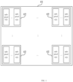
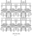
- FIG. 1 is a schematic structural diagram of a display panel according to some embodiments of the present disclosure.
- the display panel includes a substrate 01 and a plurality of pixels 02 disposed on the substrate 01.
- Each of the pixels 02 includes a plurality of sub-pixels 021.
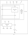
- each sub-pixel 021 includes a pixel circuit P1 and a light-emitting element L1, and the pixel circuit P1 includes a drive circuit P11 and a reset circuit P12.
- the drive circuit P11 is coupled to (i.e., electrically connected to) a first node N1, a second node N2 and a third node N3.
- the drive circuit P11 is configured to control a potential of the second node N2 based on a potential of the third node N3 and a potential of the first node N1.
- the drive circuit P11 when applied to the OLED display panel, the drive circuit P11 generates a light emission driving signal (i.e., driving current) for driving the OLED to emit light based on the potential of the third node N3 and the potential of the first node N1, and transmit the light emission driving signal to the second node N2.
- a light emission driving signal i.e., driving current
- the second node N2 is connected to the light-emitting element L1
- the light emission driving signal is further transmitted to the light-emitting element L1 to drive the light-emitting element L1 to emit light.
- the reset circuit P12 is coupled to a first reset line R1, a second reset line R2, a first initialization line Vinit1, a second initialization line Vinit2, a third initialization line Vinit3 (which is also referred to as a reference power line Vref), the first node N1, the second node N2, and a first electrode of the light-emitting element L1 which are disposed on the substrate 01.
- the reset circuit P12 is configured to control the connection or disconnection between the first initialization line Vinit1 and the second node N2 based on a first reset signal provided by the first reset line R1, and control, based on a second reset signal provided by the second reset line R2, the connection or disconnection between the second initialization line Vinit2 and the first electrode of the light-emitting element L1 and the connection or disconnection between the third initialization line Vinit3 and the first node N1.
- the node coupled to the first electrode of the light-emitting element L1 is marked with a fourth node N4.
- the reset circuit P12 controls the first initialization line Vinit1 to be connected to the second node N2 when the potential of the first reset signal provided by the first reset line R1 is a first potential.
- a first initialization signal provided by the first initialization line Vinit1 is transmitted to the second node N2, thereby resetting the second node N2.
- the first initialization signal is further transmitted to the third node N3, thereby resetting the third node N3.
- the reset circuit P12 controls the first initialization line Vinit1 to be disconnected from the second node N2 when the potential of the first reset signal provided by the first reset line R1 is a second potential.
- the reset circuit P12 controls the second initialization line Vinit2 to be connected to the first electrode of the light-emitting element L1, and controls the third initialization line Vinit3 to be connected to the first node N1.
- a second initialization signal provided by the second initialization line Vinit2 is transmitted to the first electrode of the light-emitting element L1, thereby resetting the first electrode of the light-emitting element L1
- a third initialization signal provided by the third initialization line Vinit3 is transmitted to the first node N1, thereby resetting the first node N1.
- the reset circuit P12 controls the second initialization line Vinit2 to be disconnected from the first electrode of the light-emitting element L1 and controls the third initialization line Vinit3 to be disconnected from the first node N1.
- the reset circuit P12 resets the first node N1, the second node N2, the third node N3 and the first electrode of the light-emitting element L1 (i.e., the fourth node N4 in FIG. 2 ).
- the current reset circuit can only reset the third node N3 and the fourth node N4, but cannot reset the first node N1 and the second node N2.
- the variable refresh rate (VRR) is poor, resulting in a brightness difference, and human eyes can observe brightness flickers.
- VRR variable refresh rate
- the third node N3 is reset to bias the driving transistor, and at different grayscales, different potentials are written into the first node N1, the bias potentials are different at different grayscales, the bias effect is poor, and the driving transistor has hysteresis.
- the reset circuit P12 is configured to reset the third node N3 and the first electrode (i.e., the fourth node N4) of the light-emitting element L1, and reset the first node N1 and the second node N2, so that the potential of the first node N1 and the potential of the second node N2 remain consistent in the refresh frame and the hold frame.
- the driving transistor can be biased more flexibly to solve the hysteresis problem of the driving transistor, but also the poor VRR can be effectively improved. Therefore, when the display panel switches the display between different frequencies, the brightness difference is small, and the display effect is better.
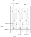
- At least one of the first initialization line Vinit1, the second initialization line Vinit2 and the third initialization line Vinit3 is mesh-shaped.
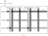
- the third initialization line Vinit3 is mesh-shaped.
- a meshed-shaped signal line includes two portions coupled to each other, and the two portions extend in two non-parallel directions, that is, the two portions intersect.
- the mesh-shaped third initialization line Vinit3 includes two portions Vinit3-1 and Vinit3-2 intersecting each other.
- the stability of the initialization signal provided by the initialization line (e.g., the third initialization signal provided by the third initialization line Vinit3) can be improved by setting the initialization line to be meshed. In this way, the node can be reset more reliably, thereby ensuring that the display panel has a better display effect.
- the embodiments of the present disclosure provide a display panel.
- the pixel circuit of each sub-pixel includes a drive circuit and a reset circuit.
- the drive circuit can control the potential of the second node based on the potential of the first node and the potential of the third node, and when the second node is connected to the light-emitting element, the potential transmitted by the drive circuit to the second node can drive the light-emitting element to emit light.
- the reset circuit can transmit an initialization signal to the first node, the second node and the light-emitting element, respectively, to reset the first node, the second node and the light-emitting element. In this way, the potentials of the nodes in the pixel circuit can keep consistent, and each pixel circuit can reliably drive the light-emitting element to emit light, thereby solving the brightness difference and ensuring a better display effect.
- At least one of the initialization lines which provide the initialization signals is set to be mesh-shaped, which can improve the stability of the initialization signal provided by the initialization line, thereby further ensuring a better display effect.
- the pixel circuit P1 described in the embodiments of the present disclosure further includes a light emission control circuit P13.
- the light emission control circuit P13 is coupled to a first gate line G1, a second gate line G2, a light emission control line EM, a data line D1, a first power line VDD, the first node N1, the second node N2, the third node N3 and the first electrode (i.e., the fourth node N4) of the light-emitting element L1 that are disposed on the substrate 01.
- the light emission control circuit P13 is configured to control the connection or disconnection between the data line D1 and the first node N1 based on a first gate driving signal provided by the first gate line G1, control the connection or disconnection between the second node N2 and the third node N3 based on a second gate driving signal provided by the second gate line G2, and control, based on a light emission control signal provided by the light emission control line EM, the connection or disconnection between the first power line VDD and the first node N1 and the control connection or disconnection between the second node N2 and the first electrode of the light-emitting element L1.
- the light emission control circuit P13 controls the data line D1 to be connected to the first node N1 when the potential of the first gate driving signal provided by the first gate line G1 is the first potential. In this case, the data signal provided by the data line D1 is further transmitted to the first node N1.
- the light emission control circuit P13 controls the data line D1 to be disconnected from the first node N1 when the potential of the first gate driving signal provided by the first gate line G1 is the second potential.
- the light emission control circuit P13 controls the second node N2 to be connected to the third node N3 when the potential of the second gate driving signal provided by the second gate line G2 is the first potential. In this case, the potential of the second node N2 and the potential of the third node N3 interact. The light emission control circuit P13 controls the second node N2 to be disconnected from the third node N3 when the potential of the second gate driving signal provided by the second gate line G2 is the second potential.
- the light emission control circuit P13 controls the first power line VDD to be connected to the first node N1, and controls the second node N2 to be connected to the first electrode (i.e., the fourth node N4) of the light-emitting element L1.
- the first power signal provided by the first power line VDD is further transmitted to the first node N1
- the signal transmitted to the second node N2 is further transmitted to the first electrode of the light-emitting element L1.
- the light emission control circuit P13 controls the first power line VDD to be disconnected from the first node N1, and controls the second node N2 to be disconnected from the first electrode of the light-emitting element L1.
- the second electrode of the light-emitting element L1 is coupled to a second power line VSS.
- the light-emitting element L1 is configured to emit light based on the potential of the first electrode and the potential of the second electrode.
- the light-emitting element L1 when the light-emitting element L1 is an OLED, the light-emitting element L1 emits light based on a voltage difference between the light emission driving signal transmitted by the pixel circuit P1 and the second power signal provided by the second power line VSS.
- one of the first electrode and the second electrode of the light-emitting element L1 is an anode, and the other electrode is a cathode.
- the embodiments of the present disclosure are described by taking an example where the first electrode is an anode and the second electrode is a cathode. On this basis, the potential of the first power signal provided by the first power line VDD is a high potential, and the potential of the second power signal provided by the second power line VSS is a low potential.
- the substrate 01 includes a display region AA, and includes a non-display region (not shown in the figure) adjacent to the display region AA.
- Each signal line coupled to the pixel circuit P1 shown in FIG. 2 is partially disposed in the non-display region, and partially disposed in the display region AA.
- the portion of the signal line disposed in the non-display region is configured to be coupled to a signal providing circuit, to receive a signal provided by the signal providing circuit.
- the first gate line G1 as an example, the part of the first gate line G1 disposed in the non-display region is coupled to the gate drive circuit, to receive the first gate driving signal transmitted by the gate drive circuit.
- the gate drive circuit is the signal providing circuit.
- the other signal lines are similar to the first gate line G1, and details are not described herein again.
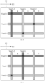
- the second power line VSS coupled to the light-emitting element L1 is generally disposed in the non-display region and disposed around the display region AA.
- the second power line VSS is disposed in the display region AA. That is, VSS in AA is designed.
- a shorter second power line VSS is provided to be coupled to the light-emitting element L1 in the display region AA, which can reduce the voltage drop (IR Drop) on the second power line VSS and ensure that the second power line VSS reliably provides the second power signal to the second electrode of the light-emitting element L1, thereby ensuring reliable light emission of the light-emitting element L1.
- the second power line VSS is also designed to be mesh-shaped. That is, like the third initialization line Vinit3, the second power line VSS also includes two portions which intersect and are coupled to each other. In this way, the stability of the second power supply signal provided by the second power line VSS can also be improved, and the light-emitting element L1 can emit light reliably, thereby further ensuring that the display panel has a better display effect.
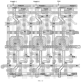
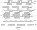
- FIG. 4 is a schematic structural diagram of another pixel circuit according to some embodiments of the present disclosure.
- the light emission control circuit P13 includes a first transistor T1, a second transistor T2, a third transistor T3, a fourth transistor T4 and a storage capacitor Cst.
- the reset circuit P12 includes a fifth transistor T5, a sixth transistor T6 and a seventh transistor T7.
- the drive circuit P11 includes an eighth transistor T8 (i.e., the driving transistor described in the foregoing embodiments).
- a gate of the first transistor T1 is coupled to the first gate line G1, a first electrode of the first transistor T1 is coupled to the data line D1, and a second electrode of the first transistor T1 is coupled to the first node N1.
- a gate of the second transistor T2 is coupled to the second gate line G2, a first electrode of the second transistor T2 is coupled to the second node N2, and a second electrode of the second transistor T2 is coupled to the third node N3.
- a gate of the third transistor T3 is coupled to the light emission control line EM, a first electrode of the third transistor T3 is coupled to the first power line VDD, and a second electrode of the third transistor T3 is coupled to the first node N1.
- a gate of the fourth transistor T4 is coupled to the light emission control line EM, a first electrode of the fourth transistor T4 is coupled to the second node N2, and a second electrode of the fourth transistor T4 is coupled to the first electrode (i.e., the fourth node N4) of the light-emitting element L1.
- One terminal of the storage capacitor Cst is coupled to the first power line VDD, and the other terminal of the storage capacitor Cst is coupled to the third node N3.
- a gate of the fifth transistor T5 is coupled to the first reset line R1, a first electrode of the fifth transistor T5 is coupled to the first initialization line Vinit1, and a second electrode of the fifth transistor T5 is coupled to the second node N2.
- a gate of the sixth transistor T6 is coupled to the second reset line R2, a first electrode of the sixth transistor T6 is coupled to the second initialization line Vinit2, and a second electrode of the sixth transistor T6 is coupled to the first electrode of the light-emitting element L1.
- a gate of the seventh transistor T7 is coupled to the second reset line R2, a first electrode of the seventh transistor T7 is coupled to the third initialization line Vinit3, and a second electrode of the seventh transistor T7 is coupled to the first node N1.
- a gate of the eighth transistor T8 is coupled to the third node N3, a first electrode of the eighth transistor T8 is coupled to the first node N1, and a second electrode of the eighth transistor T8 is coupled to the second node N2.
- the transistors used in all the embodiments of the present disclosure are fieldeffect transistors or other devices having the same characteristics.
- the transistors used in the embodiments of the present disclosure are mainly switching transistors according to the functions in the circuit. Since the source (S) and the drain (D) of the switching transistor used here are symmetrical, the source and the drain are interchangeable.
- the source is referred to as a first electrode
- the drain is referred to as a second electrode
- the drain is referred to as a first electrode
- the source is referred to as a second electrode.
- an intermediate terminal of the transistor is a gate
- a signal input terminal is the source
- a signal output terminal is the drain.
- the switching transistors used in the embodiments of the present disclosure include any one of a P-type switching transistor and an N-type switching transistor.
- the P-type switching transistor is turned on when the gate is at a low level and is turned off when the gate is at a high level
- the N-type switching transistor is turned on when the gate is at a high level and turned off when the gate is at a low level.
- the plurality of signals in various embodiments of the present disclosure each correspond to an effective potential and an ineffective potential.
- the effective potential and the ineffective potential only represent that the signal has potentials with two different state quantities, but do not represent that the effective potential or the ineffective potential has a specific value in the whole text.
- the second transistor T2 is an N-type oxide transistor; and the first transistor T1, the third transistor T3, the fourth transistor T4, the fifth transistor T5, the sixth transistor T6, the seventh transistor T7 and the eighth transistor T8 are P-type low-temperature poly-silicon (LTPS) transistors. That is, the second transistor T2 is an N-type transistor, and the N-type transistor is made from an oxide material; and the first transistor T1, the third transistor T3, the fourth transistor T4, the fifth transistor T5, the sixth transistor T6, the seventh transistor T7 and the eighth transistor T8 are P-type transistors, and the P-type transistor is made from LTPS.
- LTPS low-temperature poly-silicon
- the pixel circuit P1 shown in FIG. 4 is also referred to as an LTPO pixel circuit.
- all the transistors are P-type LTPS transistors, and accordingly, the pixel circuit including only the P-type transistors is also referred to as an LTPS pixel circuit.
- the structure shown in FIG. 4 is a pixel circuit having an 8T1C structure (i.e., including 8 transistors and 1 capacitors), the seventh transistor T7 is considered as a newly added transistor, and the coupling position of the fifth transistor T5 is adjusted relative to the current transistor which resets the third node N3.
- the second reset signal received by the gate of the seventh transistor T7 is a pulse signal.
- the 8T1C structure is also referred to as a 7T1C pulse structure.
- the pixel circuit P1 is not limited to the 8T1C structure shown in FIG. 4 , as long as the pixel circuit P1 includes the reset circuit P12 as shown in FIG. 4 .
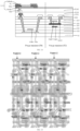
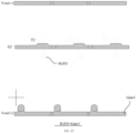
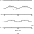
- FIG. 5 is a timing diagram of signal lines in a pixel circuit in a multi-frame refresh according to some embodiments of the present disclosure. As shown in FIG. 5 :
- the signal line coupled to each sub-pixel 021 has a first portion (e.g., Vinit3 -1) extending along the first direction X1, and the first portions of the signal line coupled to the plurality of sub-pixels 021 in each pixel 02 are communicated with each other in the first direction X1.
- Vinit3-1 of the third initialization line Vinit3 coupled to three sub-pixels 021 shown in FIG. 3 are communicated with each other in the first direction X1.
- the signal line coupled to at least one (i.e., one or more) sub-pixel 021 has a second portion (e.g., Vinit3-2) extending along the second direction X2, and the second portions of the signal line coupled to different sub-pixels 021 are spaced from each other in the first direction X1, that is, not communicated with each other. Moreover, the first portion and the second portion are coupled to each other. For a sub-pixel 021 which does not have the second portion, the first portion of the signal line is in communication with the first portion of another sub-pixel 021 so as to be coupled to the second portion of the sub-pixel 021 having the second portion. That is, in the embodiments of the present disclosure, the plurality of sub-pixels 021 share the second portion.
- the plurality of sub-pixels 021 each have the second portion.
- the first portion and the second portion of each of the signal lines are disposed in different layers.
- the first portion and the second portion of each of the signal lines are disposed in the same layer.
- each of the signal lines extends along the first direction X1 or the second direction X2.
- the second power line VSS shown in FIG. 3 extends along the second direction X2.
- the first direction X1 and the second direction X2 intersect.
- the first direction X1 and the second direction X2 are perpendicular to each other.
- the first direction X1 is the pixel row direction
- the second direction X2 is the pixel column direction.
- each pixel 02 includes at least three sub-pixels 021.
- each pixel 02 described in the embodiments of the present disclosure includes three sub-pixels 021.
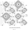
- the three sub-pixels 021 in each pixel 02 include a red (R) sub-pixel 021R, a green (G) sub-pixel 021G and a blue (B) sub-pixel 021B. That is, each pixel 02 has an RGB pixel structure, which is also referred to as a real RGB pixel structure.
- each pixel 02 described in the embodiments of the present disclosure includes four sub-pixels 021.
- the four sub-pixels 021 in each pixel 02 include one red sub-pixel 021R, two green sub-pixels 021G and one blue sub-pixel 021B. That is, each pixel 02 has a GGRB pixel structure, which is also referred to as an RGBG pixel structure.
- the real RGB pixel structure and the GGRB pixel structure are commonly applicable to large-size display panels, or wearable display products, or mobile display products.
- the real RGB pixel structure and the GGRB pixel structure are also applicable to some special display products with a via hole therein, e.g., a mobile phone with a hole in the middle of the screen.
- At least two of the first initialization line Vinit1, the second initialization line Vinit2 and the third initialization line Vinit3 are mesh-shaped.
- each of the first initialization line Vinit1, the second initialization line Vinit2 and the third initialization line Vinit3 is set to be mesh-shaped, that is, all of the first initialization line Vinit1, the second initialization line Vinit2 and the third initialization line Vinit3 are set to be mesh-shaped.
- the stability of the first initialization signal provided by the first initialization line Vinit1 can be improved, thereby reliably resetting the second node N2 and the third node N3; the stability of the second initialization signal provided by the second initialization line Vinit2 can be improved, thereby reliably resetting the anode of the light-emitting element L1; and the stability of the third initialization signal provided by the third initialization line Vinit3 can be improved, thereby reliably resetting the first node N1.
- the second initialization line Vinit2 and the third initialization line Vinit3 of the three initialization lines are set to be mesh-shaped, which can simplify the structure and save costs.
- the initialization line coupled to one of the at least three sub-pixels 021 has the second portion. That is, the initialization line coupled to only one of the at least three sub-pixels 021 has the second portion.
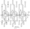
- the second initialization line Vinit2 and the third initialization line Vinit3 are all mesh-shaped, and each pixel 02 includes three sub-pixels 021 (R, G, and B) as shown in FIG. 6
- the first initialization line Vinit1 coupled to only one sub-pixel 021 has the second portion Vinit1-2
- the second initialization line Vinit2 coupled to only one sub-pixel 021 has the second portion Vinit2-2
- the third initialization line Vinit3 coupled to only one sub-pixel 021 has the second portion Vinit3-2.
- each pixel 02 includes three sub-pixels 021 (R, G, and B) as shown in FIG. 6
- the second initialization line Vinit2 coupled to only one sub-pixel 021 has the second portion Vinit2-2
- the third initialization line Vinit3 coupled to only one sub-pixel 021 has the second portion Vinit3-2.
- different sub-pixels 021 are coupled to different initialization lines having the second portion, which can facilitate the wiring in the space, simplify the structure, and save the wiring costs.
- the initialization lines having the second portion coupled to the three sub-pixels 021 are the first initialization line Vinit1, the second initialization line Vinit2 and the third initialization line Vinit3, respectively. That is, it can be considered that the second portion of the first initialization line Vinit1, the second portion of the second initialization line Vinit2 and the second portion of the third initialization line Vinit3 are in one-to-one correspondence with the three sub-pixels 021.
- This design approach is referred to as a simultaneous Vinit1, Vinit2 and Vinit3 mesh design.
- the initialization line having the second portion coupled to the first sub-pixel R is the second initialization line Vinit2
- the initialization line having the second portion coupled to the second sub-pixel G is the third initialization line Vinit3.
- Vinit2 and Vinit3 mesh design there is remaining space in the area where the third sub-pixel B is disposed, and correspondingly, the second power line VSS is disposed near the area where the third sub-pixel B is disposed, to implement the VSS in AA design.
- This design is referred to as: Vinit2 and Vinit3 mesh design, and simultaneous VSS in AA design.
- This implementation is applicable to the large-size, medium-size, wearable or mobile display panels described in the foregoing embodiments.
- the pixel structure in the display panel is the RGB pixel structure shown in FIG. 6 , or the GGRB pixel structure shown in FIG. 7 .
- this implementation is also applicable to other types of display panels as long as the space allows.
- the initialization line coupled to partial sub-pixels 021 of the at least three sub-pixels 021 has the second portion.
- the number of the partial sub-pixels is greater than or equal to 1. That is, for each mesh-shaped initialization line, the initialization line coupled to one or more than two sub-pixels 021 has the second portion. In addition, since the initialization line coupled to partial sub-pixels rather than all sub-pixels 021 has the second portion, the number of the partial sub-pixels is less than the number of the sub-pixels 021 included in each pixel 02.
- each pixel 02 includes three sub-pixels 021 (R, G, and B) shown in FIG. 6
- the second initialization line Vinit2 coupled to two sub-pixels 021 (R and B) has the second portion Vinit2-2
- the third initialization line Vinit3 coupled to only one sub-pixel (G) has the second portion Vinit3-2.
- second initialization line Vinit2 for the second initialization line Vinit2, second initialization line Vinit2 coupled to two sub-pixels 021 has the second portion Vinit2-2; and for the third initialization line Vinit3, the third initialization line Vinit3 coupled to one sub-pixel 021 has the second portion Vinit3-2.
- each pixel 02 includes four sub-pixels 021 (G, G, R, and B) shown in FIG. 7
- the second initialization line Vinit2 coupled to two sub-pixels 021 has the second portion Vinit2-2
- the third initialization lines Vinit3 coupled to two sub-pixels 021 has the second portion Vinit3-2.
- the second initialization line Vinit2 coupled to two sub-pixels 021 has the second portion Vinit2-2; and for the third initialization line Vinit3, the third initialization line Vinit3 coupled to two sub-pixels 021 has the second portion Vinit3-2.
- the partial sub-pixels 021 described in the foregoing embodiments are sub-pixels 021 that are not adjacent in the first direction X1, and two sub-pixels 021 adjacent in the first direction X1 are coupled to different initialization lines having the second portion, which can facilitate the layout and avoid signal crosstalk.
- the second initialization line Vinit2 coupled to the first sub-pixel R and the third sub-pixel B which are not adjacent has the second portion Vinit2-2.
- the initialization lines having the second portion coupled to the first sub-pixel R and second sub-pixel G which are adjacent are the second initialization line Vinit2 and the third initialization line Vinit3, respectively
- the initialization lines having the second portion coupled to the second sub-pixel G and third sub-pixel B which are adjacent are the third initialization line Vinit3 and the second initialization line Vinit2, respectively.
- This design is referred to as Vinit2, Vinit3 and Vinit2 mesh design.
- the third initialization line Vinit3 coupled to the first sub-pixel G and the third sub-pixel R which are not adjacent has the second portion Vinit3-2
- the second initialization line Vinit2 coupled to the second sub-pixel G and the fourth sub-pixel B which are not adjacent has the second portion Vinit2-2.
- the initialization lines having the second portion coupled to the first sub-pixel G and second sub-pixel G which are adjacent are the third initialization line Vinit3 and the second initialization line Vinit2, respectively; the initialization lines having the second portion coupled to the second sub-pixel G and third sub-pixel R which are adjacent are the second initialization line Vinit2 and the third initialization line Vinit3, respectively; and the initialization lines having the second portion coupled to the third sub-pixel R and third sub-pixel B which are adjacent are the third initialization line Vinit3 and the second initialization line Vinit2, respectively.
- This design approach is referred to as Vinit2, Vinit3, Vinit2 and Vinit3 mesh design.
- This implementation is applicable to display panels having the special structure described in the foregoing embodiments, for example, a mobile phone with a hole in the middle of the screen. Certainly, it is also applicable to other types of display panels as long as the space allows.
- the initialization line coupled to each sub-pixel 021 of the at least three sub-pixels 021 has the second portion
- the initialization line coupled to partial sub-pixels 021 of the at least three sub-pixels 021 has the second portion
- the number of the partial sub-pixels 021 is greater than or equal to 1, and the partial sub-pixels 021 are sub-pixels 021 that are not adjacent in the first direction X1.
- each pixel 02 includes four sub-pixels 021 (G, G, R, and B) shown in FIG. 7 as an example
- the third initialization line Vinit3 coupled to the four sub-pixels has the second portion Vinit3-2
- the second initialization line Vinit2 coupled to only two sub-pixels one G and R has the second portion Vinit2-2.
- the third initialization line Vinit3 coupled to each of the four sub-pixels 021 has the second portion Vinit3-2; and for the second initialization line Vinit2, the second initialization line Vinit2 coupled to only two of the four sub-pixels 021 has the second portion Vinit2-2, and the second initialization line Vinit2 coupled to the first sub-pixel G and the third sub-pixel R which are not adjacent has the second portion Vinit2-2.
- This design is referred to as Vinit32, Vinit3, Vinit32 and Vinit3 mesh design.
- This implementation is applicable to display panels having the GGRB pixel structure described in the foregoing embodiments. Certainly, it is also applicable to other types of display panels as long as the space allows.
- the first portion of the first initialization line Vinit1 is marked with Vinit1-1
- the first portion of the second initialization line Vinit2 is marked with Vinit2-1
- the first portion of the third initialization line Vinit3 is marked with Vinit3-1.
- the pixel 02 in the display panel includes a plurality of metal layers sequentially stacked in a direction going away from the substrate 01.
- the pixel circuit P1 in the pixel 02 includes a plurality of metal layers.
- a first portion of each of the signal lines is disposed in the same layer as one metal layer of the plurality of metal layers, and the second portion of each of the signal lines is disposed in the same layer as another metal layer of the plurality of metal layers.
- Each of the other signal lines is disposed in the same layer as any metal layer of the plurality of metal layers.
- the first portion and the second portion are both disposed in the same layer as the same metal layer of the plurality of metal layers.
- being disposed in the same layer refers to that film layers for forming a specific pattern are formed by the same film forming process, and then the film layers are patterned by one patterning process using the same mask to form a layer structure.
- the one patterning process includes multiple exposure, development, or etching processes, and the specific pattern in the formed layer structure is continuous or discontinuous. That is, the plurality of elements, components, structures and/or portions disposed in the same layer are made from the same material, and are formed by the same patterning process. In this way, the manufacturing process can be simplified, the manufacturing cost can be reduced, and the manufacturing efficiency can be increased.
- the plurality of metal layers in the pixel circuit P1 include a first gate metal layer Gate1, a second gate metal layer Gate2, a third gate metal layer Gate3, a first source-drain metal layer SD1 and a second source-drain metal layer SD2 that are sequentially stacked in the direction going away from the substrate 01.
- the second gate metal layer Gate2 and the third gate metal layer Gate3 are used as the gate of the N-type oxide transistor T2, and the first gate metal layer Gate1 is used as the gate of the P-type LTPS transistor T8.
- the first source-drain metal layer SD1 is used as the source and the drain of each transistor.
- the second source-drain metal layer SD2 is coupled to the anode Anode of the light-emitting element L1, and is coupled to the first source-drain metal layer SD1 by an electrical connection line, so as to indirectly lap the first source-drain metal layer SD1 with the anode Anode of the light-emitting element L1.
- the pixel circuit P1 further includes an active layer.
- the active layer of the P-type transistor is marked with Poly, and the active layer of the N-type transistor is marked with IGZO.
- Indium gallium zinc oxide (IGZO) is an oxide material, and certainly, the oxide material is not limited to IGZO.
- the first source-drain metal layer SD1 is lapped with the active layer.
- An insulator layer is provided between every two adjacent film layers to insulate the two film layers from each other, thereby avoiding mutual interference.
- FIG. 14 it includes a first gate insulator (GI) layer GI1 disposed between the active layer Poly and the first gate metal layer Gate1, a second gate insulator layer GI2 disposed between the first gate metal layer Gate 1 and the second gate metal layer Gate2, a third gate insulator layer GI3 disposed between the second gate metal layer Gate2 and the active layer IGZO, a fourth gate insulator layer GI4 disposed between the active layer IGZO and the third gate metal layer Gate3, an interlayer dielectric (ILD) layer disposed between the third gate metal layer Gate3 and the first source-drain metal layer SD1, and a passivation layer (PVX) and a first planarization layer (PLN) PLN1 that are disposed between the first source-drain metal layer SD1 and the second source-drain metal layer SD2 and are sequentially stacked in the direction going away from the substrate 01, and a second planarization layer PLN2 disposed between the second source-drain metal layer SD
- GI gate insul
- the first source-drain metal layer SD1 is coupled to the film layer (e.g., the active layer Poly) that needs to be lapped with through a via hole penetrating through a plurality of film layers; the second source-drain metal layer SD2 is lapped with the first source-drain metal layer SD1 through a via hole penetrating through the first planarization layer PLN1 and the passivation layer PVX; and the anode Anode is lapped with the second source-drain metal layer SD2 through a via hole penetrating through the second planarization layer PLN2.
- the film layer e.g., the active layer Poly
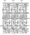
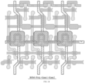
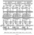
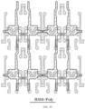
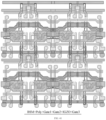
- FIG. 15 shows a partial structural layout of a display panel.
- FIG. 16 shows a partial structural layout of a display panel.
- FIG. 17 shows a structural layout of a display panel.
- FIG. 18 shows a structural layout of a display panel.
- FIG. 19 shows a structural layout of a display panel.
- FIG. 20 to FIG. 32 sequentially show the structural layout of each single layer and the gradually stacked layers.
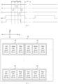
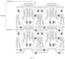
- FIG. 20 includes an base metal BSM and an active layer Poly, and FIG. 20 further schematically marks the positions of the active layers Poly in the P-type transistors except the N-type transistor (i.e., the second transistor T2), including the first transistor T1, the third transistor T3, the fourth transistor T4, the fifth transistor T5, the sixth transistor T6, the seventh transistor T7 and the eighth transistor T8, and also schematically marks the division of the sub-pixels R, G and B.
- the N-type transistor i.e., the second transistor T2
- the N-type transistor i.e., the second transistor T2
- the N-type transistor i.e., the second transistor T2
- the N-type transistor i.e., the second transistor T2
- the N-type transistor i.e., the second transistor T2
- the N-type transistor i.e., the second transistor T2
- the N-type transistor i.e., the second transistor T2
- the N-type transistor i.e., the second transistor T
- the structural layout shown in FIG. 21 includes a first gate metal layer Gate1.
- the structural layout shown in FIG. 22 includes the base metal BSM, the active layer Poly and the first gate metal layer Gate1 which are stacked.
- the structural layout shown in FIG. 23 includes a second gate metal layer Gate2.
- the structural layout shown in FIG. 24 includes the base metal BSM, the active layer Poly, the first gate metal layer Gate1 and the second gate metal layer Gate2 which are stacked.
- the structural layout shown in FIG. 25 includes the active layer IGZO of the N-type transistor, and correspondingly marks the second transistor T2, and the structural layout further includes a third gate metal layer Gate3.
- the structural layout shown in FIG. 26 includes the base metal BSM, the active layer Poly, the first gate metal layer Gate1, the second gate metal layer Gate2, the active layer IGZO and the third gate metal layer Gate3 which are stacked.
- the structural layout shown in FIG. 27 includes an interlayer insulator layer ILD and a first source-drain metal layer SD1.
- the interlayer insulator layer ILD includes an ILD_L and an ILD_O that are configured to penetrate through different film layers to be lapped with different film layers.
- the via hole formed by ILD_L is marked with K1
- the via hole formed by ILD_O is marked with K2.
- FIG. 27 marks all via holes K2, and the remaining via holes which are not marked are via holes K1.
- the structural layout shown in FIG. 28 includes the base metal BSM, the active layer Poly, the first gate metal layer Gate1, the second gate metal layer Gate2, the active layer IGZO, the third gate metal layer Gate3, the interlayer insulator layer ILD, and the first source-drain metal layer SD1 which are stacked.
- the structural layout shown in FIG. 29 includes a first planarization layer PLN1, a second source-drain metal layer SD2 and a second planarization layer PLN2.
- the structural layout shown in FIG. 30 includes the base metal BSM, the active layer Poly, the first gate metal layer Gate1, the second gate metal layer Gate2, the active layer IGZO, the third gate metal layer Gate3, the interlayer insulator layer ILD, the first source-drain metal layer SD1, the first planarization layer PLN1, the second source-drain metal layer SD2 and the second planarization layer PLN2 which are stacked.
- FIG. 31 The structural layout shown in FIG. 31 includes an anode Anode and a pixel defining layer PDL in addition to the first planarization layer PLN1, the second source-drain metal layer SD2 and the second planarization layer PLN2 shown in FIG. 29 .
- FIG. 31 further schematically marks a sub-pixel R, a sub-pixel G and a sub-pixel B.
- the structural layout shown in FIG. 32 includes the base metal BSM, the active layer Poly, the first gate metal layer Gate1, the second gate metal layer Gate2, the active layer IGZO, the third gate metal layer Gate3, the interlayer insulator layer ILD, the first source-drain metal layer SD1, the first planarization layer PLN1, the second source-drain metal layer SD2, the second planarization layer PLN2, the anode Anode and the pixel defining layer PDL which are stacked.
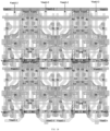
- FIG. 33 to FIG. 50 further sequentially show each single-layer and gradually stacked layers.
- the structural layout shown in FIG. 33 includes a base metal BSM.
- FIG. 34 includes an active layer Poly, and FIG. 34 further schematically marks the positions of the active layers Poly in the P-type transistors except the N-type transistor (i.e., the second transistor T2), including the first transistor T1, the third transistor T3, the fourth transistor T4, the fifth transistor T5, the sixth transistor T6, the seventh transistor T7 and the eighth transistor T8, and also schematically marks the division of the sub-pixel R, the sub-pixel G, the sub-pixel B and the sub-pixel G.
- the N-type transistor i.e., the second transistor T2
- the N-type transistor i.e., the second transistor T2
- the N-type transistor i.e., the second transistor T2
- the N-type transistor i.e., the second transistor T2
- the N-type transistor i.e., the second transistor T2
- the N-type transistor i.e., the second transistor T2
- the N-type transistor i.e., the second transistor T2
- the N-type transistor i.
- the structural layout shown in FIG. 35 includes the base metal BSM and the active layer Poly which are stacked.
- the structural layout shown in FIG. 36 includes a first gate metal layer Gate1.
- the structural layout shown in FIG. 37 includes the base metal BSM, the active layer Poly and the first gate metal layer Gate1 which are stacked.
- the structural layout shown in FIG. 38 includes a second gate metal layer Gate2.
- the structural layout shown in FIG. 39 includes the base metal BSM, the active layer Poly, the first gate metal layer Gate1 and he second gate metal layer Gate2 which are stacked.
- the structural layout shown in FIG. 40 includes the active layer IGZO of the N-type transistor, and correspondingly marks the second transistor T2, and the structural layout further includes a third gate metal layer Gate3.
- the structural layout shown in FIG. 41 includes the base metal BSM, the active layer Poly, the first gate metal layer Gate1, the second gate metal layer Gate2, the active layer IGZO, and the third gate metal layer Gate3 which are stacked.
- the structural layout shown in FIG. 42 includes an interlayer insulator layer ILD in addition to the third gate metal layer Gate3 and the active layer IGZO shown in FIG. 40 .
- the interlayer insulator layer ILD includes an ILD_L and an ILD_O that are configured to penetrate through different film layers to lap with different film layers.
- the via hole formed by ILD_L is marked with K1
- the via hole formed by ILD_O is marked with K2.
- FIG. 42 marks all via holes K2, and the remaining via holes which are not marked are via holes K1.
- the structural layout shown in FIG. 43 includes the base metal BSM, the active layer Poly, the first gate metal layer Gate1, the second gate metal layer Gate2, the active layer IGZO, the third gate metal layer Gate3 and the interlayer insulator layer ILD which are stacked.
- the structural layout shown in FIG. 44 includes a first source-drain metal layer SD1.
- the structural layout shown in FIG. 45 includes the base metal BSM, the active layer Poly, the first gate metal layer Gate1, the second gate metal layer Gate2, the active layer IGZO, the third gate metal layer Gate3, the interlayer insulator layer ILD and the first source-drain metal layer SD1 which are stacked.
- the structural layout shown in FIG. 46 includes a first planarization layer PLN1, a second source-drain metal layer SD2 and a second planarization layer PLN2.
- the structural layout shown in FIG. 47 includes the first source-drain metal layer SD1, the first planarization layer PLN1, the second source-drain metal layer SD2 and the second planarization layer PLN2 which are stacked.
- the structural layout shown in FIG. 48 includes the base metal BSM, the active layer Poly, the first gate metal layer Gate1, the second gate metal layer Gate2, the active layer IGZO, the third gate metal layer Gate3, the interlayer insulator layer ILD, the first source-drain metal layer SD1, the first planarization layer PLN1, the second source-drain metal layer SD2 and the second planarization layer PLN2 which are stacked.
- FIG. 49 includes an anode Anode and a pixel defining layer PDL in addition to the first planarization layer PLN1, the second source-drain metal layer SD2 and the second planarization layer PLN2 shown in FIG. 46 .
- FIG. 48 further schematically shows one sub-pixel R, two sub-pixels G, and one sub-pixel B.
- the structural layout shown in FIG. 50 includes the base metal BSM, the active layer Poly, the first gate metal layer Gate1, the second gate metal layer Gate2, the active layer IGZO, the third gate metal layer Gate3, the interlayer insulator layer ILD, the first source-drain metal layer SD1, the first planarization layer PLN1, the second source-drain metal layer SD2, the second planarization layer PLN 2, the anode Anode and the pixel defining layer PDL which are stacked.
- the mesh-shaped signal lines in the embodiments of the present disclosure include the second initialization line Vinit2 and the third initialization line Vinit3.
- the first portion Vinit2-1 of the second initialization line Vinit2 extends along the first direction X1, and is disposed in the same layer as the first source-drain metal layer SD1.
- the second portion Vinit2-2 of the second initialization line Vinit2 extends along the second direction X2, and is disposed in the same layer as the second source-drain metal layer SD2.
- the first portion Vinit2-1 and the second portion Vinit2-2 of the second initialization line Vinit2 are both disposed in the same layer as the first source-drain metal layer SD1.
- the first portion Vinit3-1 of the third initialization line Vinit3 extends along the first direction X1, and is disposed in the same layer as the third gate metal layer Gate3.
- the second portion Vinit3-2 of the third initialization line Vinit3 extends along the second direction X2, and is disposed in the same layer as the second source-drain metal layer SD2.
- FIG. 29 and FIG. 46 both show a via hole K01 through which the first portion Vinit2-1 and the second portion Vinit2-2 of the second initialization line Vinit2 are connected, and a via hole K02 through which the first portion Vinit3-1 and the second portion Vinit3-2 of the third initialization line Vinit3 are connected.
- the via hole K01 and the via hole K02 penetrate through the first planarization layer PLN1.
- the first initialization line Vinit1 is not mesh-shaped. As can be seen from FIG. 23 and FIG. 38 , the first initialization line Vinit1 extends along the first direction X1, and is disposed in the same layer as the second gate metal layer Gate2.
- the mesh-shaped signal lines further include a second power line VSS disposed in the display region AA of the substrate 01. As can be seen from FIG. 3 and FIG.
- the first portion of the second power line VSS extends along the first direction X1, and is disposed in the same layer as the first source-drain metal layer SD1; and the second portion of the second power line VSS extends along the second direction X2, and is disposed in the same layer as the second source-drain metal layer SD2 (the meshed-shape of the second power line VSS is not shown in the figure).
- the second power line VSS disposed in the display region AA of the substrate 01 is not mesh-shaped.
- the second power line VSS disposed in the display region AA of the substrate 01 extends along the second direction X2, and is disposed in the same layer as the second source-drain metal layer SD2.
- the mesh-shaped signal lines further include the first initialization line Vinit1. As can be seen from FIG. 7 and FIG.
- the first portion Vinit1-1 of the first initialization line Vinit1 extends along the first direction X1, and is disposed in the same layer as the second gate metal layer Gate2; and the second portion Vinit1-2 of the first initialization line Vinit1 extends along the second direction X2, and is disposed in the same layer as the second source-drain metal layer SD2.
- the first initialization line Vinit1 or the second power line VSS disposed in the display region AA of the substrate 01 is mesh-shaped.
- the first initialization line Vinit1 and the second power line VSS disposed in the display region AA of the substrate 01 are both mesh-shaped.
- the mesh-shaped design reference can be made to the foregoing embodiments, and details are not described herein again.
- the light emission control line EM extends along the first direction X1, and is disposed in the same layer as the first gate metal layer Gate1.
- the second gate line G2 extends along the first direction X1, and is disposed in the same layer as the second gate metal layer Gate2 and the third gate metal layer Gate3, respectively.
- the data line D1 extends along the second direction X2, and is disposed in the same layer as the second source-drain metal layer SD2.
- the first power line VDD includes three portions coupled to each other.
- one portion of the first power line VDD extends along the first direction X1, and is disposed in the same layer as the second gate metal layer Gate2.
- another portion of the first power line VDD extends along the second direction X2, and is disposed in the same layer as the first source-drain metal layer SD1.
- the other portion of the first power line VDD extends along the second direction X2, and is disposed in the same layer as the second source-drain metal layer SD2.
- the first reset line R1, the first gate line G1 and the second reset line R2 all extend along the first direction X1, and are disposed in the same layer as the first gate metal layer Gate1.
- the first reset line R1, the first gate line G1 and the second reset line R2 all extend along the first direction X1, and are disposed in the same layer as the first source-drain metal layer SD1. Based on this, it can be seen from FIG. 4 and FIG. 21 that the gate of the transistor (i.e., the fifth transistor T5) coupled to the first reset line R1, the gate of the transistor (i.e., the first transistor T1) coupled to the first gate line G1, and the gate of the transistor (i.e., the sixth transistor T6) coupled to the second reset line R2 are all disposed in the same layer as the first gate metal layer Gate1. Based on this, it can be seen from FIG.
- first gate metal layer Gate1 and the first source-drain metal layer SD1 are lapped with each other to realize the coupling between the gate of the transistor and the corresponding signal line, for example, the reliable coupling between the first gate line G1 and the gate of the first transistor T1. The same is to the coupling between other signal lines and the gate of the transistor, which is not repeated herein.
- the embodiments of the present disclosure provide a display panel.
- the pixel circuit of each sub-pixel includes a drive circuit and a reset circuit.
- the drive circuit can control the potential of the second node based on the potential of the first node and the potential of the third node, and when the second node is connected to the light-emitting element, the potential transmitted by the drive circuit to the second node can drive the light-emitting element to emit light.
- the reset circuit can transmit an initialization signal to the first node, the second node and the light-emitting element, respectively, to reset the first node, the second node and the light-emitting element. In this way, the potentials of the nodes in the pixel circuit can keep consistent, and each pixel circuit can reliably drive the light-emitting element to emit light, thereby solving the brightness difference and ensuring a better display effect.
- At least one of the initialization lines which provide the initialization signals is set to be mesh-shaped, which can improve the stability of the initialization signal provided by the initialization line, thereby further ensuring a better display effect.
- FIG. 51 is a schematic structural diagram of a display device according to some embodiments of the present disclosure. As shown in FIG. 51 , the display device includes a power supply assembly J1 and a display panel M1 as described in the foregoing embodiments.
- the power supply assembly J1 is coupled to the display panel M1, and is configured to supply power to the display panel M1.
- the display device described in the embodiments of the present disclosure includes any product or component having a display function, such as an OLED display device, a mobile phone, a tablet computer, a flexible display device, a television, and a display.
- a display function such as an OLED display device, a mobile phone, a tablet computer, a flexible display device, a television, and a display.
- the terms "first,” and “second” are merely used for descriptive purpose, but cannot be construed as indicating or implying any relative importance.
- the term “a plurality of” refers to two or more, unless specifically defined otherwise.
Landscapes
- Engineering & Computer Science (AREA)
- Microelectronics & Electronic Packaging (AREA)
- Physics & Mathematics (AREA)
- Computer Hardware Design (AREA)
- General Physics & Mathematics (AREA)
- Theoretical Computer Science (AREA)
- Electroluminescent Light Sources (AREA)
- Devices For Indicating Variable Information By Combining Individual Elements (AREA)
- Control Of El Displays (AREA)
- Control Of Indicators Other Than Cathode Ray Tubes (AREA)
Applications Claiming Priority (1)
| Application Number | Priority Date | Filing Date | Title |
|---|---|---|---|
| PCT/CN2023/070523 WO2024145841A1 (zh) | 2023-01-04 | 2023-01-04 | 显示面板及显示装置 |
Publications (2)
| Publication Number | Publication Date |
|---|---|
| EP4567893A1 true EP4567893A1 (de) | 2025-06-11 |
| EP4567893A4 EP4567893A4 (de) | 2025-11-05 |
Family
ID=91803432
Family Applications (1)
| Application Number | Title | Priority Date | Filing Date |
|---|---|---|---|
| EP23914000.7A Pending EP4567893A4 (de) | 2023-01-04 | 2023-01-04 | Anzeigetafel und anzeigevorrichtung |
Country Status (5)
| Country | Link |
|---|---|
| US (1) | US20240431160A1 (de) |
| EP (1) | EP4567893A4 (de) |
| JP (1) | JP2026501462A (de) |
| CN (1) | CN118749136A (de) |
| WO (1) | WO2024145841A1 (de) |
Families Citing this family (2)
| Publication number | Priority date | Publication date | Assignee | Title |
|---|---|---|---|---|
| CN120071851A (zh) * | 2025-03-31 | 2025-05-30 | 惠科股份有限公司 | 栅极驱动电路、制备方法和显示面板 |
| CN120220594A (zh) * | 2025-04-24 | 2025-06-27 | 京东方科技集团股份有限公司 | 像素电路的驱动方法 |
Family Cites Families (12)
| Publication number | Priority date | Publication date | Assignee | Title |
|---|---|---|---|---|
| CN104898887B (zh) * | 2015-06-23 | 2017-10-17 | 京东方科技集团股份有限公司 | 一种内嵌式触摸显示屏、其驱动方法及显示装置 |
| JP2018036290A (ja) * | 2016-08-29 | 2018-03-08 | 株式会社ジャパンディスプレイ | 表示装置 |
| CN111477669B (zh) * | 2020-05-09 | 2023-04-18 | 京东方科技集团股份有限公司 | 一种显示面板及其制作方法、显示装置 |
| GB2614200A (en) * | 2021-04-28 | 2023-06-28 | Boe Technology Group Co Ltd | Display substrate and display panel |
| CN115691411B (zh) * | 2021-07-30 | 2025-04-08 | 京东方科技集团股份有限公司 | 像素电路及其驱动方法、显示装置 |
| CN113707704B (zh) * | 2021-09-02 | 2024-10-18 | 京东方科技集团股份有限公司 | 显示基板和显示装置 |
| US20240177659A1 (en) * | 2021-09-02 | 2024-05-30 | Chengdu Boe Optoelectronics Technology Co., Ltd. | Display substrate and display apparatus |
| CN116347930B (zh) * | 2021-09-23 | 2026-02-03 | 京东方科技集团股份有限公司 | 显示基板和显示装置 |
| CN116018025B (zh) * | 2021-10-20 | 2025-10-28 | 北京京东方技术开发有限公司 | 显示基板及显示装置 |
| CN113793568A (zh) * | 2021-10-27 | 2021-12-14 | Oppo广东移动通信有限公司 | 像素驱动电路及其控制方法、显示屏和显示设备 |
| CN114974130A (zh) * | 2022-05-24 | 2022-08-30 | 京东方科技集团股份有限公司 | 像素驱动电路及其驱动方法、阵列基板及显示装置 |
| CN115394252B (zh) * | 2022-09-20 | 2025-06-17 | 京东方科技集团股份有限公司 | 一种像素驱动电路及其驱动方法、显示面板 |
-
2023
- 2023-01-04 WO PCT/CN2023/070523 patent/WO2024145841A1/zh not_active Ceased
- 2023-01-04 CN CN202380000017.4A patent/CN118749136A/zh active Pending
- 2023-01-04 EP EP23914000.7A patent/EP4567893A4/de active Pending
- 2023-01-04 JP JP2025539965A patent/JP2026501462A/ja active Pending
- 2023-01-04 US US18/289,573 patent/US20240431160A1/en active Pending
Also Published As
| Publication number | Publication date |
|---|---|
| WO2024145841A1 (zh) | 2024-07-11 |
| CN118749136A (zh) | 2024-10-08 |
| EP4567893A4 (de) | 2025-11-05 |
| JP2026501462A (ja) | 2026-01-15 |
| US20240431160A1 (en) | 2024-12-26 |
Similar Documents
| Publication | Publication Date | Title |
|---|---|---|
| CN115398523B (zh) | 像素驱动电路及其驱动方法、显示基板、显示装置 | |
| US10453387B2 (en) | Display panel, display device, pixel driving circuit, and control method for the same | |
| US11568821B2 (en) | Array substrate and method for manufacturing same and method for controlling same, and display apparatus | |
| CN111292687B (zh) | 像素驱动电路、像素结构及显示面板 | |
| JP2023510991A (ja) | 表示パネル及びその製作方法、表示装置 | |
| US12356809B2 (en) | Display substrate and display device | |
| CN106952940A (zh) | 一种有机发光显示面板和有机发光显示装置 | |
| US20250336365A1 (en) | Driving circuit of display panel and display device | |
| EP4567893A1 (de) | Anzeigetafel und anzeigevorrichtung | |
| US12579940B2 (en) | Display substrate and display device | |
| US12236886B2 (en) | Pixel circuit and driving method thereof, display substrate and display device | |
| KR20140127441A (ko) | 박막 트랜지스터 및 유기 발광 표시 장치 | |
| US20240161692A1 (en) | Display panel | |
| US20260007010A1 (en) | Display panel and display device | |
| US20240268172A1 (en) | Display substrate and display device | |
| US12300168B2 (en) | Display panel and display apparatus | |
| CN114667559B (zh) | 像素电路、显示基板和显示装置 | |
| CN114616675B (zh) | 一种显示基板及其制作方法、显示装置 | |
| US20250078755A1 (en) | Display panel and display apparatus | |
| CN117042527A (zh) | 显示基板和显示装置 | |
| CN118678761A (zh) | 显示面板及显示装置 | |
| CN118284925A (zh) | 显示基板及其驱动方法、显示装置 | |
| CN119923678A (zh) | 显示基板和显示装置 | |
| WO2025035446A1 (zh) | 像素驱动电路及其驱动方法、显示装置 | |
| WO2023201609A1 (zh) | 显示面板及其像素电路的驱动方法、显示装置 |
Legal Events
| Date | Code | Title | Description |
|---|---|---|---|
| STAA | Information on the status of an ep patent application or granted ep patent |
Free format text: STATUS: THE INTERNATIONAL PUBLICATION HAS BEEN MADE |
|
| PUAI | Public reference made under article 153(3) epc to a published international application that has entered the european phase |
Free format text: ORIGINAL CODE: 0009012 |
|
| STAA | Information on the status of an ep patent application or granted ep patent |
Free format text: STATUS: REQUEST FOR EXAMINATION WAS MADE |
|
| 17P | Request for examination filed |
Effective date: 20250304 |
|
| AK | Designated contracting states |
Kind code of ref document: A1 Designated state(s): AL AT BE BG CH CY CZ DE DK EE ES FI FR GB GR HR HU IE IS IT LI LT LU LV MC ME MK MT NL NO PL PT RO RS SE SI SK SM TR |
|
| REG | Reference to a national code |
Ref country code: DE Ref legal event code: R079 Free format text: PREVIOUS MAIN CLASS: H01L0027150000 Ipc: G09G0003323300 |
|
| A4 | Supplementary search report drawn up and despatched |
Effective date: 20251007 |
|
| RIC1 | Information provided on ipc code assigned before grant |
Ipc: G09G 3/3233 20160101AFI20250930BHEP Ipc: H10K 59/10 20230101ALN20250930BHEP |
|
| DAV | Request for validation of the european patent (deleted) | ||
| DAX | Request for extension of the european patent (deleted) |