EP4567662A1 - Front-end circuit for an rfid transponder - Google Patents
Front-end circuit for an rfid transponder Download PDFInfo
- Publication number
- EP4567662A1 EP4567662A1 EP23307156.2A EP23307156A EP4567662A1 EP 4567662 A1 EP4567662 A1 EP 4567662A1 EP 23307156 A EP23307156 A EP 23307156A EP 4567662 A1 EP4567662 A1 EP 4567662A1
- Authority
- EP
- European Patent Office
- Prior art keywords
- voltage limiter
- output signal
- voltage
- end circuit
- level
- Prior art date
- Legal status (The legal status is an assumption and is not a legal conclusion. Google has not performed a legal analysis and makes no representation as to the accuracy of the status listed.)
- Pending
Links
Images




Classifications
-
- G—PHYSICS
- G06—COMPUTING OR CALCULATING; COUNTING
- G06K—GRAPHICAL DATA READING; PRESENTATION OF DATA; RECORD CARRIERS; HANDLING RECORD CARRIERS
- G06K19/00—Record carriers for use with machines and with at least a part designed to carry digital markings
- G06K19/06—Record carriers for use with machines and with at least a part designed to carry digital markings characterised by the kind of the digital marking, e.g. shape, nature, code
- G06K19/067—Record carriers with conductive marks, printed circuits or semiconductor circuit elements, e.g. credit or identity cards also with resonating or responding marks without active components
- G06K19/07—Record carriers with conductive marks, printed circuits or semiconductor circuit elements, e.g. credit or identity cards also with resonating or responding marks without active components with integrated circuit chips
- G06K19/0723—Record carriers with conductive marks, printed circuits or semiconductor circuit elements, e.g. credit or identity cards also with resonating or responding marks without active components with integrated circuit chips the record carrier comprising an arrangement for non-contact communication, e.g. wireless communication circuits on transponder cards, non-contact smart cards or RFIDs
-
- G—PHYSICS
- G06—COMPUTING OR CALCULATING; COUNTING
- G06K—GRAPHICAL DATA READING; PRESENTATION OF DATA; RECORD CARRIERS; HANDLING RECORD CARRIERS
- G06K7/00—Methods or arrangements for sensing record carriers, e.g. for reading patterns
- G06K7/01—Details
-
- G—PHYSICS
- G06—COMPUTING OR CALCULATING; COUNTING
- G06K—GRAPHICAL DATA READING; PRESENTATION OF DATA; RECORD CARRIERS; HANDLING RECORD CARRIERS
- G06K19/00—Record carriers for use with machines and with at least a part designed to carry digital markings
- G06K19/06—Record carriers for use with machines and with at least a part designed to carry digital markings characterised by the kind of the digital marking, e.g. shape, nature, code
- G06K19/067—Record carriers with conductive marks, printed circuits or semiconductor circuit elements, e.g. credit or identity cards also with resonating or responding marks without active components
- G06K19/07—Record carriers with conductive marks, printed circuits or semiconductor circuit elements, e.g. credit or identity cards also with resonating or responding marks without active components with integrated circuit chips
- G06K19/0701—Record carriers with conductive marks, printed circuits or semiconductor circuit elements, e.g. credit or identity cards also with resonating or responding marks without active components with integrated circuit chips at least one of the integrated circuit chips comprising an arrangement for power management
-
- G—PHYSICS
- G06—COMPUTING OR CALCULATING; COUNTING
- G06K—GRAPHICAL DATA READING; PRESENTATION OF DATA; RECORD CARRIERS; HANDLING RECORD CARRIERS
- G06K19/00—Record carriers for use with machines and with at least a part designed to carry digital markings
- G06K19/06—Record carriers for use with machines and with at least a part designed to carry digital markings characterised by the kind of the digital marking, e.g. shape, nature, code
- G06K19/067—Record carriers with conductive marks, printed circuits or semiconductor circuit elements, e.g. credit or identity cards also with resonating or responding marks without active components
- G06K19/07—Record carriers with conductive marks, printed circuits or semiconductor circuit elements, e.g. credit or identity cards also with resonating or responding marks without active components with integrated circuit chips
- G06K19/0701—Record carriers with conductive marks, printed circuits or semiconductor circuit elements, e.g. credit or identity cards also with resonating or responding marks without active components with integrated circuit chips at least one of the integrated circuit chips comprising an arrangement for power management
- G06K19/0715—Record carriers with conductive marks, printed circuits or semiconductor circuit elements, e.g. credit or identity cards also with resonating or responding marks without active components with integrated circuit chips at least one of the integrated circuit chips comprising an arrangement for power management the arrangement including means to regulate power transfer to the integrated circuit
-
- H—ELECTRICITY
- H02—GENERATION; CONVERSION OR DISTRIBUTION OF ELECTRIC POWER
- H02M—APPARATUS FOR CONVERSION BETWEEN AC AND AC, BETWEEN AC AND DC, OR BETWEEN DC AND DC, AND FOR USE WITH MAINS OR SIMILAR POWER SUPPLY SYSTEMS; CONVERSION OF DC OR AC INPUT POWER INTO SURGE OUTPUT POWER; CONTROL OR REGULATION THEREOF
- H02M3/00—Conversion of DC power input into DC power output
- H02M3/02—Conversion of DC power input into DC power output without intermediate conversion into AC
- H02M3/04—Conversion of DC power input into DC power output without intermediate conversion into AC by static converters
- H02M3/10—Conversion of DC power input into DC power output without intermediate conversion into AC by static converters using discharge tubes with control electrode or semiconductor devices with control electrode
- H02M3/145—Conversion of DC power input into DC power output without intermediate conversion into AC by static converters using discharge tubes with control electrode or semiconductor devices with control electrode using devices of a triode or transistor type requiring continuous application of a control signal
- H02M3/155—Conversion of DC power input into DC power output without intermediate conversion into AC by static converters using discharge tubes with control electrode or semiconductor devices with control electrode using devices of a triode or transistor type requiring continuous application of a control signal using semiconductor devices only
Definitions
- the present disclosure relates to a front-end circuit for a radio frequency identification (RFID) transponder. Furthermore, the present disclosure relates to a corresponding method of operating a front-end circuit for an RFID transponder.
- RFID radio frequency identification
- RFID transponders may support a feature to intentionally reduce the maximum operating range in response to an RFID reader command, for example, to safeguard privacy. In order to enable this feature, an RFID transponder should determine whether the received power level exceeds a predefined power threshold or not.
- a front-end circuit for an RFID transponder comprising: a rectifier configured to rectify an input voltage received from an antenna; a voltage limiter operatively coupled to the rectifier, said voltage limiter being configured to limit an output voltage of the rectifier; a level detector operatively coupled to the voltage limiter, said level detector being configured to compare a level of an output signal of the voltage limiter with a predefined reference level.
- the level detector is further configured to generate an output signal, wherein said output signal is indicative of a result of comparing the level of the output signal of the voltage limiter with the predefined reference level.
- the level detector and/or the output signal of the voltage limiter are configured to be enabled by a digital control circuit comprised in the RFID transponder.
- the level detector and/or the output signal of the voltage limiter are configured to be enabled during a boot-up of an integrated circuit comprised in the RFID transponder.
- the level detector and/or the output signal of the voltage limiter are configured to be enabled in response to a command received from an external reader device.
- the level detector and/or the output signal of the voltage limiter are permanently enabled.
- the level detector and/or the output signal of the voltage limiter are periodically enabled.
- the output signal of the voltage limiter is a function of a current dissipated by the voltage limiter.
- the output signal of the voltage limiter is a current or a voltage.
- the rectifier, voltage limiter and level detector have configurable circuit parameters.
- an RFID transponder comprises a front-end circuit of the kind set forth, and an integrated circuit operatively coupled to an output of the voltage limiter.
- the integrated circuit is configured to refrain from responding to a command received from an external reader if the level of the output signal of the voltage limiter is below the predefined reference level.
- a method of operating a front-end circuit for an RFID transponder comprising a rectifier, a voltage limiter and a level detector, and the method comprising: rectifying, by the rectifier, an input voltage received from an antenna; limiting, by the voltage limiter, an output voltage of the rectifier; comparing, by the level detector, a level of an output signal of the voltage limiter with a predefined reference level.
- the level detector generates an output signal, wherein said output signal is indicative of a result of comparing the level of the output signal of the voltage limiter with the predefined reference level.
- the output signal of the voltage limiter is a function of a current dissipated by the voltage limiter.
- RFID transponders - which may also be referred to as RFID tags - may support a feature to intentionally reduce the maximum operating range in response to an RFID reader command, for example, to safeguard privacy.
- the optional untraceable command specified in the technical standard "EPC TM Radio-Frequency Identity Protocols Generation-2 UHF RFID Standard", version 2.1, published in July 2018, allows a reader to configure a tag in mode with reduced operating range.
- the reduction of the operating range of a tag may prevent an undesirable tracking of a tag via a long distance to safeguard privacy, while still maintaining an option to read tag data or change the tag configuration at close distance. This may facilitate, for example, the handling of returns of goods in retail application scenarios.
- the operating range R of a tag in the forward-link considering communication from a reader to a tag is depending on the transponder sensitivity P min . R ⁇ 1 / P min
- the sensitivity corresponds to the minimum required power received by the transponder antenna to execute and respond to a reader command.
- a typical reader command for example, requests a tag to read data from a non-volatile memory and to communicate the data back to the reader.
- a transponder can also intentionally reduce the operating range by increasing the effective sensitivity power level P min . This can be achieved by detecting if the received power level exceeds a specific power threshold or not.
- Fig. 1 shows a graph 100 displaying a relationship between the minimum received power and operating frequency for an RFID transponder.
- Fig. 1 illustrates an example of the sensitivity characteristics versus frequency of an RFID transponder for a normal read command response and a command response with a reduced range.
- the sensitivity level is increased by a level ⁇ P min of about 22dBm. This corresponds to a reduction of the operating range from about 16m to about 1.3m considering a maximum equivalent isotropically radiated power (EIRP) transmitter by a reader of 4W.
- EIRP maximum equivalent isotropically radiated power
- RFID tag integrated circuits may implement a feature allowing the tag to be configured in a mode with reduced operating range.
- a tag IC should be able to detect if the received power level exceeds a defined power threshold or not.
- the procedure to check the received power level should be executable in a fast way to not negatively impact the boot-up time of a tag IC.
- the execution of the power check procedure should not cause a change of the absorbed RF power of a tag IC, so as to minimize electromagnetic interference.
- the rectifier 202 rectifies and transforms the RF power received by the transponder antenna to provide a DC voltage at the output VRECT.
- the voltage limiter 204 that is connected to the rectifier output provides a supply voltage at its output VDD for the core circuits of the chip.
- the voltage level at VDD may be substantially identical to the voltage at VRECT.
- the voltage limiter 204 limits the maximum voltage level of VRECT by dissipating the rectifier output current exceeding the current consumption of the transponder core circuits to prevent damage of circuit elements due to overvoltage.
- the front-end circuit 200 uses an additional output signal SENSE of the DC limiter.
- the level of SENSE is a function of the current dissipated by the voltage limiter 204.
- the level of SENSE may be proportional or inversely proportional to the current dissipated by the voltage limiter 204.
- Signal SENSE may be a voltage or a current signal.
- the level detector 206 compares the level of signal SENSE with a reference level at input REF.
- the level detector output OUT indicates to a digital control circuit of the tag IC if signal SENSE has exceeded the reference level at REF or not. This facilitates that the digital control circuit is triggered to limit the operating range of the tag, for example by refraining from responding to a command received from an external reader if the level of the output signal SENSE of the voltage limiter is below the predefined reference level REF.
- the voltage level at VRECT is substantially defined by the voltage limiter 204 at elevated levels of received power.
- the DC power consumption at rectifier output VRECT is in this case proportional to the dissipated current of the voltage limiter 204 assuming that the core current consumption is negligible in relative terms or mostly constant.
- the absorbed RF power at the input of the rectifier 202 is proportional to the DC power consumption at VRECT depending on the power conversion efficiency of the rectifier 202.
- the absorbed input RF power of the rectifier 202 is proportional to the received antenna power as defined by the impedance matching between the antenna and the tag IC.
- the level of SENSE and the threshold defined by REF are proportional to the power received at the antenna.
- the level detector and/or the output signal of the voltage limiter are configured to be enabled by a digital control circuit comprised in the RFID transponder. In this way, the power check may easily be enabled and disabled, for example depending on the application of use case of the RFID transponder.
- the level detector and/or the output signal of the voltage limiter are configured to be enabled during a boot-up of an integrated circuit comprised in the RFID transponder. In this way, the power check may easily be activated, such that it is operational when the RFID transponder is being used.
- the level detector and/or the output signal of the voltage limiter are configured to be enabled in response to a command received from an external reader device. In this way, the power check may only be activated when necessary, such that the power check itself does not consume too much energy.
- the activation of the level detector and/or the output signal of the voltage limiter may be conditional on the setting of configuration bits stored in a non-volatile memory included in the RFID transponder.
- Configuration bits of the non-volatile memory of the RFID transponder to enable, disable, or change the behavior of the level detector and/or the voltage limiter in other ways may be changed in response to a command sent by an external reader device.
- the state of output signal OUT of level detector 206 may be stored temporarily using a digital memory cell for later processing by a digital control circuit included in the RFID transponder.
- a digital control circuit of the RFID transponder may read the state of signal OUT or a state of signal OUT stored in a digital memory cell on the reception of a command from an external reader to decide whether to reply to the reader command or not. In such a way the effective operating range of the RFID transponder may be reduced if the RFID transponder replies only to reader commands if the level of signal SENSE has exceeded a reference level REF, as indicated by output signal OUT of level detector 206.
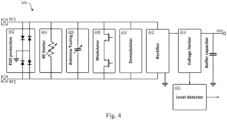
- Fig. 4 shows another illustrative embodiment of a front-end circuit 400 for an RFID transponder.
- the front-end circuit 400 shown in Fig. 4 contains an ESD protection block 402, an RF limiter 404, an antenna tuning block 406, a modulator 408, and a demodulator 410.
- ESD protection block 402 an ESD protection block 402
- RF limiter 404 an RF limiter 404
- antenna tuning block 406 a modulator 408
- demodulator 410 a demodulator 410.
- the power check enabled by the rectifier 412, voltage limiter 414 and level detector 416 may be implemented in a non-limiting example of a typical front-end circuit 400 for an RFID transponder.
- the rectifier 412 rectifies and transforms the received RF voltage from an antenna to provide a DC supply voltage for the chip core circuits (e.g., a digital part and a non-volatile memory).
- the rectifier 412 may typically be implemented by a multi-staged RF charge pump.
- the modulator 408 modulates the input impedance to modulate the signal that is scattered back from the antenna to transmit information to a reader.
- the demodulator 410 demodulates an amplitude modulated signal transmitted by a reader.
- the antenna tuning block 406 tunes the chip input capacitance to maximize the power transfer from the antenna to the chip input.
- the electrostatic discharge (ESD) protection block 402 may typically be implemented by anti-parallel pn-junction diodes.
- the RF limiter 404 limits the RF voltage amplitude at RF1 and RF2 at high received power levels at a connected antenna.
- the voltage limiter 414 limits the output voltage of the rectifier and the core supply voltage. Taken together, the rectifier 412, voltage limiter 414 and level detector 416 implement a check of the received power with reference to a predefined power threshold.
- Fig. 5 shows an illustrative embodiment of a part 500 of a front-end circuit for an RFID transponder.
- Fig. 5 shows a non-limiting example of an implementation of a voltage limiter 502 and a level detector 504 of the kind set forth above.
- the voltage limiter 502 includes a shunt transistor M 1 to dissipate excess current from supply voltage rail VRECT.
- the gate of M 1 is controlled by an amplifier in a closed loop configuration. As VRECT exceeds a reference voltage VREF1 provided to the amplifier, the voltage at the gate of M 1 increases and the drain current of M 1 and thus the input current at terminal VRECT rises.
- the voltage at VRECT approaches a close to constant value due to the increased input current at VRECT and the resulting voltage drop at the finite output resistance of the rectifier (not shown).
- the gate of a second transistor M 2 is connected to the gate terminal of M 1 .
- the resulting drain current of M 2 is proportional to the drain current of M 1 .
- the drain current of Mz causes a voltage drop at Ri that is observable at output SENSE.
- the observable voltage at SENSE is thus inversely proportional to the current dissipated by the voltage limiter.
- the level detector 504 includes a voltage comparator that compares the voltage at input SENSE with a reference voltage VREF2 relative to the voltage level at VRECT denoted as V(VRECT).
- the output signal OUT indicates if the voltage at SENSE has dropped below a voltage equal to V(VRECT) - VREF2 corresponding to a specific level of dissipated current of the voltage limiter.
- the power detection threshold of the power check circuit is defined by reference voltage VREF2, the value of resistor Ri, the ratio of transistor dimensions of M 1 and M 2 , the voltage level of VRECT as defined by reference voltage VREF1, the power conversion efficiency of the rectifier, and the impedance matching between the transponder antenna and the transponder IC.
- a practical transponder IC implementation may provide means to configure these circuit parameters to adjust the power detection threshold.
- a practical implementation of the invention may include switches to switch separate sections of resistor Ri or transistor M 2 to adjust the power detection threshold.
- Fig. 6 shows another illustrative embodiment of a part 600 of a front-end circuit for an RFID transponder.
- Fig. 6 shows another non-limiting example of an implementation of a voltage limiter 602 and a level detector 604 of the kind set forth above.
- the operation of the voltage limiter 602 is similar to the voltage limiter shown in Fig. 5 .
- the gate of transistor M 2 is connected to the gate of transistor M 1 in the same manner as in the circuit of Fig. 5 .
- the output current at terminal SENSE is proportional to the current that is dissipated via transistor M 1 , depending on the ratio of transistor dimensions of M 1 and M 2 .
- the level detector 604 compares the current level at input SENSE with a reference current IREF1.
- Signal SENSE is connected to the input of a current mirror consisting of PMOS transistors M 3 and M 4 .
- the output of the current mirror more specifically the drain of transistor M 4 , is connected to node CMP.
- CMP is furthermore connected to the output of an NMOS current mirror including transistors M 5 and M 6 .
- the input of the NMOS current mirror is connected to a reference current IREF1. If the magnitude of the output current of the PMOS current mirror exceeds the magnitude of the output current of the NMOS current mirror the voltage at CMP rises.
- the voltage at CMP is amplified by a voltage amplifier to a digital signal level at output OUT.
- the power detection threshold of the power check circuit is defined by the ratio of transistor dimensions of M 1 and M 2 , the voltage level of VRECT as defined by reference voltage VREF1, the power conversion efficiency of the rectifier, the impedance matching between the transponder antenna and the transponder IC, the PMOS and NMOS current mirror transistor ratios and the level of the reference current IREF1.
- a practical transponder IC may provide means to configure these circuit parameters to adjust the power detection threshold.
- the reference voltages VREF1, VREF2, the reference current IREF1 or combinations of them as shown in the schematics of Fig. 5 and Fig. 6 may be implemented in a way to achieve a desired temperature behavior to compensate the power detection threshold with respect to temperature drifts of other circuit components or sub-circuits such as the rectifier.
Landscapes
- Engineering & Computer Science (AREA)
- Computer Hardware Design (AREA)
- Microelectronics & Electronic Packaging (AREA)
- Physics & Mathematics (AREA)
- General Physics & Mathematics (AREA)
- Theoretical Computer Science (AREA)
- Computer Networks & Wireless Communication (AREA)
- Power Engineering (AREA)
- Artificial Intelligence (AREA)
- Computer Vision & Pattern Recognition (AREA)
- Near-Field Transmission Systems (AREA)
Abstract
Description
- The present disclosure relates to a front-end circuit for a radio frequency identification (RFID) transponder. Furthermore, the present disclosure relates to a corresponding method of operating a front-end circuit for an RFID transponder.
- RFID transponders may support a feature to intentionally reduce the maximum operating range in response to an RFID reader command, for example, to safeguard privacy. In order to enable this feature, an RFID transponder should determine whether the received power level exceeds a predefined power threshold or not.
- In accordance with a first aspect of the present disclosure, a front-end circuit for an RFID transponder is provided, the front-end circuit comprising: a rectifier configured to rectify an input voltage received from an antenna; a voltage limiter operatively coupled to the rectifier, said voltage limiter being configured to limit an output voltage of the rectifier; a level detector operatively coupled to the voltage limiter, said level detector being configured to compare a level of an output signal of the voltage limiter with a predefined reference level.
- In one or more embodiments, the level detector is further configured to generate an output signal, wherein said output signal is indicative of a result of comparing the level of the output signal of the voltage limiter with the predefined reference level.
- In one or more embodiments, the level detector and/or the output signal of the voltage limiter are configured to be enabled by a digital control circuit comprised in the RFID transponder.
- In one or more embodiments, the level detector and/or the output signal of the voltage limiter are configured to be enabled during a boot-up of an integrated circuit comprised in the RFID transponder.
- In one or more embodiments, the level detector and/or the output signal of the voltage limiter are configured to be enabled in response to a command received from an external reader device.
- In one or more embodiments, the level detector and/or the output signal of the voltage limiter are permanently enabled.
- In one or more embodiments, the level detector and/or the output signal of the voltage limiter are periodically enabled.
- In one or more embodiments, the output signal of the voltage limiter is a function of a current dissipated by the voltage limiter.
- In one or more embodiments, the output signal of the voltage limiter is a current or a voltage.
- In one or more embodiments, the rectifier, voltage limiter and level detector have configurable circuit parameters.
- In one or more embodiments, an RFID transponder comprises a front-end circuit of the kind set forth, and an integrated circuit operatively coupled to an output of the voltage limiter.
- In one or more embodiments, the integrated circuit is configured to refrain from responding to a command received from an external reader if the level of the output signal of the voltage limiter is below the predefined reference level.
- In accordance with a second aspect of the present disclosure, a method of operating a front-end circuit for an RFID transponder is conceived, the front-end circuit comprising a rectifier, a voltage limiter and a level detector, and the method comprising: rectifying, by the rectifier, an input voltage received from an antenna; limiting, by the voltage limiter, an output voltage of the rectifier; comparing, by the level detector, a level of an output signal of the voltage limiter with a predefined reference level.
- In one or more embodiments, the level detector generates an output signal, wherein said output signal is indicative of a result of comparing the level of the output signal of the voltage limiter with the predefined reference level.
- In one or more embodiments, the output signal of the voltage limiter is a function of a current dissipated by the voltage limiter.
- Embodiments will be described in more detail with reference to the appended drawings.
-
Fig. 1 shows a graph displaying a relationship between the minimum received power and operating frequency for an RFID transponder. -
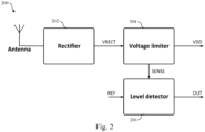
Fig. 2 shows an illustrative embodiment of a front-end circuit for an RFID transponder. -
Fig. 3 shows an illustrative embodiment of a method of operating a front-end circuit. -
Fig. 4 shows another illustrative embodiment of a front-end circuit for an RFID transponder. -
Fig. 5 shows an illustrative embodiment of a part of a front-end circuit for an RFID transponder. -
Fig. 6 shows another illustrative embodiment of a part of a front-end circuit for an RFID transponder. - As mentioned above, RFID transponders - which may also be referred to as RFID tags - may support a feature to intentionally reduce the maximum operating range in response to an RFID reader command, for example, to safeguard privacy. For example, the optional untraceable command specified in the technical standard "EPC™ Radio-Frequency Identity Protocols Generation-2 UHF RFID Standard", version 2.1, published in July 2018, allows a reader to configure a tag in mode with reduced operating range.
- The reduction of the operating range of a tag may prevent an undesirable tracking of a tag via a long distance to safeguard privacy, while still maintaining an option to read tag data or change the tag configuration at close distance. This may facilitate, for example, the handling of returns of goods in retail application scenarios. As shown in equation (1), the operating range R of a tag in the forward-link considering communication from a reader to a tag is depending on the transponder sensitivity Pmin.

- The sensitivity corresponds to the minimum required power received by the transponder antenna to execute and respond to a reader command. A typical reader command, for example, requests a tag to read data from a non-volatile memory and to communicate the data back to the reader. However, a transponder can also intentionally reduce the operating range by increasing the effective sensitivity power level Pmin. This can be achieved by detecting if the received power level exceeds a specific power threshold or not.
-
Fig. 1 shows agraph 100 displaying a relationship between the minimum received power and operating frequency for an RFID transponder. In particular,Fig. 1 illustrates an example of the sensitivity characteristics versus frequency of an RFID transponder for a normal read command response and a command response with a reduced range. The sensitivity level is increased by a level ΔPmin of about 22dBm. This corresponds to a reduction of the operating range from about 16m to about 1.3m considering a maximum equivalent isotropically radiated power (EIRP) transmitter by a reader of 4W. - Thus, RFID tag integrated circuits (ICs) may implement a feature allowing the tag to be configured in a mode with reduced operating range. In order to implement this mode, a tag IC should be able to detect if the received power level exceeds a defined power threshold or not. However, the procedure to check the received power level should be executable in a fast way to not negatively impact the boot-up time of a tag IC. Furthermore, the execution of the power check procedure should not cause a change of the absorbed RF power of a tag IC, so as to minimize electromagnetic interference.
- Now discussed are a front-end circuit for an RFID transponder and a corresponding method of operating a front-end circuit, which facilitate implementing a reduced operating range mode of the RFID transponder, while mitigating negative impacts on its performance.
-
Fig. 2 shows an illustrative embodiment of a front-end circuit 200 for an RFID transponder. The front-end circuit 200 comprises arectifier 202, avoltage limiter 204 which is operatively coupled to therectifier 202, and alevel detector 206 which is operatively coupled to thevoltage limiter 204. Therectifier 202 is configured to rectify an input voltage received from an antenna. It is noted that the antenna is external to the front-end circuit 200. In particular, the antenna may form a part of an RFID transponder into which the front-end circuit 200 may be integrated. Furthermore, thevoltage limiter 204 is configured to limit an output voltage of therectifier 202. Furthermore, thelevel detector 206 is configured to compare a level of an output signal of thevoltage limiter 204 with a predefined reference level. The front-end circuit 200 facilitates implementing a reduced operating range mode of an RFID transponder in which it is integrated, while mitigating negative impacts on the performance of said transponder. In particular, front-end circuit 200 facilitates implementing a power check for an RFID transponder, which utilizes typical rectifier and voltage limiter circuits of an RFID transponder in combination with an additional level detector, thereby enabling circuit implementations with low layout area overhead and current consumption. Furthermore, the internal power consumption and the absorbed RF power of a transponder IC remain largely unchanged at the activation and during the operation of the front-end circuit 200. The execution of the power check therefore requires no time overhead concerning the settling of internal supply voltages and causes no electromagnetic interference due to variation of the absorbed power level. - In a specific implementation of the front-
end circuit 200, therectifier 202 rectifies and transforms the RF power received by the transponder antenna to provide a DC voltage at the output VRECT. Thevoltage limiter 204 that is connected to the rectifier output provides a supply voltage at its output VDD for the core circuits of the chip. In some transponder IC implementations, the voltage level at VDD may be substantially identical to the voltage at VRECT. Thevoltage limiter 204 limits the maximum voltage level of VRECT by dissipating the rectifier output current exceeding the current consumption of the transponder core circuits to prevent damage of circuit elements due to overvoltage. The front-end circuit 200 uses an additional output signal SENSE of the DC limiter. The level of SENSE is a function of the current dissipated by thevoltage limiter 204. For example, the level of SENSE may be proportional or inversely proportional to the current dissipated by thevoltage limiter 204. Signal SENSE may be a voltage or a current signal. - In accordance with the present disclosure, the
level detector 206 compares the level of signal SENSE with a reference level at input REF. In a practical implementation, the level detector output OUT indicates to a digital control circuit of the tag IC if signal SENSE has exceeded the reference level at REF or not. This facilitates that the digital control circuit is triggered to limit the operating range of the tag, for example by refraining from responding to a command received from an external reader if the level of the output signal SENSE of the voltage limiter is below the predefined reference level REF. - It is noted that the voltage level at VRECT is substantially defined by the
voltage limiter 204 at elevated levels of received power. The DC power consumption at rectifier output VRECT is in this case proportional to the dissipated current of thevoltage limiter 204 assuming that the core current consumption is negligible in relative terms or mostly constant. The absorbed RF power at the input of therectifier 202 is proportional to the DC power consumption at VRECT depending on the power conversion efficiency of therectifier 202. Furthermore, the absorbed input RF power of therectifier 202 is proportional to the received antenna power as defined by the impedance matching between the antenna and the tag IC. Thus, the level of SENSE and the threshold defined by REF are proportional to the power received at the antenna. - In one or more embodiments, the level detector and/or the output signal of the voltage limiter are configured to be enabled by a digital control circuit comprised in the RFID transponder. In this way, the power check may easily be enabled and disabled, for example depending on the application of use case of the RFID transponder. In one or more embodiments, the level detector and/or the output signal of the voltage limiter are configured to be enabled during a boot-up of an integrated circuit comprised in the RFID transponder. In this way, the power check may easily be activated, such that it is operational when the RFID transponder is being used. Furthermore, in one or more embodiments, the level detector and/or the output signal of the voltage limiter are configured to be enabled in response to a command received from an external reader device. In this way, the power check may only be activated when necessary, such that the power check itself does not consume too much energy.
- In one or more embodiments, the level detector and/or the output signal of the voltage limiter are permanently enabled. In this way, the level of received power is permanently monitored. In one or more embodiments, the level detector and/or the output signal of the voltage limiter are periodically enabled. In this way, the power check may be activated regularly, while the power check itself does not consume too much energy.
- The activation of the level detector and/or the output signal of the voltage limiter may be conditional on the setting of configuration bits stored in a non-volatile memory included in the RFID transponder. Configuration bits of the non-volatile memory of the RFID transponder to enable, disable, or change the behavior of the level detector and/or the voltage limiter in other ways may be changed in response to a command sent by an external reader device.
- The state of output signal OUT of
level detector 206 may be stored temporarily using a digital memory cell for later processing by a digital control circuit included in the RFID transponder. A digital control circuit of the RFID transponder may read the state of signal OUT or a state of signal OUT stored in a digital memory cell on the reception of a command from an external reader to decide whether to reply to the reader command or not. In such a way the effective operating range of the RFID transponder may be reduced if the RFID transponder replies only to reader commands if the level of signal SENSE has exceeded a reference level REF, as indicated by output signal OUT oflevel detector 206. -
Fig. 3 shows an illustrative embodiment of amethod 300 of operating a front-end circuit. Themethod 300 comprises the following steps. At 302, a rectifier of the front-end circuit rectifies an input voltage received from an antenna. At 304, a voltage limiter of the front-end circuit limits an output voltage of the rectifier. Furthermore, at 306, a level detector of the front-end circuit compares a level of an output signal of the voltage limiter with a predefined reference level. As explained with reference to the corresponding front-end circuit shown inFig. 2 , themethod 300 facilitates implementing a reduced operating range mode of an RFID transponder in which the front-end circuit is integrated, while mitigating negative impacts on the performance of said transponder. -
Fig. 4 shows another illustrative embodiment of a front-end circuit 400 for an RFID transponder. In addition to therectifier 412,voltage limiter 414 andlevel detector 416 of the front-end circuit shown inFig. 2 , the front-end circuit 400 shown inFig. 4 contains an ESD protection block 402, anRF limiter 404, an antenna tuning block 406, amodulator 408, and ademodulator 410. In particular, it is shown how the power check enabled by therectifier 412,voltage limiter 414 andlevel detector 416, may be implemented in a non-limiting example of a typical front-end circuit 400 for an RFID transponder. - In operation, the
rectifier 412 rectifies and transforms the received RF voltage from an antenna to provide a DC supply voltage for the chip core circuits (e.g., a digital part and a non-volatile memory). Therectifier 412 may typically be implemented by a multi-staged RF charge pump. Themodulator 408 modulates the input impedance to modulate the signal that is scattered back from the antenna to transmit information to a reader. Furthermore, thedemodulator 410 demodulates an amplitude modulated signal transmitted by a reader. The antenna tuning block 406 tunes the chip input capacitance to maximize the power transfer from the antenna to the chip input. The electrostatic discharge (ESD) protection block 402 may typically be implemented by anti-parallel pn-junction diodes. Furthermore, theRF limiter 404 limits the RF voltage amplitude at RF1 and RF2 at high received power levels at a connected antenna. Thevoltage limiter 414 limits the output voltage of the rectifier and the core supply voltage. Taken together, therectifier 412,voltage limiter 414 andlevel detector 416 implement a check of the received power with reference to a predefined power threshold. -
Fig. 5 shows an illustrative embodiment of apart 500 of a front-end circuit for an RFID transponder. In particular,Fig. 5 shows a non-limiting example of an implementation of avoltage limiter 502 and alevel detector 504 of the kind set forth above. Thevoltage limiter 502 includes a shunt transistor M1 to dissipate excess current from supply voltage rail VRECT. The gate of M1 is controlled by an amplifier in a closed loop configuration. As VRECT exceeds a reference voltage VREF1 provided to the amplifier, the voltage at the gate of M1 increases and the drain current of M1 and thus the input current at terminal VRECT rises. As a consequence, the voltage at VRECT approaches a close to constant value due to the increased input current at VRECT and the resulting voltage drop at the finite output resistance of the rectifier (not shown). The gate of a second transistor M2 is connected to the gate terminal of M1. The resulting drain current of M2 is proportional to the drain current of M1. The drain current of Mz causes a voltage drop at Ri that is observable at output SENSE. The observable voltage at SENSE is thus inversely proportional to the current dissipated by the voltage limiter. - The
level detector 504 includes a voltage comparator that compares the voltage at input SENSE with a reference voltage VREF2 relative to the voltage level at VRECT denoted as V(VRECT). The output signal OUT indicates if the voltage at SENSE has dropped below a voltage equal to V(VRECT) - VREF2 corresponding to a specific level of dissipated current of the voltage limiter. In this example, the power detection threshold of the power check circuit is defined by reference voltage VREF2, the value of resistor Ri, the ratio of transistor dimensions of M1 and M2, the voltage level of VRECT as defined by reference voltage VREF1, the power conversion efficiency of the rectifier, and the impedance matching between the transponder antenna and the transponder IC. A practical transponder IC implementation may provide means to configure these circuit parameters to adjust the power detection threshold. For example, a practical implementation of the invention may include switches to switch separate sections of resistor Ri or transistor M2 to adjust the power detection threshold. -
Fig. 6 shows another illustrative embodiment of apart 600 of a front-end circuit for an RFID transponder. In particular,Fig. 6 shows another non-limiting example of an implementation of avoltage limiter 602 and alevel detector 604 of the kind set forth above. It is noted that the operation of thevoltage limiter 602 is similar to the voltage limiter shown inFig. 5 . The gate of transistor M2 is connected to the gate of transistor M1 in the same manner as in the circuit ofFig. 5 . As a result, the output current at terminal SENSE is proportional to the current that is dissipated via transistor M1, depending on the ratio of transistor dimensions of M1 and M2. - The
level detector 604 compares the current level at input SENSE with a reference current IREF1. Signal SENSE is connected to the input of a current mirror consisting of PMOS transistors M3 and M4. The output of the current mirror, more specifically the drain of transistor M4, is connected to node CMP. CMP is furthermore connected to the output of an NMOS current mirror including transistors M5 and M6. The input of the NMOS current mirror is connected to a reference current IREF1. If the magnitude of the output current of the PMOS current mirror exceeds the magnitude of the output current of the NMOS current mirror the voltage at CMP rises. The voltage at CMP is amplified by a voltage amplifier to a digital signal level at output OUT. In this example, the power detection threshold of the power check circuit is defined by the ratio of transistor dimensions of M1 and M2, the voltage level of VRECT as defined by reference voltage VREF1, the power conversion efficiency of the rectifier, the impedance matching between the transponder antenna and the transponder IC, the PMOS and NMOS current mirror transistor ratios and the level of the reference current IREF1. A practical transponder IC may provide means to configure these circuit parameters to adjust the power detection threshold. - It is noted that the reference voltages VREF1, VREF2, the reference current IREF1 or combinations of them as shown in the schematics of
Fig. 5 andFig. 6 may be implemented in a way to achieve a desired temperature behavior to compensate the power detection threshold with respect to temperature drifts of other circuit components or sub-circuits such as the rectifier. - Furthermore, it is noted that the embodiments above have been described with reference to different subject-matters. In particular, some embodiments may have been described with reference to method-type claims whereas other embodiments may have been described with reference to apparatus-type claims. However, a person skilled in the art will gather from the above that, unless otherwise indicated, in addition to any combination of features belonging to one type of subject-matter also any combination of features relating to different subject-matters, in particular a combination of features of the method-type claims and features of the apparatus-type claims, is considered to be disclosed with this document.
- Furthermore, it is noted that the drawings are schematic. In different drawings, similar or identical elements are provided with the same reference signs. Furthermore, it is noted that in an effort to provide a concise description of the illustrative embodiments, implementation details which fall into the customary practice of the skilled person may not have been described. It should be appreciated that in the development of any such implementation, as in any engineering or design project, numerous implementation-specific decisions must be made in order to achieve the developers' specific goals, such as compliance with system-related and business-related constraints, which may vary from one implementation to another. Moreover, it should be appreciated that such a development effort might be complex and time consuming, but would nevertheless be a routine undertaking of design, fabrication, and manufacture for those of ordinary skill.
- Finally, it is noted that the skilled person will be able to design many alternative embodiments without departing from the scope of the appended claims. In the claims, any reference sign placed between parentheses shall not be construed as limiting the claim. The word "comprise(s)" or "comprising" does not exclude the presence of elements or steps other than those listed in a claim. The word "a" or "an" preceding an element does not exclude the presence of a plurality of such elements. Measures recited in the claims may be implemented by means of hardware comprising several distinct elements and/or by means of a suitably programmed processor. In a device claim enumerating several means, several of these means may be embodied by one and the same item of hardware. The mere fact that certain measures are recited in mutually different dependent claims does not indicate that a combination of these measures cannot be used to advantage.
-
- 100
- minimum received power versus frequency
- 200
- front-end circuit
- 202
- rectifier
- 204
- voltage limiter
- 206
- level detector
- 300
- method of operating a front-end circuit
- 302
- rectifying, by a rectifier of a front-end circuit, an input voltage received from an antenna
- 304
- limiting, by a voltage limiter of the front-end circuit, an output voltage of the rectifier
- 306
- comparing, by a level detector of the front-end circuit, a level of an output signal of the voltage limiter with a predefined reference level
- 400
- front-end circuit
- 402
- ESD protection
- 404
- RF limiter
- 406
- antenna tuning
- 408
- modulator
- 410
- demodulator
- 412
- rectifier
- 414
- voltage limiter
- 416
- level detector
- 500
- part of a front-end circuit
- 502
- voltage limiter
- 504
- level detector
- 600
- part of a front-end circuit
- 602
- voltage limiter
- 604
- level detector
Claims (15)
- A front-end circuit for a radio frequency identification, RFID, transponder, the front-end circuit comprising:a rectifier configured to rectify an input voltage received from an antenna;a voltage limiter operatively coupled to the rectifier, said voltage limiter being configured to limit an output voltage of the rectifier;a level detector operatively coupled to the voltage limiter, said level detector being configured to compare a level of an output signal of the voltage limiter with a predefined reference level.
- The front-end circuit of claim 1, wherein the level detector is further configured to generate an output signal, wherein said output signal is indicative of a result of comparing the level of the output signal of the voltage limiter with the predefined reference level.
- The front-end circuit of claim 1 or 2, wherein the level detector and/or the output signal of the voltage limiter are configured to be enabled by a digital control circuit comprised in the RFID transponder.
- The front-end circuit of claim 3, wherein the level detector and/or the output signal of the voltage limiter are configured to be enabled during a boot-up of an integrated circuit comprised in the RFID transponder.
- The front-end circuit of claim 3, wherein the level detector and/or the output signal of the voltage limiter are configured to be enabled in response to a command received from an external reader device.
- The front-end circuit of claim 1 or 2, wherein the level detector and/or the output signal of the voltage limiter are permanently enabled.
- The front-end circuit of claim 1 or 2, wherein the level detector and/or the output signal of the voltage limiter are periodically enabled.
- The front-end circuit of any preceding claim, wherein the output signal of the voltage limiter is a function of a current dissipated by the voltage limiter.
- The front-end circuit of any preceding claim, wherein the output signal of the voltage limiter is a current or a voltage.
- The front-end circuit of any preceding claim, wherein the rectifier, voltage limiter and level detector have configurable circuit parameters.
- An RFID transponder comprising the front-end circuit of any preceding claim and an integrated circuit operatively coupled to an output of the voltage limiter.
- The RFID transponder of claim 11, wherein the integrated circuit is configured to refrain from responding to a command received from an external reader if the level of the output signal of the voltage limiter is below the predefined reference level.
- A method of operating a front-end circuit for a radio frequency identification, RFID, transponder, the front-end circuit comprising a rectifier, a voltage limiter and a level detector, and the method comprising:rectifying, by the rectifier, an input voltage received from an antenna;limiting, by the voltage limiter, an output voltage of the rectifier;comparing, by the level detector, a level of an output signal of the voltage limiter with a predefined reference level.
- The method of claim 13, wherein the level detector generates an output signal, wherein said output signal is indicative of a result of comparing the level of the output signal of the voltage limiter with the predefined reference level.
- The method of claim 13 or 14, wherein the output signal of the voltage limiter is a function of a current dissipated by the voltage limiter.
Priority Applications (3)
| Application Number | Priority Date | Filing Date | Title |
|---|---|---|---|
| EP23307156.2A EP4567662A1 (en) | 2023-12-08 | 2023-12-08 | Front-end circuit for an rfid transponder |
| US18/938,908 US20250190736A1 (en) | 2023-12-08 | 2024-11-06 | Front-end circuit for an rfid transponder |
| CN202411777588.1A CN120124648A (en) | 2023-12-08 | 2024-12-05 | Front-end circuit for RFID transponder |
Applications Claiming Priority (1)
| Application Number | Priority Date | Filing Date | Title |
|---|---|---|---|
| EP23307156.2A EP4567662A1 (en) | 2023-12-08 | 2023-12-08 | Front-end circuit for an rfid transponder |
Publications (1)
| Publication Number | Publication Date |
|---|---|
| EP4567662A1 true EP4567662A1 (en) | 2025-06-11 |
Family
ID=89385910
Family Applications (1)
| Application Number | Title | Priority Date | Filing Date |
|---|---|---|---|
| EP23307156.2A Pending EP4567662A1 (en) | 2023-12-08 | 2023-12-08 | Front-end circuit for an rfid transponder |
Country Status (3)
| Country | Link |
|---|---|
| US (1) | US20250190736A1 (en) |
| EP (1) | EP4567662A1 (en) |
| CN (1) | CN120124648A (en) |
Citations (3)
| Publication number | Priority date | Publication date | Assignee | Title |
|---|---|---|---|---|
| EP2963587A1 (en) * | 2014-07-04 | 2016-01-06 | Nxp B.V. | Voltage converter |
| EP3336773A2 (en) * | 2016-12-15 | 2018-06-20 | EM Microelectronic-Marin SA | Voltage regulation circuit for a rfid circuit |
| US20210248331A1 (en) * | 2020-02-10 | 2021-08-12 | Nxp B.V. | Agile time-continuous memory operation for a radio frequency identification transponder |
Family Cites Families (3)
| Publication number | Priority date | Publication date | Assignee | Title |
|---|---|---|---|---|
| JP2006031085A (en) * | 2004-07-12 | 2006-02-02 | Nec Electronics Corp | Semiconductor device for passive rfid, ic tag, and control method therefor |
| DE102007040855B4 (en) * | 2007-08-29 | 2018-01-11 | Texas Instruments Deutschland Gmbh | Transponder backscatter modulator with controlled modulation depth |
| CN103699929B (en) * | 2014-01-08 | 2017-01-04 | 卓捷创芯科技(深圳)有限公司 | The rectification that a kind of switching signal controls and amplitude limiter circuit and passive RF label |
-
2023
- 2023-12-08 EP EP23307156.2A patent/EP4567662A1/en active Pending
-
2024
- 2024-11-06 US US18/938,908 patent/US20250190736A1/en active Pending
- 2024-12-05 CN CN202411777588.1A patent/CN120124648A/en active Pending
Patent Citations (3)
| Publication number | Priority date | Publication date | Assignee | Title |
|---|---|---|---|---|
| EP2963587A1 (en) * | 2014-07-04 | 2016-01-06 | Nxp B.V. | Voltage converter |
| EP3336773A2 (en) * | 2016-12-15 | 2018-06-20 | EM Microelectronic-Marin SA | Voltage regulation circuit for a rfid circuit |
| US20210248331A1 (en) * | 2020-02-10 | 2021-08-12 | Nxp B.V. | Agile time-continuous memory operation for a radio frequency identification transponder |
Also Published As
| Publication number | Publication date |
|---|---|
| CN120124648A (en) | 2025-06-10 |
| US20250190736A1 (en) | 2025-06-12 |
Similar Documents
| Publication | Publication Date | Title |
|---|---|---|
| US8138893B2 (en) | Semiconductor integrated circuit device | |
| US10554261B2 (en) | Card detection device having a magnetic field monitor, system including the device, and method of operating the device | |
| US10333354B2 (en) | Contactless communication medium and electronic device using the same | |
| CA2691828C (en) | Backscatter limited tags | |
| US7990249B1 (en) | RFID tag circuits tags and methods for backscattering with controllable admittance | |
| US8836512B2 (en) | Self tuning RFID | |
| EP2341603A1 (en) | Charge pump stage of radio-frequency identification transponder | |
| JP2005063278A (en) | Non-contact IC card | |
| US5874829A (en) | Supply voltage processing circuit and a data carrier with a supply voltage processing unit | |
| JP6384193B2 (en) | Wireless tag, wireless communication circuit, and degradation detection method | |
| US11580315B2 (en) | Agile time-continuous memory operation for a radio frequency identification transponder | |
| US8292185B2 (en) | Circuits for preventing overvoltage conditions on antenna terminals and method | |
| US6799015B1 (en) | Electromagnetic transponder with a frequency detuning | |
| US20250190736A1 (en) | Front-end circuit for an rfid transponder | |
| US20050200458A1 (en) | Reference circuit enhancement for passive RFID tags | |
| US20070139198A1 (en) | RFID tag capable of limiting over-voltage and method for controlling over-voltage thereof | |
| EP4560527B1 (en) | Radio frequency voltage limiter for an rfid transponder | |
| KR101031414B1 (en) | RFID device | |
| JP6529919B2 (en) | Wireless transmission apparatus and method | |
| KR100874983B1 (en) | Tag chip and its driving method | |
| EP3742341B1 (en) | Rfid transponder and method of operating the same | |
| EP1508871B1 (en) | Data communication device | |
| KR101939239B1 (en) | Envelop Detector for RF Communication | |
| KR101150523B1 (en) | RFID device | |
| KR20110012662A (en) | RFID tag with dual antenna |
Legal Events
| Date | Code | Title | Description |
|---|---|---|---|
| PUAI | Public reference made under article 153(3) epc to a published international application that has entered the european phase |
Free format text: ORIGINAL CODE: 0009012 |
|
| STAA | Information on the status of an ep patent application or granted ep patent |
Free format text: STATUS: THE APPLICATION HAS BEEN PUBLISHED |
|
| AK | Designated contracting states |
Kind code of ref document: A1 Designated state(s): AL AT BE BG CH CY CZ DE DK EE ES FI FR GB GR HR HU IE IS IT LI LT LU LV MC ME MK MT NL NO PL PT RO RS SE SI SK SM TR |
|
| STAA | Information on the status of an ep patent application or granted ep patent |
Free format text: STATUS: REQUEST FOR EXAMINATION WAS MADE |
|
| 17P | Request for examination filed |
Effective date: 20251211 |
|
| GRAP | Despatch of communication of intention to grant a patent |
Free format text: ORIGINAL CODE: EPIDOSNIGR1 |
|
| STAA | Information on the status of an ep patent application or granted ep patent |
Free format text: STATUS: GRANT OF PATENT IS INTENDED |
|
| INTG | Intention to grant announced |
Effective date: 20260608 |
|
| GRAS | Grant fee paid |
Free format text: ORIGINAL CODE: EPIDOSNIGR3 |
|
| GRAA | (expected) grant |
Free format text: ORIGINAL CODE: 0009210 |
|
| STAA | Information on the status of an ep patent application or granted ep patent |
Free format text: STATUS: THE PATENT HAS BEEN GRANTED |