EP4564609A1 - Frequency selective surface and spatial filtering method - Google Patents
Frequency selective surface and spatial filtering method Download PDFInfo
- Publication number
- EP4564609A1 EP4564609A1 EP23856370.4A EP23856370A EP4564609A1 EP 4564609 A1 EP4564609 A1 EP 4564609A1 EP 23856370 A EP23856370 A EP 23856370A EP 4564609 A1 EP4564609 A1 EP 4564609A1
- Authority
- EP
- European Patent Office
- Prior art keywords
- frequency selective
- metal strips
- selective surface
- strip
- metal
- Prior art date
- Legal status (The legal status is an assumption and is not a legal conclusion. Google has not performed a legal analysis and makes no representation as to the accuracy of the status listed.)
- Pending
Links
Images




Classifications
-
- H—ELECTRICITY
- H01—ELECTRIC ELEMENTS
- H01Q—ANTENNAS, i.e. RADIO AERIALS
- H01Q15/00—Devices for reflection, refraction, diffraction or polarisation of waves radiated from an antenna, e.g. quasi-optical devices
- H01Q15/0006—Devices acting selectively as reflecting surface, as diffracting or as refracting device, e.g. frequency filtering or angular spatial filtering devices
- H01Q15/0013—Devices acting selectively as reflecting surface, as diffracting or as refracting device, e.g. frequency filtering or angular spatial filtering devices said selective devices working as frequency-selective reflecting surfaces, e.g. FSS, dichroic plates, surfaces being partly transmissive and reflective
- H01Q15/0026—Devices acting selectively as reflecting surface, as diffracting or as refracting device, e.g. frequency filtering or angular spatial filtering devices said selective devices working as frequency-selective reflecting surfaces, e.g. FSS, dichroic plates, surfaces being partly transmissive and reflective said selective devices having a stacked geometry or having multiple layers
-
- H—ELECTRICITY
- H01—ELECTRIC ELEMENTS
- H01Q—ANTENNAS, i.e. RADIO AERIALS
- H01Q15/00—Devices for reflection, refraction, diffraction or polarisation of waves radiated from an antenna, e.g. quasi-optical devices
- H01Q15/0006—Devices acting selectively as reflecting surface, as diffracting or as refracting device, e.g. frequency filtering or angular spatial filtering devices
- H01Q15/0013—Devices acting selectively as reflecting surface, as diffracting or as refracting device, e.g. frequency filtering or angular spatial filtering devices said selective devices working as frequency-selective reflecting surfaces, e.g. FSS, dichroic plates, surfaces being partly transmissive and reflective
-
- H—ELECTRICITY
- H01—ELECTRIC ELEMENTS
- H01Q—ANTENNAS, i.e. RADIO AERIALS
- H01Q1/00—Details of, or arrangements associated with, antennas
- H01Q1/12—Supports; Mounting means
- H01Q1/22—Supports; Mounting means by structural association with other equipment or articles
- H01Q1/24—Supports; Mounting means by structural association with other equipment or articles with receiving set
- H01Q1/241—Supports; Mounting means by structural association with other equipment or articles with receiving set used in mobile communications, e.g. GSM
- H01Q1/246—Supports; Mounting means by structural association with other equipment or articles with receiving set used in mobile communications, e.g. GSM specially adapted for base stations
Definitions
- Embodiments of the present disclosure relate to the field of communications, and in particular, to a frequency selective surface and a spatial filtering method.
- a 5G active antenna surface faces three major challenges: 1. a new site cannot be added; 2. a 5G active antenna surface cannot be additionally deployed at an existing site deployed with a 4G passive antenna surface; and 3. a 5G active antenna surface can be additionally deployed at an existing site, but the limited height constraints optimal signal coverage.
- a 4G passive antenna surface and 5G active antenna surface integration scheme i.e. an A+P (Active plus Passive, A+P) antenna.
- the A+P antenna is a multi-frequency shared-aperture antenna that uses an integrated interleaving scheme to embed the 5G active antenna surface into the back of the 4G passive antenna surface, so as to achieve integrated deployment.
- the A+P antenna may be aligned with existing networks in performance, and supports separate maintenance and independent deployment of an active antenna surface and a passive antenna surface, thereby greatly reducing operation costs and satisfying the requirements of smooth device upgrade.
- a frequency selective surface In order to meet the A+P antenna performance, a frequency selective surface (FSS) needs to be designed to implement perfect integration of a passive antenna surface and an active antenna surface.
- FSS frequency selective surface
- Embodiments of the present disclosure provide a frequency selective surface and a spatial filtering method, so as to at least solve the problem in the related art that a 4G passive antenna surface cannot be perfectly integrated with a 5G active antenna surface.
- a frequency selective surface unit comprising: a first surface, composed of a plurality of first metal strips interleaved with one another; a second surface, composed of a plurality of second metal strips, wherein each of the second metal strips is provided with a second inter-strip gap, and metal strips at two sides of the second inter-strip gap are connected by means of a metal strip line, so as to form a parallel resonant LC circuit in an H frequency band; and a support plate, the first surface and the second surface being fixed on the same surface or front and back surfaces of the support plate.
- a frequency selective surface is further provided, which is formed by periodic extension of the described frequency selective surface unit.
- a spatial filtering method is further provided.
- the spatial filtering method is implemented using the described frequency selective surface, and comprises: L values or C values of a series resonant LC circuit and a parallel resonant LC circuit are adjusted, so as to control a transmission frequency band and a reflection frequency band of the frequency selective surface unit.
- An A+P antenna is a multi-frequency shared-aperture antenna that uses an integrated interleaving scheme to embed a 5G active antenna surface into the back of a 4G passive antenna surface, so as to achieve integrated deployment.
- the A+P antenna may be aligned with existing networks in performance, and supports separate maintenance and independent deployment of an active antenna surface and a passive antenna surface, thereby greatly reducing operation costs and satisfying the requirements of smooth device upgrade.
- a frequency selective surface is a periodic artificial electromagnetic material, and can regulate and control electromagnetic waves with specific frequencies or polarized electromagnetic waves.
- FSS frequency selective surface
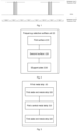
- Fig. 1 is a schematic diagram of the principle of an FSS-based A+P antenna scheme.
- a passive antenna surface working in an L frequency band an FSS and an active antenna surface working in an H frequency band are respectively provided.
- the FSS has the characteristics of low-impedance and high-pass for spatial electromagnetic waves, and can be used as a reflector for the passive antenna surface and a radome for the active antenna surface.
- the spatial filtering function of the FSS can reduce inter-frequency coupling between an L-band antenna and an H-band antenna, thereby improving the antenna performance.
- the FSS-based A+P antenna can ensure the independence of a 4G passive antenna surface and a 5G active antenna surface, i.e. support independent design, independent deployment, and independent maintenance of the active and passive antenna surfaces.
- Fig. 2 is a structural block diagram of a frequency selective surface unit according to embodiments of the present disclosure.
- the frequency selective surface unit 20 comprises: a first surface 210, composed of a plurality of first metal strips interleaved with one another; a second surface 220, composed of a plurality of second metal strips, wherein each of the second metal strips is provided with a second inter-strip gap, and metal strips at two sides of the second inter-strip gap are connected by means of a metal strip line, so as to form a parallel resonant LC circuit in an H frequency band; and a support plate 230, wherein the first surface 210 and the second surface 220 may be fixed on the same surface or front and back surfaces of the support plate 230.
- the first surface is composed of a plurality of first metal strips interleaved with one another;
- the second surface is composed of a plurality of second metal strips, wherein each of the second metal strips is provided with a second inter-strip gap, and metal strips at two sides of the second inter-strip gap are connected by means of a metal strip line, so as to form a parallel resonant LC circuit in an H frequency band; and the first surface and the second surface are fixed on the same surface or front and back surfaces of the support plate, thereby solving the problem in the related art that a 4G passive antenna surface cannot be perfectly integrated with a 5G active antenna surface.
- first inter-strip gaps are distributed at two ends of each first metal strip, and in cases where the first surface and the second surface are fixed on the front and back surfaces of the support plate, the second inter-strip gaps are located in a preset area above or below the first inter-strip gaps, so as to form a series resonant LC circuit in an L frequency band.
- the first inter-trip gaps may be symmetrically distributed at two ends of the first metal strip, and the second inter-trip gaps may be located right below the first inter-trip gaps.
- the positional relationship between the second inter-trip gaps and the first inter-trip gaps is not specifically limited, that is, the positional relationship between the first surface and the second surface is not limited.
- the second surface may be located right below the first surface, and may also be located right above the first surface; and the second surface may also be in the same layer as the first surface and distributed on the left side, the right side or the left and right sides of the first surface.
- Fig. 3 is a structural block diagram of a first metal strip of a first surface according to embodiments of the present disclosure.
- the first metal strip 30 further comprises: a first central metal strip 310 and two first side end metal strips 320, wherein the first central metal strip 310 is located in the middle of the first metal strip 30, and the two first side end metal strips 320 are respectively distributed at two ends of the first metal strip 30 and each forms a first inter-strip gap with the first central metal strip 310.
- the first metal strips 30 and/or the second metal strips 40 are at least one of the following: elongated metal strip lines; bent metal strip lines; metal coils; and metal via holes.
- the elongated metal strip line refers to a metal strip line of which the length is greater than or equal to five times the width.
- connection mode of the first metal strips 30 and the second metal strips 40 is one of the following: coplanar coupled line connection; non-coplanar coupled line connection; and interleaved line connection.
- the support plate is one of the following: a dielectric substrate; a ceramic; a sheet metal strip line; and a metal body.
- a frequency selective surface is provided, which is formed by periodic extension of the described frequency selective surface unit.
- the frequency selective surface is one of the following: single-layer periodic extension of the frequency selective surface unit; double-layer periodic extension of the frequency selective surface unit; and multi-layer periodic extension of the frequency selective surface unit.
- a spatial filtering method is provided, which is implemented using the described frequency selective surface.
- Fig. 5 is a flowchart of a spatial filtering method according to embodiments of the present disclosure. As shown in Fig. 5 , the flow comprises the following step: step S502: L values or C values of a series resonant LC circuit and a parallel resonant LC circuit are adjusted, so as to control a transmission frequency band and a reflection frequency band of a frequency selective surface unit.
- Fig. 6 is a flowchart of a spatial filtering method according to embodiments of the present disclosure. As shown in Fig. 6 , the flow comprises the following steps:
- the upper surface is the first surface
- the lower surface is the second surface
- the present scenario embodiment provides a low-impedance and high-pass FSS.
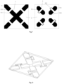
- Fig. 7 is a schematic structural diagram of an upper surface and a lower surface of an FSS unit according to scenario embodiments of the present disclosure.
- the FSS unit comprises an upper surface 1, a dielectric substrate 2 and a lower surface 3, and the dielectric substrate 2 supports the upper surface 1 and the lower surface 3.
- the upper surface 1 is composed of two first metal strips 11 interleaved with one another; and from the center to the outer side, each first metal strip 11 sequentially comprises a first central metal strip 111 and first side end metal strips 112.
- the lower surface 3 is formed by rotation of four second metal strips 31, and each second metal strip 31 comprises second side end metal strips 311, 313 and a second central metal strip 312.
- the second metal strips 31 are located right below the gaps between the first central metal strips 111 and the first side end metal strips 112. That is, as shown in Fig. 7 , the gaps between the second side end metal strips 311, 313 are exactly aligned with the gaps between the first central metal strips 111 and the first side end metal strips 112.
- Fig. 8 is a side view of a perspective structure of an FSS unit according to scenario embodiments of the present disclosure.
- the second metal strips 31 are located right below the gaps between the first central metal strips 111 and the first side end metal strips 112, which is used to implement the positional relationship that the lower surface is located right below the upper surface; however, the upper surface and the lower surface are not limited to this positional relationship.
- Each second central metal strip 312 has a width far less than the length, and may be equivalent to an inductor, for example, in the present embodiment, the range of "far less than” may be that the length of the metal strip is greater than or equal to five times the width; and the second side end metal strips 311, 313 are coupled to each other, and may be equivalent to a capacitor.
- the second central metal strip 312 and the second side end metal strips 311, 313 are connected in parallel, and may form a parallel resonant LC circuit in an H frequency band.
- Fig. 9 is a schematic structural diagram of an upper surface of an FSS according to scenario embodiments of the present disclosure
- Fig. 10 is a schematic structural diagram of a lower surface of the FSS according to scenario embodiments of the present disclosure.
- the FSS is formed by periodic extension of the FSS unit shown in Fig. 7 .
- the parallel resonant LC circuit In the H frequency band, the parallel resonant LC circuit is open to generate a reflection zero, so as to realize transmission of electromagnetic waves; and in the L frequency band, the series LC circuit is short-circuited to generate a transmission zero, so as to realize reflection of electromagnetic waves.
- Fig. 11 is a construction principle diagram of a four-order series-parallel resonant circuit according to scenario embodiments of the present disclosure. As shown in Fig. 11 , one-order, two-order or multi-order series-parallel resonant circuits can be constructed by increasing the number of metal strips 11.
- Fig. 12 is a schematic diagram of the shape of an FSS unit according to scenario embodiments of the present disclosure. As shown in Fig. 12 , the FSS unit is a rectangular FSS unit. A person skilled in the art should know that the shape of the FSS unit provided in some embodiments of the present disclosure may be a square, a rectangle, a triangle, or a polygon, which is not limited herein.
- Fig. 13 is a schematic structural diagram of a multi-layer FSS according to scenario embodiments of the present disclosure. As shown in Fig. 13 , the FSS may have a single-layer structure, a two-layer structure and a multi-layer structure.
- the FSS provided in some embodiments of the present disclosure realizes spatial filtering with low-impedance and high-pass characteristics by designing series LC circuits in an L frequency band and parallel LC circuits in an H frequency band.
- the series/parallel LC circuits and the equivalent capacitor and inductor elements are not limited to the forms described in scenario embodiment I, for example, the inductors may be designed as elongated straight lines, bent lines, coils, metal via holes, etc.; and the capacitors may be designed as coplanar coupled lines, non-coplanar coupled lines, interleaved lines, etc.
- the structures of series-parallel LC circuits are provided, but they are only described as examples, and are not specifically limited thereto.
- Fig. 14 is a schematic structural diagram of a distributed LC circuit according to scenario embodiments of the present disclosure.
- the distributed LC circuit comprises upper-layer and lower-layer metal strip lines, wherein a coupling region of the upper-layer metal strip line and the lower-layer metal strip line is equivalent to a capacitor, and the upper metal strip line is equivalent to an inductor.
- the structure can be regarded as a series LC circuit, and can provide a transmission zero in the L frequency band.
- Fig. 15 is a schematic structural diagram of a distributed LC circuit according to scenario embodiments of the present disclosure.
- the distributed LC circuit comprises a single-layer metal strip line, wherein the bent thin line in the middle is equivalent to an inductor, and wide lines on two sides are equivalent to a capacitor (it should be noted that the capacitor may be very small, and the corresponding line width is very narrow).
- the structure can be regarded as a parallel LC circuit, and can provide a reflection zero in the H frequency band.
- Fig. 16 is a schematic structural diagram of a distributed LC circuit according to scenario embodiments of the present disclosure.
- the distributed LC circuit comprises upper-layer and lower-layer metal strip lines, wherein the bent thin line in the middle of the lower-layer metal strip line is equivalent to an inductor, and metal strip lines on two sides of a thin seam are equivalent to a capacitor, and the two form a parallel LC circuit; and a coupling region of the upper-layer metal strip line and the lower-layer metal strip line is equivalent to a capacitor, and the upper metal strip line is equivalent to an inductor.
- the structure can be regarded as a parallel LC circuit and a series LC circuit, and can provide a transmission zero in the L frequency band and a reflection zero in the H frequency band.
- Fig. 17 is a schematic structural diagram of a distributed LC circuit according to scenario embodiments of the present disclosure.
- the distributed LC circuit comprises upper-layer and lower-layer metal strip lines, wherein the bent thin line at one side of the lower-layer metal strip line is equivalent to an inductor, and metal strip lines on two sides of a wide seam are equivalent to a capacitor, and the two form a parallel LC circuit; and a coupling region of the upper-layer metal strip line and the lower-layer metal strip line is equivalent to a capacitor, and the upper-layer metal strip line is equivalent to an inductor.
- the structure can be regarded as a parallel LC circuit and a series LC circuit, and can provide a transmission zero in the L frequency band and a reflection zero in the H frequency band.
- Fig. 18 is a schematic structural diagram of a distributed LC circuit according to scenario embodiments of the present disclosure.
- the distributed LC circuit comprises a single-layer metal strip line, wherein 1/4 wavelength open stub lines on two sides respectively form an equivalent inductor, and two stub lines are coupled with a metal strip line in the middle to form equivalent capacitors.
- the structure can be regarded as a parallel LC circuit, and can provide a reflection zero in the H frequency band.
- the present scenario embodiment provides a spatial filtering method.
- the resonant frequency of a parallel LC resonant circuit and a series LC resonant circuit can be changed by adjusting L values or C values, so as to control a transmission frequency band and a reflection frequency band; and N series resonant circuits and M parallel resonant circuits are constructed (N and M being greater than or equal to 1), and a transmission bandwidth and a reflection bandwidth can be respectively increased by increasing the value of N or M.
- Fig. 19 is a schematic structural diagram of an FSS unit according to scenario embodiments of the present disclosure. As shown in Fig. 19 , each of the two orthogonal metal strips of the FSS unit has four parallel LC circuits and two series LC circuits, and can provide four reflection zeros in the H frequency band and two transmission zeros in the L frequency band.
- Fig. 20 is a schematic structural diagram of an FSS unit according to scenario embodiments of the present disclosure.
- each of the two orthogonal metal strips of the FSS unit has four parallel LC circuits and two series LC circuits, and can provide four reflection zeros in the H frequency band and two transmission zeros in the L frequency band.
- the parallel LC circuit is formed by a bent inductive line and thin wires at two ends. As the thin lines at two ends have a narrow width, the capacitance thereof is small.
- the parallel LC circuit is approximately a pure inductor, it still relates to a parallel LC circuit in a strict sense.
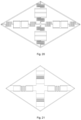
- Fig. 21 is a schematic structural diagram of an FSS unit according to scenario embodiments of the present disclosure
- Fig. 22 is a schematic structural diagram of an FSS unit according to scenario embodiments of the present disclosure.
- the FSS unit provided in the scenario embodiments above, a person skilled in the art should know that the FSS provided in some embodiments of the present disclosure has a plurality of structure implementation forms.
- a transmission zero and a reflection zero are respectively created in the L frequency band and the H frequency band, thereby achieving the functions of electromagnetic wave reflection in the L frequency band and electromagnetic wave transmission in the H frequency band.
- the FSS provided in some embodiments of the present disclosure has the following features: 1). the FSS can be applied to different carrier materials such as a dielectric substrate, a ceramic, a sheet metal strip line and a metal body; 2) the FSS may have a planar structure or a three-dimensional structure; 3) the FSS may have a single-layer structure or a multi-layer structure; 4) the shape of a unit may be a square, a rectangle, a triangle or a polygon; 5) a plurality of series or parallel resonant circuits may be constructed to obtain one or more transmission zeros or reflection zeros, thereby expanding the stopband and passband bandwidths; 6) only a parallel resonant circuit may be constructed to obtain an optimal reflection zero; and 7) dual-polarized, single-polarized and circularly-polarized electromagnetic waves may be supported.
- carrier materials such as a dielectric substrate, a ceramic, a sheet metal strip line and a metal body
- the FSS may have a planar structure or a three-dimensional
- the FSS designed according to some embodiments of the present disclosure can realize reflection with a relative bandwidth greater than 35% in the L frequency band, the reflection coefficient being greater than -0.2 dB, and can realize transmission with a relative bandwidth greater than 45% in the H frequency band, the transmission coefficient being greater than -0.3 dB.
- the frequency ratio of the L frequency band to the H frequency band can reach a minimum of 1.5:1 and a maximum of 5:1.
- the gain of a passive antenna surface in the L frequency band is only reduced by 0.2 dB, and the average gain of the active antennas in the H frequency band is not reduced.
- the FSS provided in the embodiments of the present disclosure is applicable to various specifications and models of active and passive integrated base stations and antenna products, and may be specifically used in the following scenarios: 1. a new site cannot be added; 2. a 5G antenna surface site cannot be added due to factors such as limited wind load; and 3. due to the effect of an early 4G antenna surface, the height of a 5G active antenna surface is relatively low or there are sites with line-of-sight obstructions.
- a transmission zero and a reflection zero are respectively obtained by constructing a low-frequency series LC circuit and a high-frequency parallel LC circuit in a metal strip, so as to achieve a low-impedance and high-pass filtering effect for spatial electromagnetic waves; and at the same time, on the basis of the FSS design method, a plurality of FSS unit embodiments are provided.
- the optimal embodiment uses a double-layer structure, which has extremely low transmission/reflection losses and good spatial dispersion characteristics, and can effectively suppress secondary radiation of an induced current in a wave-transmitting frequency band, thereby ensuring antenna surface air interface radiation characteristics.
- the frequency selective surface has the functions of reflecting low-frequency electromagnetic waves and transmitting high-frequency electromagnetic waves, can suppress inter-frequency coupling while implementing aperture sharing of multi-frequency antennas, and ensure independent deployment and separate maintenance of the multi-frequency antennas.
Landscapes
- Aerials With Secondary Devices (AREA)
Abstract
Description
- The present disclosure is based on Chinese patent application no.
CN 202211021650.5 filed on August 24, 2022 - Embodiments of the present disclosure relate to the field of communications, and in particular, to a frequency selective surface and a spatial filtering method.
- The deployment of a 5G active antenna surface faces three major challenges: 1. a new site cannot be added; 2. a 5G active antenna surface cannot be additionally deployed at an existing site deployed with a 4G passive antenna surface; and 3. a 5G active antenna surface can be additionally deployed at an existing site, but the limited height constraints optimal signal coverage. To this end, a 4G passive antenna surface and 5G active antenna surface integration scheme, i.e. an A+P (Active plus Passive, A+P) antenna, is proposed. The A+P antenna is a multi-frequency shared-aperture antenna that uses an integrated interleaving scheme to embed the 5G active antenna surface into the back of the 4G passive antenna surface, so as to achieve integrated deployment. The A+P antenna may be aligned with existing networks in performance, and supports separate maintenance and independent deployment of an active antenna surface and a passive antenna surface, thereby greatly reducing operation costs and satisfying the requirements of smooth device upgrade.
- In order to meet the A+P antenna performance, a frequency selective surface (FSS) needs to be designed to implement perfect integration of a passive antenna surface and an active antenna surface.
- Embodiments of the present disclosure provide a frequency selective surface and a spatial filtering method, so as to at least solve the problem in the related art that a 4G passive antenna surface cannot be perfectly integrated with a 5G active antenna surface.
- According to some embodiments of the present disclosure, a frequency selective surface unit is provided, comprising: a first surface, composed of a plurality of first metal strips interleaved with one another; a second surface, composed of a plurality of second metal strips, wherein each of the second metal strips is provided with a second inter-strip gap, and metal strips at two sides of the second inter-strip gap are connected by means of a metal strip line, so as to form a parallel resonant LC circuit in an H frequency band; and a support plate, the first surface and the second surface being fixed on the same surface or front and back surfaces of the support plate.
- According to some other embodiments of the present disclosure, a frequency selective surface is further provided, which is formed by periodic extension of the described frequency selective surface unit.
- According to still some other embodiments of the present disclosure, a spatial filtering method is further provided. The spatial filtering method is implemented using the described frequency selective surface, and comprises: L values or C values of a series resonant LC circuit and a parallel resonant LC circuit are adjusted, so as to control a transmission frequency band and a reflection frequency band of the frequency selective surface unit.
-
-
Fig. 1 is a schematic diagram of the principle of an FSS-based A+P antenna scheme according to embodiments of the present disclosure; -
Fig. 2 is a structural block diagram of a frequency selective surface unit according to embodiments of the present disclosure; -
Fig. 3 is a structural block diagram of a first metal strip of a first surface according to embodiments of the present disclosure; -
Fig. 4 is a structural block diagram of a second metal strip of a second surface according to embodiments of the present disclosure; -
Fig. 5 is a flowchart of a spatial filtering method according to embodiments of the present disclosure; -
Fig. 6 is a flowchart of a spatial filtering method according to embodiments of the present disclosure; -
Fig. 7 is a schematic structural diagram of an upper surface and a lower surface of an FSS unit according to scenario embodiments of the present disclosure; -
Fig. 8 is a side view of a perspective structure of an FSS unit according to scenario embodiments of the present disclosure; -
Fig. 9 is a schematic structural diagram of an upper surface of an FSS according to scenario embodiments of the present disclosure; -
Fig. 10 is a schematic structural diagram of a lower surface of an FSS according to scenario embodiments of the present disclosure; -
Fig. 11 is a construction principle diagram of a four-order series-parallel resonant circuit according to scenario embodiments of the present disclosure; -
Fig. 12 is a schematic diagram of the shape of an FSS unit according to embodiments of the present disclosure; -
Fig. 13 is a schematic structural diagram of a multi-layer FSS according to scenario embodiments of the present disclosure; -
Fig. 14 is a schematic structural diagram of a distributed LC circuit according to scenario embodiments of the present disclosure; -
Fig. 15 is a schematic structural diagram of a distributed LC circuit according to scenario embodiments of the present disclosure; -
Fig. 16 is a schematic structural diagram of a distributed LC circuit according to scenario embodiments of the present disclosure; -
Fig. 17 is a schematic structural diagram of a distributed LC circuit according to scenario embodiments of the present disclosure; -
Fig. 18 is a schematic structural diagram of a distributed LC circuit according to scenario embodiments of the present disclosure; -
Fig. 19 is a schematic structural diagram of an FSS unit according to scenario embodiments of the present disclosure; -
Fig. 20 is a schematic structural diagram of an FSS unit according to scenario embodiments of the present disclosure; -
Fig. 21 is a schematic structural diagram of an FSS unit according to scenario embodiments of the present disclosure; and -
Fig. 22 is a schematic structural diagram of an FSS unit according to scenario embodiments of the present disclosure. - Hereinafter, embodiments of the present disclosure are described in detail with reference to the accompanying drawings and in conjunction with the embodiments.
- It should be noted that the terms "first", "second", etc. in the description, claims, and accompanying drawings of the present disclosure are used to distinguish similar objects, and are not necessarily used to describe a specific sequence or order.
- An A+P antenna is a multi-frequency shared-aperture antenna that uses an integrated interleaving scheme to embed a 5G active antenna surface into the back of a 4G passive antenna surface, so as to achieve integrated deployment. The A+P antenna may be aligned with existing networks in performance, and supports separate maintenance and independent deployment of an active antenna surface and a passive antenna surface, thereby greatly reducing operation costs and satisfying the requirements of smooth device upgrade.
- A frequency selective surface (FSS) is a periodic artificial electromagnetic material, and can regulate and control electromagnetic waves with specific frequencies or polarized electromagnetic waves. By using the filtering function of an FSS for spatial electromagnetic waves, reflection of low-frequency signals (690-960 MHz, L frequency band) and transmission of high-frequency signals (2490-2690 MHz or 3400-3800 MHz, H frequency band) can be realized. The FSS technology can meet the development requirements of A+P products, and achieve perfect integration of passive and active antenna surfaces.
-
Fig. 1 is a schematic diagram of the principle of an FSS-based A+P antenna scheme. As shown inFig. 1 , from top to bottom, a passive antenna surface working in an L frequency band, an FSS and an active antenna surface working in an H frequency band are respectively provided. The FSS has the characteristics of low-impedance and high-pass for spatial electromagnetic waves, and can be used as a reflector for the passive antenna surface and a radome for the active antenna surface. At the same time, the spatial filtering function of the FSS can reduce inter-frequency coupling between an L-band antenna and an H-band antenna, thereby improving the antenna performance. Finally, the FSS-based A+P antenna can ensure the independence of a 4G passive antenna surface and a 5G active antenna surface, i.e. support independent design, independent deployment, and independent maintenance of the active and passive antenna surfaces. - The present embodiment provides a frequency selective surface unit.
Fig. 2 is a structural block diagram of a frequency selective surface unit according to embodiments of the present disclosure. As shown inFig. 2 , the frequencyselective surface unit 20 comprises: afirst surface 210, composed of a plurality of first metal strips interleaved with one another; asecond surface 220, composed of a plurality of second metal strips, wherein each of the second metal strips is provided with a second inter-strip gap, and metal strips at two sides of the second inter-strip gap are connected by means of a metal strip line, so as to form a parallel resonant LC circuit in an H frequency band; and asupport plate 230, wherein thefirst surface 210 and thesecond surface 220 may be fixed on the same surface or front and back surfaces of thesupport plate 230. - In the frequency selective surface unit provided in the foregoing embodiment of the present disclosure, the first surface is composed of a plurality of first metal strips interleaved with one another; the second surface is composed of a plurality of second metal strips, wherein each of the second metal strips is provided with a second inter-strip gap, and metal strips at two sides of the second inter-strip gap are connected by means of a metal strip line, so as to form a parallel resonant LC circuit in an H frequency band; and the first surface and the second surface are fixed on the same surface or front and back surfaces of the support plate, thereby solving the problem in the related art that a 4G passive antenna surface cannot be perfectly integrated with a 5G active antenna surface.
- In some exemplary embodiments, first inter-strip gaps are distributed at two ends of each first metal strip, and in cases where the first surface and the second surface are fixed on the front and back surfaces of the support plate, the second inter-strip gaps are located in a preset area above or below the first inter-strip gaps, so as to form a series resonant LC circuit in an L frequency band.
- In some embodiments of the present disclosure, the first inter-trip gaps may be symmetrically distributed at two ends of the first metal strip, and the second inter-trip gaps may be located right below the first inter-trip gaps. The positional relationship between the second inter-trip gaps and the first inter-trip gaps is not specifically limited, that is, the positional relationship between the first surface and the second surface is not limited. The second surface may be located right below the first surface, and may also be located right above the first surface; and the second surface may also be in the same layer as the first surface and distributed on the left side, the right side or the left and right sides of the first surface. The foregoing solution of the second surface being in the same layer as the first surface is only a change in the positional relationship, and the specific connection relationship and spatial coupling relationship involved may be the same as those when the second surface is located right below the first surface, that is, the series-parallel connection modes of elements for forming a parallel resonant LC circuit and a series resonant LC circuit are the same, which will not be further described herein.
- In some exemplary embodiments,
Fig. 3 is a structural block diagram of a first metal strip of a first surface according to embodiments of the present disclosure. As shown inFig. 3 , thefirst metal strip 30 further comprises: a firstcentral metal strip 310 and two first side end metal strips 320, wherein the firstcentral metal strip 310 is located in the middle of thefirst metal strip 30, and the two first side end metal strips 320 are respectively distributed at two ends of thefirst metal strip 30 and each forms a first inter-strip gap with the firstcentral metal strip 310. - In some exemplary embodiments,
Fig. 4 is a structural block diagram of a second metal strip of a second surface according to embodiments of the present disclosure. As shown inFig. 4 , thesecond metal strip 40 further comprises: two second side end metal strips 410, wherein the two second side end metal strips 410 are distributed at two sides of the second inter-strip gap and are connected by means of themetal strip line 420. - In some exemplary embodiments, the second inter-strip gaps being located in a preset area above or below the first inter-strip gaps so as to form a series resonant LC circuit in an L frequency band comprises: a first
central metal strip 310, two first side end metal strips 320, two second side end metal strips 410 and ametal strip line 420 are connected in series, so as to form the series resonant LC circuit in the L frequency band. - In some exemplary embodiments, the first metal strips 30 and/or the second metal strips 40 are at least one of the following: elongated metal strip lines; bent metal strip lines; metal coils; and metal via holes. In some embodiments of the present disclosure, the elongated metal strip line refers to a metal strip line of which the length is greater than or equal to five times the width.
- In some exemplary embodiments, the connection mode of the first metal strips 30 and the second metal strips 40 is one of the following: coplanar coupled line connection; non-coplanar coupled line connection; and interleaved line connection.
- In some exemplary embodiments, the support plate is one of the following: a dielectric substrate; a ceramic; a sheet metal strip line; and a metal body.
- According to some other embodiments of the present disclosure, a frequency selective surface is provided, which is formed by periodic extension of the described frequency selective surface unit.
- In some exemplary embodiments, the frequency selective surface is one of the following: single-layer periodic extension of the frequency selective surface unit; double-layer periodic extension of the frequency selective surface unit; and multi-layer periodic extension of the frequency selective surface unit.
- According to still some other embodiments of the present disclosure, a spatial filtering method is provided, which is implemented using the described frequency selective surface.
Fig. 5 is a flowchart of a spatial filtering method according to embodiments of the present disclosure. As shown inFig. 5 , the flow comprises the following step:
step S502: L values or C values of a series resonant LC circuit and a parallel resonant LC circuit are adjusted, so as to control a transmission frequency band and a reflection frequency band of a frequency selective surface unit. - In some exemplary embodiments,
Fig. 6 is a flowchart of a spatial filtering method according to embodiments of the present disclosure. As shown inFig. 6 , the flow comprises the following steps: - step S602: L values or C values of a series resonant LC circuit and a parallel resonant LC circuit are adjusted, so as to control a transmission frequency band and a reflection frequency band of a frequency selective surface unit; and
- step S604: the number of series resonant LC circuits and parallel resonant LC circuits are adjusted, so as to control a transmission bandwidth and a reflection bandwidth of the frequency selective surface unit.
- A person skilled in the art should know that the execution order of the described steps may be interchanged, which is not specifically limited herein.
- To make a person skilled in the art better understand the technical solutions of the present disclosure, hereinafter, the technical solutions will be described in conjunction with specific scenario embodiments. In some scenario embodiments of the present disclosure, the upper surface is the first surface, and the lower surface is the second surface.
- The present scenario embodiment provides a low-impedance and high-pass FSS.
-
Fig. 7 is a schematic structural diagram of an upper surface and a lower surface of an FSS unit according to scenario embodiments of the present disclosure. As shown inFig. 7 , in the present scenario embodiment, the FSS unit comprises anupper surface 1, a dielectric substrate 2 and alower surface 3, and the dielectric substrate 2 supports theupper surface 1 and thelower surface 3. Theupper surface 1 is composed of two first metal strips 11 interleaved with one another; and from the center to the outer side, eachfirst metal strip 11 sequentially comprises a firstcentral metal strip 111 and first side end metal strips 112. Thelower surface 3 is formed by rotation of four second metal strips 31, and each second metal strip 31 comprises second side end metal strips 311, 313 and a secondcentral metal strip 312. The second metal strips 31 are located right below the gaps between the firstcentral metal strips 111 and the first side end metal strips 112. That is, as shown inFig. 7 , the gaps between the second side end metal strips 311, 313 are exactly aligned with the gaps between the firstcentral metal strips 111 and the first side end metal strips 112. -
Fig. 8 is a side view of a perspective structure of an FSS unit according to scenario embodiments of the present disclosure. A person skilled in the art should know that in the present scenario embodiment, the second metal strips 31 are located right below the gaps between the firstcentral metal strips 111 and the first side end metal strips 112, which is used to implement the positional relationship that the lower surface is located right below the upper surface; however, the upper surface and the lower surface are not limited to this positional relationship. - Each second
central metal strip 312 has a width far less than the length, and may be equivalent to an inductor, for example, in the present embodiment, the range of "far less than" may be that the length of the metal strip is greater than or equal to five times the width; and the second side end metal strips 311, 313 are coupled to each other, and may be equivalent to a capacitor. The secondcentral metal strip 312 and the second side end metal strips 311, 313 are connected in parallel, and may form a parallel resonant LC circuit in an H frequency band. - The second side end metal strips 311, 313 are respectively coupled to the first
central metal strip 111 and the first sideend metal strip 112, and may be equivalent to capacitors; and the firstcentral metal strip 111, the first sideend metal strip 112, and the secondcentral metal strip 312 may be equivalent to inductors. The firstcentral metal strip 111, the first side end metal strips 112, the second side end metal strips 311, 313 and the secondcentral metal strip 312 are connected in series, and may form a series resonant LC circuit in an L frequency band. -
Fig. 9 is a schematic structural diagram of an upper surface of an FSS according to scenario embodiments of the present disclosure; andFig. 10 is a schematic structural diagram of a lower surface of the FSS according to scenario embodiments of the present disclosure. As shown inFigs. 9 and10 , the FSS is formed by periodic extension of the FSS unit shown inFig. 7 . - In the H frequency band, the parallel resonant LC circuit is open to generate a reflection zero, so as to realize transmission of electromagnetic waves; and in the L frequency band, the series LC circuit is short-circuited to generate a transmission zero, so as to realize reflection of electromagnetic waves.
-
Fig. 11 is a construction principle diagram of a four-order series-parallel resonant circuit according to scenario embodiments of the present disclosure. As shown inFig. 11 , one-order, two-order or multi-order series-parallel resonant circuits can be constructed by increasing the number of metal strips 11. -
Fig. 12 is a schematic diagram of the shape of an FSS unit according to scenario embodiments of the present disclosure. As shown inFig. 12 , the FSS unit is a rectangular FSS unit. A person skilled in the art should know that the shape of the FSS unit provided in some embodiments of the present disclosure may be a square, a rectangle, a triangle, or a polygon, which is not limited herein. -
Fig. 13 is a schematic structural diagram of a multi-layer FSS according to scenario embodiments of the present disclosure. As shown inFig. 13 , the FSS may have a single-layer structure, a two-layer structure and a multi-layer structure. - The FSS provided in some embodiments of the present disclosure realizes spatial filtering with low-impedance and high-pass characteristics by designing series LC circuits in an L frequency band and parallel LC circuits in an H frequency band. The series/parallel LC circuits and the equivalent capacitor and inductor elements are not limited to the forms described in scenario embodiment I, for example, the inductors may be designed as elongated straight lines, bent lines, coils, metal via holes, etc.; and the capacitors may be designed as coplanar coupled lines, non-coplanar coupled lines, interleaved lines, etc. Hereinafter, several examples of the structures of series-parallel LC circuits are provided, but they are only described as examples, and are not specifically limited thereto.
-
Fig. 14 is a schematic structural diagram of a distributed LC circuit according to scenario embodiments of the present disclosure. As shown inFig. 14 , the distributed LC circuit comprises upper-layer and lower-layer metal strip lines, wherein a coupling region of the upper-layer metal strip line and the lower-layer metal strip line is equivalent to a capacitor, and the upper metal strip line is equivalent to an inductor. The structure can be regarded as a series LC circuit, and can provide a transmission zero in the L frequency band. -
Fig. 15 is a schematic structural diagram of a distributed LC circuit according to scenario embodiments of the present disclosure. As shown inFig. 15 , the distributed LC circuit comprises a single-layer metal strip line, wherein the bent thin line in the middle is equivalent to an inductor, and wide lines on two sides are equivalent to a capacitor (it should be noted that the capacitor may be very small, and the corresponding line width is very narrow). The structure can be regarded as a parallel LC circuit, and can provide a reflection zero in the H frequency band. -
Fig. 16 is a schematic structural diagram of a distributed LC circuit according to scenario embodiments of the present disclosure. As shown inFig. 16 , the distributed LC circuit comprises upper-layer and lower-layer metal strip lines, wherein the bent thin line in the middle of the lower-layer metal strip line is equivalent to an inductor, and metal strip lines on two sides of a thin seam are equivalent to a capacitor, and the two form a parallel LC circuit; and a coupling region of the upper-layer metal strip line and the lower-layer metal strip line is equivalent to a capacitor, and the upper metal strip line is equivalent to an inductor. The structure can be regarded as a parallel LC circuit and a series LC circuit, and can provide a transmission zero in the L frequency band and a reflection zero in the H frequency band. -
Fig. 17 is a schematic structural diagram of a distributed LC circuit according to scenario embodiments of the present disclosure. As shown inFig. 17 , the distributed LC circuit comprises upper-layer and lower-layer metal strip lines, wherein the bent thin line at one side of the lower-layer metal strip line is equivalent to an inductor, and metal strip lines on two sides of a wide seam are equivalent to a capacitor, and the two form a parallel LC circuit; and a coupling region of the upper-layer metal strip line and the lower-layer metal strip line is equivalent to a capacitor, and the upper-layer metal strip line is equivalent to an inductor. The structure can be regarded as a parallel LC circuit and a series LC circuit, and can provide a transmission zero in the L frequency band and a reflection zero in the H frequency band. -
Fig. 18 is a schematic structural diagram of a distributed LC circuit according to scenario embodiments of the present disclosure. As shown inFig. 18 , the distributed LC circuit comprises a single-layer metal strip line, wherein 1/4 wavelength open stub lines on two sides respectively form an equivalent inductor, and two stub lines are coupled with a metal strip line in the middle to form equivalent capacitors. The structure can be regarded as a parallel LC circuit, and can provide a reflection zero in the H frequency band. - A person skilled in the art should know that the distributed LC circuit structures provided above can be used to replace the overlapping part of the projections of the metal wires or metal strips on the upper and lower surfaces of the FSS unit in the direction perpendicular to the dielectric substrate.
- The present scenario embodiment provides a spatial filtering method. The resonant frequency of a parallel LC resonant circuit and a series LC resonant circuit can be changed by adjusting L values or C values, so as to control a transmission frequency band and a reflection frequency band; and N series resonant circuits and M parallel resonant circuits are constructed (N and M being greater than or equal to 1), and a transmission bandwidth and a reflection bandwidth can be respectively increased by increasing the value of N or M.
-
Fig. 19 is a schematic structural diagram of an FSS unit according to scenario embodiments of the present disclosure. As shown inFig. 19 , each of the two orthogonal metal strips of the FSS unit has four parallel LC circuits and two series LC circuits, and can provide four reflection zeros in the H frequency band and two transmission zeros in the L frequency band. -
Fig. 20 is a schematic structural diagram of an FSS unit according to scenario embodiments of the present disclosure. As shown inFig. 20 , each of the two orthogonal metal strips of the FSS unit has four parallel LC circuits and two series LC circuits, and can provide four reflection zeros in the H frequency band and two transmission zeros in the L frequency band. The parallel LC circuit is formed by a bent inductive line and thin wires at two ends. As the thin lines at two ends have a narrow width, the capacitance thereof is small. Although the parallel LC circuit is approximately a pure inductor, it still relates to a parallel LC circuit in a strict sense. -
Fig. 21 is a schematic structural diagram of an FSS unit according to scenario embodiments of the present disclosure; andFig. 22 is a schematic structural diagram of an FSS unit according to scenario embodiments of the present disclosure. - According to the schematic structural diagram of the FSS unit provided in the scenario embodiments above, a person skilled in the art should know that the FSS provided in some embodiments of the present disclosure has a plurality of structure implementation forms.
- In some embodiments of the present disclosure, by constructing on a periodic metal strip a distributed LC circuit that has a series resonance characteristic in the L frequency band and a parallel resonance characteristic in the H frequency band, a transmission zero and a reflection zero are respectively created in the L frequency band and the H frequency band, thereby achieving the functions of electromagnetic wave reflection in the L frequency band and electromagnetic wave transmission in the H frequency band. By using the method, not only can the characteristics of low-impedance and high-pass for spatial electromagnetic waves be obtained, but also electromagnetic scattering in the H frequency band can be suppressed, thereby ensuring that an antenna working in the H frequency band achieves an excellent conformal radiation pattern effect.
- In conclusion, the FSS provided in some embodiments of the present disclosure has the following features: 1). the FSS can be applied to different carrier materials such as a dielectric substrate, a ceramic, a sheet metal strip line and a metal body; 2) the FSS may have a planar structure or a three-dimensional structure; 3) the FSS may have a single-layer structure or a multi-layer structure; 4) the shape of a unit may be a square, a rectangle, a triangle or a polygon; 5) a plurality of series or parallel resonant circuits may be constructed to obtain one or more transmission zeros or reflection zeros, thereby expanding the stopband and passband bandwidths; 6) only a parallel resonant circuit may be constructed to obtain an optimal reflection zero; and 7) dual-polarized, single-polarized and circularly-polarized electromagnetic waves may be supported.
- The FSS designed according to some embodiments of the present disclosure can realize reflection with a relative bandwidth greater than 35% in the L frequency band, the reflection coefficient being greater than -0.2 dB, and can realize transmission with a relative bandwidth greater than 45% in the H frequency band, the transmission coefficient being greater than -0.3 dB. The frequency ratio of the L frequency band to the H frequency band can reach a minimum of 1.5:1 and a maximum of 5:1. In joint simulation with passive antennas in the L frequency band and active antennas in the H frequency band, the gain of a passive antenna surface in the L frequency band is only reduced by 0.2 dB, and the average gain of the active antennas in the H frequency band is not reduced.
- The FSS provided in the embodiments of the present disclosure is applicable to various specifications and models of active and passive integrated base stations and antenna products, and may be specifically used in the following scenarios: 1. a new site cannot be added; 2. a 5G antenna surface site cannot be added due to factors such as limited wind load; and 3. due to the effect of an early 4G antenna surface, the height of a 5G active antenna surface is relatively low or there are sites with line-of-sight obstructions.
- According to the FSS provided in some embodiments of the present disclosure, a transmission zero and a reflection zero are respectively obtained by constructing a low-frequency series LC circuit and a high-frequency parallel LC circuit in a metal strip, so as to achieve a low-impedance and high-pass filtering effect for spatial electromagnetic waves; and at the same time, on the basis of the FSS design method, a plurality of FSS unit embodiments are provided. The optimal embodiment uses a double-layer structure, which has extremely low transmission/reflection losses and good spatial dispersion characteristics, and can effectively suppress secondary radiation of an induced current in a wave-transmitting frequency band, thereby ensuring antenna surface air interface radiation characteristics. The frequency selective surface has the functions of reflecting low-frequency electromagnetic waves and transmitting high-frequency electromagnetic waves, can suppress inter-frequency coupling while implementing aperture sharing of multi-frequency antennas, and ensure independent deployment and separate maintenance of the multi-frequency antennas.
- The content above merely relates to preferred embodiments of the present disclosure and is not intended to limit embodiments of the present disclosure. For a person skilled in the art, embodiments of the present disclosure may have various modifications and variations. Any modifications, equivalent replacements, improvements, etc. made within the principle of embodiments of the present disclosure shall all fall within the scope of protection of embodiments of the present disclosure.
Claims (12)
- A frequency selective surface unit, comprising:a first surface, composed of a plurality of first metal strips interleaved with one another;a second surface, composed of a plurality of second metal strips, wherein each of the second metal strips is provided with a second inter-strip gap, and metal strips at two sides of the second inter-strip gap are connected by means of a metal strip line, so as to form a parallel resonant LC circuit in an H frequency band; anda support plate, the first surface and the second surface being fixed on the same surface or front and back surfaces of the support plate.
- The frequency selective surface unit according to claim 1, wherein first inter-strip gaps are distributed at two ends of each of the first metal strips, and in cases where the first surface and the second surface are fixed on the front and back surfaces of the support plate, the second inter-strip gaps are located in a preset area above or below the first inter-strip gaps, so as to form a series resonant LC circuit in an L frequency band.
- The frequency selective surface unit according to claim 1, wherein the first metal strips each comprise: a first central metal strip and two first side end metal strips; and the first central metal strip is located in the middle of the first metal strip, and the two first side end metal strips are respectively distributed at two ends of the first metal strip and each forms a first inter-strip gap with the first central metal strip.
- The frequency selective surface unit according to claim 1, wherein the second metal strips each comprise:
two second side end metal strips, and the two second side end metal strips are distributed at two sides of the second inter-strip gap and are connected by means of the metal strip line. - The frequency selective surface unit according to claim 2, wherein the second inter-strip gaps being located in a preset area above or below the first inter-strip gaps so as to form a series resonant LC circuit in an L frequency band comprises:
a first central metal strip, two first side end metal strips, two second side end metal strips and the metal strip line are connected in series, so as to form the series resonant LC circuit in the L frequency band. - The frequency selective surface unit according to claim 1, wherein the first metal strips and/or the second metal strips are at least one of the following:elongated metal strip lines;bent metal strip lines;metal coils; andmetal via holes.
- The frequency selective surface unit according to claim 1, wherein the connection mode of the first metal strips and the second metal strips is one of the following:coplanar coupled line connection;non-coplanar coupled line connection; andinterleaved line connection.
- The frequency selective surface unit according to claim 1, wherein the support plate is one of the following:a dielectric substrate;a ceramic;a sheet metal strip line; anda metal body.
- A frequency selective surface, formed by periodic extension of the frequency selective surface unit according to any one of claims 1-8.
- The frequency selective surface according to claim 9, wherein the frequency selective surface comprises one of the following:single-layer periodic extension of the frequency selective surface unit;double-layer periodic extension of the frequency selective surface unit; andmulti-layer periodic extension of the frequency selective surface unit.
- A spatial filtering method, implemented using the frequency selective surface according to claim 10, comprising:
adjusting L values or C values of a series resonant LC circuit and a parallel resonant LC circuit, so as to control a transmission frequency band and a reflection frequency band of the frequency selective surface unit. - The method according to claim 11, further comprising:
adjusting the number of series resonant LC circuits and parallel resonant LC circuits, so as to control a transmission bandwidth and a reflection bandwidth of the frequency selective surface unit.
Applications Claiming Priority (2)
| Application Number | Priority Date | Filing Date | Title |
|---|---|---|---|
| CN202211021650.5A CN117673762A (en) | 2022-08-24 | 2022-08-24 | Frequency Selective Surfaces and Spatial Filtering Methods |
| PCT/CN2023/108731 WO2024041280A1 (en) | 2022-08-24 | 2023-07-21 | Frequency selective surface and spatial filtering method |
Publications (2)
| Publication Number | Publication Date |
|---|---|
| EP4564609A1 true EP4564609A1 (en) | 2025-06-04 |
| EP4564609A4 EP4564609A4 (en) | 2025-11-19 |
Family
ID=90012386
Family Applications (1)
| Application Number | Title | Priority Date | Filing Date |
|---|---|---|---|
| EP23856370.4A Pending EP4564609A4 (en) | 2022-08-24 | 2023-07-21 | FREQUENCY-SELECTIVE SURFACE AND SPATIAL FILTERING METHOD |
Country Status (3)
| Country | Link |
|---|---|
| EP (1) | EP4564609A4 (en) |
| CN (1) | CN117673762A (en) |
| WO (1) | WO2024041280A1 (en) |
Families Citing this family (2)
| Publication number | Priority date | Publication date | Assignee | Title |
|---|---|---|---|---|
| CN118137168B (en) * | 2024-03-25 | 2024-08-16 | 南京林业大学 | Two-dimensional and three-dimensional mixed structure frequency selective absorber with broadband transmission and broadband wave absorption |
| CN119764849A (en) * | 2024-03-27 | 2025-04-04 | 中兴通讯股份有限公司 | Frequency selection unit, frequency selection surface and base station antenna |
Family Cites Families (6)
| Publication number | Priority date | Publication date | Assignee | Title |
|---|---|---|---|---|
| US20030142036A1 (en) * | 2001-02-08 | 2003-07-31 | Wilhelm Michael John | Multiband or broadband frequency selective surface |
| US7071889B2 (en) * | 2001-08-06 | 2006-07-04 | Actiontec Electronics, Inc. | Low frequency enhanced frequency selective surface technology and applications |
| CN103490175B (en) * | 2013-09-23 | 2016-01-06 | 摩比天线技术(深圳)有限公司 | A kind of integrated base station antenna |
| CN110416735A (en) * | 2018-07-16 | 2019-11-05 | 西安电子科技大学 | Flexible multi-layered frequency-selective surfaces with transmission zero |
| CN111786122A (en) * | 2020-07-26 | 2020-10-16 | 中国人民解放军国防科技大学 | A reconfigurable wave-absorbing and wave-transmitting integrated FSS with high transmittance |
| CN215680980U (en) * | 2021-09-29 | 2022-01-28 | 京信通信技术(广州)有限公司 | Passive antenna and multi-frequency fusion base station antenna |
-
2022
- 2022-08-24 CN CN202211021650.5A patent/CN117673762A/en active Pending
-
2023
- 2023-07-21 WO PCT/CN2023/108731 patent/WO2024041280A1/en not_active Ceased
- 2023-07-21 EP EP23856370.4A patent/EP4564609A4/en active Pending
Also Published As
| Publication number | Publication date |
|---|---|
| EP4564609A4 (en) | 2025-11-19 |
| CN117673762A (en) | 2024-03-08 |
| WO2024041280A1 (en) | 2024-02-29 |
Similar Documents
| Publication | Publication Date | Title |
|---|---|---|
| JP7734838B2 (en) | Controllable electromagnetic array elements and intelligence surfaces | |
| CN111864368B (en) | Low-profile broadband circularly polarized antenna for 5G communication and design method thereof | |
| CN113285226B (en) | A low frequency radiation unit and antenna | |
| EP4564609A1 (en) | Frequency selective surface and spatial filtering method | |
| US12176632B2 (en) | Dual-polarized filtering antenna units and dual-polarized filtering antenna arrays | |
| CN115864003B (en) | A frequency selective surface with wide-band reconfigurable wave-transmitting window | |
| CN106299628B (en) | Antenna and wireless router | |
| CN118040336B (en) | Broadband wave-transparent filtering low-frequency radiation unit, common-caliber antenna array and communication equipment | |
| CN113346250A (en) | Millimeter wave three-frequency selection surface based on multilayer coupling structure | |
| CN112563724A (en) | Low-profile half-mode substrate integrated waveguide filter antenna with high frequency selectivity | |
| CN113036432A (en) | Pilot frequency filtering antenna, manufacturing method and application of pilot frequency filtering antenna | |
| CN116742356A (en) | 5G millimeter wave dual-band antenna based on multi-layer metasurface | |
| CN116722355B (en) | A dual-polarized filter antenna, an array antenna, and a wireless communication device | |
| CN115693172A (en) | An intelligent reflective surface unit with broadband and low loss and intelligent reflective surface | |
| CN113497357B (en) | A broadband dual-polarized filter antenna | |
| CN112134005A (en) | Dipole antenna and wireless device | |
| CN215497086U (en) | A kind of low frequency radiation unit and antenna | |
| CN111952722A (en) | A reflection array antenna unit, reflection array antenna and manufacturing method | |
| CN117458157A (en) | An intelligent metasurface with filtering function and its design method | |
| CN117394008A (en) | Ultra-wideband antenna with notch structure and design method thereof | |
| CN118763413B (en) | A dual-polarized filter antenna | |
| CN116565545A (en) | Antenna and Network Equipment | |
| CN120498409B (en) | Spatial non-resonant node resonator, filter and radio frequency communication equipment | |
| CN223871692U (en) | Radiating elements, antennas, and base stations | |
| CN103594766B (en) | Miniaturization coplanar compact type electromagnetic band gap structure |
Legal Events
| Date | Code | Title | Description |
|---|---|---|---|
| STAA | Information on the status of an ep patent application or granted ep patent |
Free format text: STATUS: THE INTERNATIONAL PUBLICATION HAS BEEN MADE |
|
| PUAI | Public reference made under article 153(3) epc to a published international application that has entered the european phase |
Free format text: ORIGINAL CODE: 0009012 |
|
| STAA | Information on the status of an ep patent application or granted ep patent |
Free format text: STATUS: REQUEST FOR EXAMINATION WAS MADE |
|
| 17P | Request for examination filed |
Effective date: 20250226 |
|
| AK | Designated contracting states |
Kind code of ref document: A1 Designated state(s): AL AT BE BG CH CY CZ DE DK EE ES FI FR GB GR HR HU IE IS IT LI LT LU LV MC ME MK MT NL NO PL PT RO RS SE SI SK SM TR |
|
| A4 | Supplementary search report drawn up and despatched |
Effective date: 20251022 |
|
| RIC1 | Information provided on ipc code assigned before grant |
Ipc: H01Q 15/00 20060101AFI20251016BHEP Ipc: H01Q 1/24 20060101ALN20251016BHEP |
|
| DAV | Request for validation of the european patent (deleted) | ||
| DAX | Request for extension of the european patent (deleted) |