EP4560480A2 - Système et procédé de défragmentation de dispositif de mémoire - Google Patents
Système et procédé de défragmentation de dispositif de mémoire Download PDFInfo
- Publication number
- EP4560480A2 EP4560480A2 EP25169706.6A EP25169706A EP4560480A2 EP 4560480 A2 EP4560480 A2 EP 4560480A2 EP 25169706 A EP25169706 A EP 25169706A EP 4560480 A2 EP4560480 A2 EP 4560480A2
- Authority
- EP
- European Patent Office
- Prior art keywords
- addresses
- file
- memory
- host
- lba
- Prior art date
- Legal status (The legal status is an assumption and is not a legal conclusion. Google has not performed a legal analysis and makes no representation as to the accuracy of the status listed.)
- Pending
Links
Images



Classifications
-
- G—PHYSICS
- G06—COMPUTING OR CALCULATING; COUNTING
- G06F—ELECTRIC DIGITAL DATA PROCESSING
- G06F3/00—Input arrangements for transferring data to be processed into a form capable of being handled by the computer; Output arrangements for transferring data from processing unit to output unit, e.g. interface arrangements
- G06F3/06—Digital input from, or digital output to, record carriers, e.g. RAID, emulated record carriers or networked record carriers
- G06F3/0601—Interfaces specially adapted for storage systems
- G06F3/0628—Interfaces specially adapted for storage systems making use of a particular technique
- G06F3/0655—Vertical data movement, i.e. input-output transfer; data movement between one or more hosts and one or more storage devices
- G06F3/0658—Controller construction arrangements
-
- G—PHYSICS
- G06—COMPUTING OR CALCULATING; COUNTING
- G06F—ELECTRIC DIGITAL DATA PROCESSING
- G06F12/00—Accessing, addressing or allocating within memory systems or architectures
- G06F12/02—Addressing or allocation; Relocation
- G06F12/0223—User address space allocation, e.g. contiguous or non contiguous base addressing
- G06F12/023—Free address space management
- G06F12/0238—Memory management in non-volatile memory, e.g. resistive RAM or ferroelectric memory
- G06F12/0246—Memory management in non-volatile memory, e.g. resistive RAM or ferroelectric memory in block erasable memory, e.g. flash memory
-
- G—PHYSICS
- G06—COMPUTING OR CALCULATING; COUNTING
- G06F—ELECTRIC DIGITAL DATA PROCESSING
- G06F12/00—Accessing, addressing or allocating within memory systems or architectures
- G06F12/02—Addressing or allocation; Relocation
- G06F12/0223—User address space allocation, e.g. contiguous or non contiguous base addressing
- G06F12/0292—User address space allocation, e.g. contiguous or non contiguous base addressing using tables or multilevel address translation means
-
- G—PHYSICS
- G06—COMPUTING OR CALCULATING; COUNTING
- G06F—ELECTRIC DIGITAL DATA PROCESSING
- G06F3/00—Input arrangements for transferring data to be processed into a form capable of being handled by the computer; Output arrangements for transferring data from processing unit to output unit, e.g. interface arrangements
- G06F3/06—Digital input from, or digital output to, record carriers, e.g. RAID, emulated record carriers or networked record carriers
- G06F3/0601—Interfaces specially adapted for storage systems
- G06F3/0602—Interfaces specially adapted for storage systems specifically adapted to achieve a particular effect
- G06F3/0604—Improving or facilitating administration, e.g. storage management
-
- G—PHYSICS
- G06—COMPUTING OR CALCULATING; COUNTING
- G06F—ELECTRIC DIGITAL DATA PROCESSING
- G06F3/00—Input arrangements for transferring data to be processed into a form capable of being handled by the computer; Output arrangements for transferring data from processing unit to output unit, e.g. interface arrangements
- G06F3/06—Digital input from, or digital output to, record carriers, e.g. RAID, emulated record carriers or networked record carriers
- G06F3/0601—Interfaces specially adapted for storage systems
- G06F3/0602—Interfaces specially adapted for storage systems specifically adapted to achieve a particular effect
- G06F3/0608—Saving storage space on storage systems
-
- G—PHYSICS
- G06—COMPUTING OR CALCULATING; COUNTING
- G06F—ELECTRIC DIGITAL DATA PROCESSING
- G06F3/00—Input arrangements for transferring data to be processed into a form capable of being handled by the computer; Output arrangements for transferring data from processing unit to output unit, e.g. interface arrangements
- G06F3/06—Digital input from, or digital output to, record carriers, e.g. RAID, emulated record carriers or networked record carriers
- G06F3/0601—Interfaces specially adapted for storage systems
- G06F3/0602—Interfaces specially adapted for storage systems specifically adapted to achieve a particular effect
- G06F3/061—Improving I/O performance
- G06F3/0611—Improving I/O performance in relation to response time
-
- G—PHYSICS
- G06—COMPUTING OR CALCULATING; COUNTING
- G06F—ELECTRIC DIGITAL DATA PROCESSING
- G06F3/00—Input arrangements for transferring data to be processed into a form capable of being handled by the computer; Output arrangements for transferring data from processing unit to output unit, e.g. interface arrangements
- G06F3/06—Digital input from, or digital output to, record carriers, e.g. RAID, emulated record carriers or networked record carriers
- G06F3/0601—Interfaces specially adapted for storage systems
- G06F3/0628—Interfaces specially adapted for storage systems making use of a particular technique
- G06F3/0638—Organizing or formatting or addressing of data
- G06F3/064—Management of blocks
-
- G—PHYSICS
- G06—COMPUTING OR CALCULATING; COUNTING
- G06F—ELECTRIC DIGITAL DATA PROCESSING
- G06F3/00—Input arrangements for transferring data to be processed into a form capable of being handled by the computer; Output arrangements for transferring data from processing unit to output unit, e.g. interface arrangements
- G06F3/06—Digital input from, or digital output to, record carriers, e.g. RAID, emulated record carriers or networked record carriers
- G06F3/0601—Interfaces specially adapted for storage systems
- G06F3/0628—Interfaces specially adapted for storage systems making use of a particular technique
- G06F3/0655—Vertical data movement, i.e. input-output transfer; data movement between one or more hosts and one or more storage devices
- G06F3/0659—Command handling arrangements, e.g. command buffers, queues, command scheduling
-
- G—PHYSICS
- G06—COMPUTING OR CALCULATING; COUNTING
- G06F—ELECTRIC DIGITAL DATA PROCESSING
- G06F3/00—Input arrangements for transferring data to be processed into a form capable of being handled by the computer; Output arrangements for transferring data from processing unit to output unit, e.g. interface arrangements
- G06F3/06—Digital input from, or digital output to, record carriers, e.g. RAID, emulated record carriers or networked record carriers
- G06F3/0601—Interfaces specially adapted for storage systems
- G06F3/0668—Interfaces specially adapted for storage systems adopting a particular infrastructure
- G06F3/0671—In-line storage system
- G06F3/0673—Single storage device
- G06F3/0679—Non-volatile semiconductor memory device, e.g. flash memory, one time programmable memory [OTP]
-
- G—PHYSICS
- G06—COMPUTING OR CALCULATING; COUNTING
- G06F—ELECTRIC DIGITAL DATA PROCESSING
- G06F2206/00—Indexing scheme related to dedicated interfaces for computers
- G06F2206/10—Indexing scheme related to storage interfaces for computers, indexing schema related to group G06F3/06
- G06F2206/1004—Defragmentation
-
- G—PHYSICS
- G06—COMPUTING OR CALCULATING; COUNTING
- G06F—ELECTRIC DIGITAL DATA PROCESSING
- G06F2212/00—Indexing scheme relating to accessing, addressing or allocation within memory systems or architectures
- G06F2212/10—Providing a specific technical effect
- G06F2212/1016—Performance improvement
-
- G—PHYSICS
- G06—COMPUTING OR CALCULATING; COUNTING
- G06F—ELECTRIC DIGITAL DATA PROCESSING
- G06F2212/00—Indexing scheme relating to accessing, addressing or allocation within memory systems or architectures
- G06F2212/10—Providing a specific technical effect
- G06F2212/1016—Performance improvement
- G06F2212/1024—Latency reduction
-
- G—PHYSICS
- G06—COMPUTING OR CALCULATING; COUNTING
- G06F—ELECTRIC DIGITAL DATA PROCESSING
- G06F2212/00—Indexing scheme relating to accessing, addressing or allocation within memory systems or architectures
- G06F2212/10—Providing a specific technical effect
- G06F2212/1032—Reliability improvement, data loss prevention, degraded operation etc
-
- G—PHYSICS
- G06—COMPUTING OR CALCULATING; COUNTING
- G06F—ELECTRIC DIGITAL DATA PROCESSING
- G06F2212/00—Indexing scheme relating to accessing, addressing or allocation within memory systems or architectures
- G06F2212/10—Providing a specific technical effect
- G06F2212/1041—Resource optimization
- G06F2212/1044—Space efficiency improvement
-
- G—PHYSICS
- G06—COMPUTING OR CALCULATING; COUNTING
- G06F—ELECTRIC DIGITAL DATA PROCESSING
- G06F2212/00—Indexing scheme relating to accessing, addressing or allocation within memory systems or architectures
- G06F2212/21—Employing a record carrier using a specific recording technology
- G06F2212/214—Solid state disk
-
- G—PHYSICS
- G06—COMPUTING OR CALCULATING; COUNTING
- G06F—ELECTRIC DIGITAL DATA PROCESSING
- G06F2212/00—Indexing scheme relating to accessing, addressing or allocation within memory systems or architectures
- G06F2212/72—Details relating to flash memory management
- G06F2212/7201—Logical to physical mapping or translation of blocks or pages
-
- G—PHYSICS
- G06—COMPUTING OR CALCULATING; COUNTING
- G06F—ELECTRIC DIGITAL DATA PROCESSING
- G06F2212/00—Indexing scheme relating to accessing, addressing or allocation within memory systems or architectures
- G06F2212/72—Details relating to flash memory management
- G06F2212/7205—Cleaning, compaction, garbage collection, erase control
-
- Y—GENERAL TAGGING OF NEW TECHNOLOGICAL DEVELOPMENTS; GENERAL TAGGING OF CROSS-SECTIONAL TECHNOLOGIES SPANNING OVER SEVERAL SECTIONS OF THE IPC; TECHNICAL SUBJECTS COVERED BY FORMER USPC CROSS-REFERENCE ART COLLECTIONS [XRACs] AND DIGESTS
- Y02—TECHNOLOGIES OR APPLICATIONS FOR MITIGATION OR ADAPTATION AGAINST CLIMATE CHANGE
- Y02D—CLIMATE CHANGE MITIGATION TECHNOLOGIES IN INFORMATION AND COMMUNICATION TECHNOLOGIES [ICT], I.E. INFORMATION AND COMMUNICATION TECHNOLOGIES AIMING AT THE REDUCTION OF THEIR OWN ENERGY USE
- Y02D10/00—Energy efficient computing, e.g. low power processors, power management or thermal management
Definitions
- the present disclosure relates to systems and methods for defragmentation of a memory device.
- Defragmentation is a process that reduces the degree of fragmentation by reorganizing a storage device's data for faster access and better system performance.
- the memory controller includes a controller memory for storing a logical-to-physical (L2P) address mapping table corresponding to a file, and a controller processor configured to control a memory device, receive a mapping update command, and update the L2P address mapping table according to the mapping update command by replacing original logical addresses of logical block address (LBA) segments of the file with new continuous logical addresses of a merged LBA segment of the file, and changing an original mapping relation between the original logical addresses of the LBA segment of the file and physical addresses of the file, to a new mapping relation between the new continuous logical addresses of the merged LBA segment of the file and the physical addresses of the file.
- LBA logical block address
- the controller memory includes a volatile controller memory for storing the L2P address mapping table corresponding to the file.
- the controller memory further includes a non-volatile controller memory.
- the controller processor is configured to store the updated L2P address mapping table in the non-volatile controller memory as a non-volatile L2P address mapping table.
- the controller processor is configured to transmit an instruction to a host acknowledging that the L2P address mapping table has been updated.
- the controller processor is configured to generate a merge log by recording the new mapping relation between the new continuous logical addresses of the merged LBA segment of the file and the physical addresses of the file.
- the controller processor in response to a sudden power loss, is configured to rebuild the volatile L2P address mapping table according to a merge log recording the new mapping relation between the new continuous logical addresses of the merged LBA segment of the file the physical addresses of the file after a memory system being restarted.
- the controller processor is configured to scan a physical-to-logical (P2L) address mapping table of a metadata block and the merge log, and in response to the merge log being updated, the controller processor is configured to rebuild the L2P address mapping table according to the merge log.
- P2L physical-to-logical
- a memory system in another aspect, includes a memory device including a physical data block, and a memory controller including a controller memory for storing a logical-to-physical (L2P) address mapping table corresponding to a file, and a controller processor configured to control the memory device, receive a mapping update command, and update the L2P address mapping table according to the mapping update command by replacing original logical addresses of logical block address (LBA) segments of the file with new continuous logical addresses of a merged LBA segment of the file, and changing an original mapping relation between the original logical addresses of the LBA segment of the file and physical addresses of the file, to a new mapping relation between the new continuous logical addresses of the merged LBA segment of the file and the physical addresses of the file.
- LBA logical block address
- the controller memory includes a volatile controller memory for storing the L2P address mapping table corresponding to the file.
- the controller memory further includes a non-volatile controller memory.
- the controller processor is configured to store the updated the L2P address mapping table in the non-volatile controller memory as a non-volatile L2P address mapping table.
- the controller processor is configured to transmit an instruction to a host acknowledging that the L2P address mapping table has been updated.
- the controller processor is configured to generate a merge log by recording the new mapping relation between the new continuous logical addresses of the merged LBA segment of the file and the physical addresses of the file.
- the controller processor in response to a sudden power loss, is configured to rebuild the L2P address mapping table according to a merge log recording the new mapping relation between the new continuous logical addresses of the merged LBA segment of the file the physical addresses of the file after the memory system being restarted.
- the controller processor is configured to scan a physical-to-logical (P2L) address mapping table of a metadata block and the merge log, and in response to the merge log being updated, the controller processor is configured to rebuild the L2P address mapping table according to the merge log.
- P2L physical-to-logical
- a system in still another aspect, includes a host including a host memory configured to store a file, and a host processor configured to execute a merge LBA command to rearrange original logical addresses of logical block address (LBA) segments of the file into new continuous logical addresses of a merged LBA segment of the file and send a mapping update command, and a memory system including a memory device comprising a physical data block, and a memory controller including a controller memory for storing a logical-to-physical (L2P) address mapping table corresponding to the file, and a controller processor configured to control the memory device, receive the mapping update command, and update the L2P address mapping table according to the mapping update command by replacing the original logical addresses of the LBA segments of the file with the new continuous logical addresses of the merged LBA segment of the file, and changing an original mapping relation between the original logical addresses of the LBA segment of the file and physical addresses of the file, to a new mapping relation between the new continuous logical addresses of the merged LBA segment of the file and the
- the controller memory includes a volatile controller memory for storing the L2P address mapping table corresponding to the file.
- the host processor is configured to rearrange the original logical addresses of the LBA segments of the file into the new logical addresses of the merged LBA segment of the file by rewriting all logical addresses of the LBA segments of the file into a free or unused LBA segment with logical addresses in continuous and sequential order such that it becomes new continuous logical addresses of the merged LBA segment of the file.
- the host processor is configured to send the mapping update command causing the memory controller to update the L2P address mapping table according to new continuous logical addresses of the merged LBA segment of the file.
- the host processor is configured to receive an instruction from the memory controller acknowledging that the L2P address mapping table has been updated.
- the host processor is configured to update an index node of the file after acknowledging that the L2P address mapping table has been updated.
- the host processor is configured to update the index node of the file by pointing to a new LBA segment with the new continuous logical addresses of the merged LBA segment.
- a method for operating a memory controller includes receiving a mapping update command from a host, and updating a logical-to-physical (L2P) address mapping table according to the mapping update command by replacing the original logical addresses of the LBA segments of the file with the new continuous logical addresses of the merged LBA segment of the file, and changing an original mapping relation between the original logical addresses of the LBA segment of the file and physical addresses of the file, to a new mapping relation between the new continuous logical addresses of the merged LBA segment of the file and the physical addresses of the file.
- L2P logical-to-physical
- the method further includes transmitting an instruction to the host acknowledging that the L2P address mapping table has been updated.
- the method further includes recording, in a merge log, the new mapping relation between the new continuous logical addresses of the merged LBA segment of the file and the physical addresses of the file, and in response to a sudden power loss, rebuilding the L2P address mapping table according to the merge log after a memory system is restarted.
- rebuilding the L2P address mapping table includes scanning a physical-to-logical (P2L) address mapping table of a metadata block and the merge log, and in response to determining that the merge log being updated, rebuilding the L2P address mapping table according to the merge log.
- P2L physical-to-logical
- terminology may be understood at least in part from usage in context.
- the term “one or more” as used herein, depending at least in part upon context may be used to describe any feature, structure, or characteristic in a singular sense or may be used to describe combinations of features, structures or characteristics in a plural sense.
- terms, such as “a,” “an,” or “the,” again, may be understood to convey a singular usage or to convey a plural usage, depending at least in part upon context.
- the term “based on” may be understood as not necessarily intended to convey an exclusive set of factors and may, instead, allow for existence of additional factors not necessarily expressly described, again, depending at least in part on context.
- Disk defragmentation is a technique that allows users to defragment not only hard disk drive (HDD) but also other removable storage.
- Windows system such as Windows 7
- Microsoft Drive Optimizer or Disk Defragmenter that allows users to defrag their hard disk and increase the data access speed by rearranging files stored on the disk to occupy contiguous storage locations and improve computer's overall performance.
- Disk defragmentation does not deem effective in solid-state drive (SSD). In fact, it is generally not recommended to defrag an SSD since it may use up write cycles of the SSD and potentially causes early death of the SSD.
- the input/output stack (I/O stack) of software (SW) becomes a bottleneck of the system. That is, the fragmented file at the logical level reduces the performance of the system.
- the e2defrag may read every segment of the logical address of a file and select a continuous logical address block to write.
- the e2defrag may not only update the logical address block but also update the physical block each time updating the logical address block, thereby increasing an effect of write amplification, which is an undesirable phenomenon associated with flash memory and solid-state drives where the actual amount of information physically written to the storage media is a multiple of the logical amount intended to be written.
- This write amplification may burn out the SSD fast than expected and shorten the lifespan of the SSD.
- conventional e2defrag is time-consuming due to its lengthy process of reading segments and routinely updating the physical address block each time updating the logical address block. It is not effective enough to solve the fragmentation problem at the logical level.
- conventional defragmentation tools may not have a very well design for power loss protection to ensure that the data is not lost while the SSD is writing data when a sudden power failure occurs.
- the sudden power loss may cause significant system corruption or data loss when the process of defragmentation is undergoing.
- a mechanism to prevent data loss from sudden power loss during defragmentation is highly desirable.
- the present disclosure introduces a solution in which a merged logical block address (LBA) command is designed to merge segments of LBA in a file into a merged LBA segment of the file and update a logical to physical (L2P) address mapping table according to the merged LBA segments of the file. Furthermore, a merge log is created to record a mapping relation between the L2P address mapping table and the physical-to-logical (P2L) address mapping table before updating the L2P address mapping table. Therefore, after a sudden power loss, the L2P can be rebuilt or restored by using the merge log and the P2L address mapping table.
- LBA merged logical block address
- P2L physical-to-logical
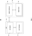
- FIG. 1 illustrates a block diagram of an exemplary system 100 having a memory device, according to some aspects of the present disclosure.
- System 100 can be a mobile phone, a desktop computer, a laptop computer, a tablet, a vehicle computer, a gaming console, a printer, a positioning device, a wearable electronic device, a smart sensor, a virtual reality (VR) device, an argument reality (AR) device, or any other suitable electronic devices having storage therein.
- system 100 can include a host 108 having a host memory 110 and a host processor 112, and a memory system 102 having one or more memory devices 104 and a memory controller 106.
- Host 108 can be a processor of an electronic device, such as a central processing unit (CPU), or a system-on-chip (SoC), such as an application processor (AP).
- Host 108 can be coupled to memory controller 106 and configured to send or receive data to or from memory devices 104 through memory controller 106.
- Host processor 112 can be a control unit (CU), or an arithmetic & logic unit (ALU).
- Host memory 110 can be memory units including register or cache memory.
- Host 108 is configured to receive and transmit instructions and commands to and from memory controller 106 of memory device 102, and execute or perform multiple functions and operations provided in the present disclosure, which will be described later.
- Memory device 104 can be any memory device disclosed in the present disclosure, such as a NAND Flash memory device, which includes a page buffer having multiple portions, for example, four quarters. It is noted that the NAND Flash is only one example of the memory device for illustrative purposes. It can include any suitable solid-state, non-volatile memory, e.g., NOR Flash, Ferroelectric RAM (FeRAM), Phase-change memory (PCM), Magnetoresistive random-access memory (MRAM), Spin-transfer torque magnetic random-access memory (STT-RAM), or Resistive random-access memory (RRAM), etc. In some implementations, memory device 104 includes a three-dimensional (3D) NAND Flash memory device.
- 3D three-dimensional
- Memory controller 106 can be implemented by microprocessors, microcontrollers (a.k.a. microcontroller units (MCUs)), digital signal processors (DSPs), application-specific integrated circuits (ASICs), field-programmable gate arrays (FPGAs), programmable logic devices (PLDs), state machines, gated logic, discrete hardware circuits, and other suitable hardware, firmware, and/or software configured to perform the various functions described below in detail.
- MCUs microcontrollers
- DSPs digital signal processors
- ASICs application-specific integrated circuits
- FPGAs field-programmable gate arrays
- PLDs programmable logic devices
- state machines gated logic, discrete hardware circuits, and other suitable hardware, firmware, and/or software configured to perform the various functions described below in detail.
- Memory controller 106 is coupled to memory device 104 and host 108 and is configured to control memory device 104, according to some implementations. Memory controller 106 can manage the data stored in memory device 104 and communicate with host 108. In some implementations, memory controller 106 is designed for operating in a low duty-cycle environment like secure digital (SD) cards, compact Flash (CF) cards, universal serial bus (USB) Flash drives, or other media for use in electronic devices, such as personal computers, digital cameras, mobile phones, etc. In some implementations, memory controller 106 is designed for operating in a high duty-cycle environment SSDs or embedded multi-media-cards (eMMCs) used as data storage for mobile devices, such as smartphones, tablets, laptop computers, etc., and enterprise storage arrays.
- SSDs secure digital
- CF compact Flash
- USB universal serial bus
- Memory controller 106 can be configured to control operations of memory device 104, such as read, erase, and program operations, by providing instructions, such as read instructions, to memory device 104.
- memory controller 106 may be configured to provide a read instruction to the peripheral circuit of memory device 104 to control the read operation.
- Memory controller 106 can also be configured to manage various functions with respect to the data stored or to be stored in memory device 104 including, but not limited to bad-block management, garbage collection, logical-to-physical address conversion, wear leveling, etc.
- memory controller 106 is further configured to process error correction codes (ECCs) with respect to the data read from or written to memory device 104. Any other suitable functions may be performed by memory controller 106 as well, for example, formatting memory device 104.
- ECCs error correction codes
- Memory controller 106 can communicate with an external device (e.g., host 108) according to a particular communication protocol.
- memory controller 106 may communicate with the external device through at least one of various interface protocols, such as a USB protocol, an MMC protocol, a peripheral component interconnection (PCI) protocol, a PCI-express (PCI-E) protocol, an advanced technology attachment (ATA) protocol, a serial-ATA protocol, a parallel-ATA protocol, a small computer small interface (SCSI) protocol, an enhanced small disk interface (ESDI) protocol, an integrated drive electronics (IDE) protocol, a Firewire protocol, etc.
- various interface protocols such as a USB protocol, an MMC protocol, a peripheral component interconnection (PCI) protocol, a PCI-express (PCI-E) protocol, an advanced technology attachment (ATA) protocol, a serial-ATA protocol, a parallel-ATA protocol, a small computer small interface (SCSI) protocol, an enhanced small disk interface (ESDI) protocol, an integrated drive electronics (IDE) protocol, a Fire
- Memory controller 106 and one or more memory devices 104 can be integrated into various types of storage devices, for example, being included in the same package, such as a universal Flash storage (UFS) package or an eMMC package. That is, memory system 102 can be implemented and packaged into different types of end electronic products.
- memory controller 106 and a single memory device 104 may be integrated into a memory card 202.
- Memory card 202 can include a PC card (PCMCIA, personal computer memory card international association), a CF card, a smart media (SM) card, a memory stick, a multimedia card (MMC, RS-MMC, MMCmicro), an SD card (SD, miniSD, microSD, SDHC), a UFS, etc.
- Memory card 202 can further include a memory card connector 204 coupling memory card 202 with a host (e.g., host 108 in FIG. 1 ).
- memory controller 106 and multiple memory devices 104 may be integrated into an SSD 206.
- SSD 206 can further include an SSD connector 208 coupling SSD 206 with a host (e.g., host 108 in FIG. 1 ).
- the storage capacity and/or the operation speed of SSD 206 is greater than those of memory card 202.
- Memory control 106 is configured to receive and transmit a command to and from host 108, and execute or perform multiple functions and operations provided in the present disclosure, which will be described later.
- FIG. 3 illustrates a schematic circuit diagram of an exemplary memory device 300 including peripheral circuits, according to some aspects of the present disclosure.
- Memory device 300 can be an example of memory device 104 in FIG. 1 . It is noted that the NAND Flash disclosed herein is only one example of the memory device for illustrative purposes. It can include any suitable solid-state, non-volatile memory, e.g., NOR Flash, FeRAM, PCM, MRAM, STT-RAM, or RRAM, etc.
- Memory device 300 can include a memory cell array 301 and peripheral circuits 302 coupled to memory cell array 301.
- Memory cell array 301 can be a NAND Flash memory cell array in which memory cells 306 are provided in the form of an array of NAND memory strings 308 each extending vertically above a substrate (not shown).
- each NAND memory string 308 includes a plurality of memory cells 306 coupled in series and stacked vertically.
- Each memory cell 306 can hold a continuous, analog value, such as an electrical voltage or charge, which depends on the number of electrons trapped within a region of memory cell 306.
- Each memory cell 306 can be either a floating gate type of memory cell including a floating-gate transistor or a charge trap type of memory cell including a charge-trap transistor.
- each memory cell 306 is a single-level cell (SLC) that has two possible memory states and thus, can store one bit of data.
- the first memory state "0" can correspond to a first range of voltages
- the second memory state "1" can correspond to a second range of voltages.
- each memory cell 306 is a multi-level cell (MLC) that is capable of storing more than a single bit of data in more than four memory states.
- the MLC can store two bits per cell, three bits per cell (also known as triple-level cell (TLC)), or four bits per cell (also known as a quad-level cell (QLC)).
- TLC triple-level cell
- QLC quad-level cell
- Each MLC can be programmed to assume a range of possible nominal storage values. In one example, if each MLC stores two bits of data, then the MLC can be programmed to assume one of three possible programming levels from an erased state by writing one of three possible nominal storage values to the cell. A fourth nominal storage value can be used for the
- each NAND memory string 308 can include a source select gate (SSG) transistor 310 at its source end and a drain select gate (DSG) transistor 312 at its drain end.
- SSG transistor 310 and DSG transistor 312 can be configured to activate selected NAND memory strings 308 (columns of the array) during read and program operations.
- the sources of NAND memory strings 308 in the same block 304 are coupled through a same source line (SL) 314, e.g., a common SL.
- SL source line
- all NAND memory strings 308 in the same block 304 have an array common source (ACS), according to some implementations.
- ACS array common source
- each NAND memory string 308 is configured to be selected or deselected by applying a select voltage (e.g., above the threshold voltage of DSG transistor 312) or a deselect voltage (e.g., 0 V) to the gate of respective DSG transistor 312 through one or more DSG lines 313 and/or by applying a select voltage (e.g., above the threshold voltage of SSG transistor 310) or a deselect voltage (e.g., 0 V) to the gate of respective SSG transistor 310 through one or more SSG lines 315.
- a select voltage e.g., above the threshold voltage of DSG transistor 312
- a deselect voltage e.g., 0 V
- NAND memory strings 308 can be organized into multiple blocks 304, each of which can have a common source line 314, e.g., coupled to the ACS.
- each block 304 is the basic data unit for erase operations, i.e., all memory cells 306 on the same block 304 are erased at the same time.
- source lines 314 coupled to selected block 304 as well as unselected blocks 304 in the same plane as selected block 304 can be biased with an erase voltage (Vers), such as a high positive voltage (e.g., 20 V or more).
- Memory cells 306 of adjacent NAND memory strings 308 can be coupled through word lines 318 that select which row of memory cells 306 is affected by the read and program operations.
- each word line 318 is coupled to a page 320 of memory cells 306, which is the basic data unit for the program and read operations.
- the size of one page 320 in bits can relate to the number of NAND memory strings 308 coupled by word line 318 in one block 304.
- Each word line 318 can include a plurality of control gates (gate electrodes) at each memory cell 306 in respective page 320 and a gate line coupling the control gates.
- Peripheral circuits 302 can be coupled to memory cell array 301 through bit lines 316, word lines 318, source lines 314, SSG lines 315, and DSG lines 313.
- Peripheral circuits 302 can include any suitable analog, digital, and mixed-signal circuits for facilitating the operations of memory cell array 301 by applying and sensing voltage signals and/or current signals to and from each target memory cell 306 through bit lines 316, word lines 318, source lines 314, SSG lines 315, and DSG lines 313.
- Peripheral circuits 302 can include various types of peripheral circuits formed using metal-oxide-semiconductor (MOS) technologies.
- MOS metal-oxide-semiconductor
- FIG. 4A illustrates a block diagram of an exemplary memory system 102 including a memory controller 106 and a memory device 104, according to some aspects of the present disclosure.
- memory controller 106 can include a controller processor 408, such as a memory chip controller (MCC) or a memory controller unit (MCU).
- Controller processor 408 is configured to control modules to execute commands or instructions to perform functions disclosed in the present disclosure.
- Controller processor 408 can also be configured to control the operations of each peripheral circuit by generating and sending various control signals, such as read commands for read operations.
- Controller processor 408 can also send clock signals at desired frequencies, periods, and duty cycles to other peripheral circuits 302 to orchestrate the operations of each peripheral circuit 302, for example, for synchronization.
- Memory controller 106 can further include a volatile controller memory 411 and a non-volatile controller memory.
- Volatile controller memory 411 can include a register or cache memory such that it allows a faster access and process speed to read, write, or erase the data stored therein, while it may not retain stored information after power is removed.
- volatile controller memory 411 includes dynamic random-access memory (DRAM), Static random-access memory (SRAM).
- Non-volatile controller memory 413 can retain the stored information even after power is removed.
- non-volatile controller memory 413 includes NAND, NOR, FeRAM, PCM, MRAM, STT-RAM, or RRAM.
- Memory device 104 can include a memory cell array such as memory cell array 301 in FIG. 3 .
- non-volatile controller memory 413 can be not provided in the memory controller 106, for example, non-volatile controller memory 413 is deposed outside of the memory controller 106 but is coupled to the memory controller 106.
- the controller memory e.g., 411 or 413 is configured to store the L2P address mapping table (e.g., 4271, 4273) corresponding to the file (e.g., 129).
- FIG. 4B illustrates a block diagram of the exemplary memory system 102 including memory controller 106 and memory device 104, according to some aspects of the present disclosure.
- memory controller 106 can include a memory controller interface 429 configured to receive and transmit commands or instructions to and from the host (e.g., host 108 in FIG. 1 ).
- memory controller interface 429 is coupled to the controller processor 408 and to receive and transmit commands or instructions that cause controller processor 408 to perform functions disclosed in the present disclosure.
- Memory controller 106 can also include an updating module 421 configured to generate and update a volatile L2P address mapping table 4271, a volatile merge log 4251, a non-volatile L2P mapping table 4273, and a non-volatile merge log 4253.
- Updating module 421 may be implemented through a firmware program in the firmware of controller processor 408.
- updating module 421 is configured to update a physical data block 431 and/or a metadata block 433 in memory device 104.
- updating module 421 is in controller processor 408 or coupled to controller processor 408, and may be controlled by controller processor 408 to execute commands and instructions from host 108.
- updating module 421 is configured to execute a mapping update command received from host 108 and update volatile L2P address mapping table 4271 according to the mapping update command.
- updating module 421 is configured to update volatile L2P address mapping table 4271 by rewriting a continuous logical address of a merged LBA segment of a file into volatile L2P address mapping table 4271.
- updating module 421 is configured to update volatile L2P address mapping table 4271 by replacing original logical addresses of LBA segments of the file 129 with new continuous logical addresses of a merged LBA segment of the file, and changing an original mapping relation between the original logical addresses of the LBA segment of the file and physical addresses of the file, to a new mapping relation between the new continuous logical addresses of the merged LBA segment of the file and the physical addresses of the file.
- the process of forming the continuous logical address of the merged LBA segments of the file will be described later.
- updating module 421 in controller processor 408 will transmit an instruction correspondingly to host 108 acknowledging that volatile L2P address mapping table 4271 has been updated, so that host 108 may update the index node of the file in host memory 110.
- volatile L2P address mapping table 4271 is stored and processed in volatile controller memory 411 and is configured to be transmitted and updated to non-volatile L2P address mapping table 4273 stored in physical data block 431 so that the data will not be erased after power off.
- volatile L2P address mapping table 4271 in volatile controller memory 411 can be loaded from non-volatile L2P address mapping table 4273 in physical data block 431 for faster access and processing speed on a regular basis.
- non-volatile L2P address mapping table 4273 can also be stored in non-volatile controller memory 413 of memory controller 106.
- Merge log (e.g., volatile merge log 4251 and non-volatile merge log 4253) is configured to record a mapping relation between the L2P address mapping table (e.g., 4271 or 4273) and the physical address of physical data block 431 before the updating of the L2P address mapping table.
- the merge log is configured to record a new mapping relation between the new continuous logical addresses of the merged LBA segment of file 129 and the physical addresses of file 129 each updating the L2P address mapping table.
- volatile L2P address mapping table 4271 which may not be updated yet, can be rebuilt or restored by using non-volatile merge log 4253 and the physical address of physical data block 431 after the system (e.g., 100) is restarted. It is noted that, in some implementations, the updating rate of non-volatile merge log 4253 is faster than non-volatile L2P address mapping table 4273 such that it is already recorded during a sudden power loss while it may not cause excessive write amplification since it is relatively small data comparing to non-volatile L2P address mapping table 4273.
- a recovery module 423 in controller processor 408 may scan a physical-to-logical (P2L) address mapping table 435 in metadata block 433 in memory device 104 and non-volatile merge log 4253, and in response to that non-volatile merge log 4253 being updated, rebuild volatile L2P address mapping table 4271 according to non-volatile merge log 4253 and the physical address of physical data block 431 retained before the sudden power loss. And in response to that non-volatile merge log 4253 is not updated, rebuild volatile L2P address mapping table 4271 according to physical-to-logical (P2L) address mapping table 435 of metadata block 433 and the physical address of physical data block 431 retained before the sudden power loss.
- P2L physical-to-logical
- Metadata block 433 is a relatively small piece of a data block in memory cell array 301.
- Metadata block 433 is configured to store logical address information of the data stored in physical data block 431. The logical address information is written into metadata block 433 simultaneously when writing data into physical data block 431 so that it can recover data after the sudden power loss.
- volatile merge log 4251 is stored and processed in volatile controller memory 411 and is configured to be transmitted and updated to non-volatile merge log 4253 stored in physical data block 431 so that the data will not be erased after power off.
- volatile merge 4251 in volatile controller memory 411 can be loaded from non-volatile merge log 4253 in physical data block 431 for faster access and processing speed on a regular basis.
- non-volatile merge log 4253 can also be stored in non-volatile controller memory 413 of memory controller 106.
- Recovery module 423 may be implemented through a firmware program in the firmware of controller processor 408.
- FIG. 5 illustrates a block diagram of the exemplary system 100 including host 108 and memory controller 106, according to some aspects of the present disclosure.
- host 108 may include a host interface 125, host memory 110, and host processor 112.
- Host interface 125 is configured to receive commands or instructions from a user to perform or execute specific functions or operations.
- Host memory 110 may store logical addresses, e.g., a logical block address (LBA) of files (e.g., file 129), and an index node 127 (e.g., inode) of the files.
- Host processor 112 may include or be coupled to an index node updating module 121 (e.g., inode updating module) and a merge LBA module 123.
- LBA logical block address
- Index node updating module 121 is configured to update index node 127 of the files after controller processor 408 (e.g., in FIG. 4B ) of memory controller 106 transmits an instruction to host 108, acknowledging that volatile L2P address mapping table 4271 has been updated. Index node updating module 121 can also update index node 127 of the files after receiving an instruction that physical data block 431 (e.g., in FIG. 4B ) has been updated. It is noted that the index node (e.g., inode) may be a data structure in a Unix-style file system that describes a file-system object such as a file or a directory. It can be a file data structure that stores information about any Linux file except its name and data.
- host processor 112 is configured to update index node 127 of file 129 by pointing to a new LBA segment with the continuous logical addresses of the merged LBA segment.
- Merge LBA module 123 that is included or coupled to host processor 112 is configured to execute a merge LBA command to rearrange the LBA segments (e.g., fragments of the logical address in a logical block) of file 129 into a merged LBA segment.
- file A 129 may include one or more LBA segments (e.g., LBA segment 1, LBA segment 2, LBA segment 3..., LBA segment N).
- Merge LBA module 123 may therefore execute a merge LBA command to rearrange the LBA segments of file 129 into a merged LBA segment.
- rearranging the LBA segment of file 129 includes rewriting all logical addresses of the LBA segments of file 129 into a free or unused logical address block (e.g., free or unused LBA segments) in continuous and sequential order such that it becomes a continuous logical address block (e.g., a merged LBA segment).
- the merged LBA segment will not be used to update the physical data block (e.g., physical data block 431 in FIG. 4B ).
- the merged LBA segment is used to only update volatile L2P address mapping table 4271 in FIG. 4B . By doing so, since there is no updating physical data block each time updating logical address block, the write amplification is minimized.
- host processor 112 may send a mapping update command causing controller processor (e.g., 408 in FIG. 4A ) in memory controller 106 to update volatile L2P address mapping table 4271 according to the merged LBA segment.
- controller processor e.g., 408 in FIG. 4A
- volatile L2P address mapping table 4271 with originally discontinuous and discrete logical addresses e.g., LBA 9, LBA 11, LBA 13, LBA 18
- LBA segments e.g., LBA 9, LBA 11, LBA 13, LBA 18
- LBA segments e.g., LBA 9, LBA 11, LBA 13, LBA 18
- the physical addresses (e.g., PA 333, PA 337, PA 339, PA 440) of the updated volatile L2P address mapping table 4271 directed to corresponding physical addresses of physical data block 431 remain unchanged in the above updating process. Therefore, after the defragmentation process, physical data block 431 has not been written and remains the same.
- FIG. 8 illustrates a block diagram illustrating an exemplary defragmentation scheme under sudden power loss, according to some aspects of the present disclosure.
- volatile L2P address mapping table 4271 may not be updated or fail to complete the current updating, and therefore the data may be lost since the physical data is not updated as well.
- a metadata block e.g., metadata block 433 in FIG. 4B
- a memory device e.g., memory device 104
- P2L mapping table e.g., P2L address mapping table 435 in FIG. 4B
- the physical addresses of outdated L2P address mapping table e.g., LBA 9, LBA 11, LBA 13, LBA 18).
- non-volatile merge log 4253 stores a mapping relation between P2L address mapping table 435 and volatile L2P address mapping table 4271 (e.g., LBA 9 of P2L points to LBA 114 of new L2P, LBA 11 of P2L points to LBA 115 of new L2P, LBA 13 of P2L points to LBA 116 if new L2P, LBA 18 of P2L points to LBA 117 of new L2P) after each updating volatile L2P address mapping table 4271, a new volatile L2P address mapping table 4271 can be rebuilt by using non-volatile merge log 4253 and the retained P2L address mapping table 435 according to the mapping relation.
- P2L address mapping table 435 e.g., LBA 9 of P2L points to LBA 114 of new L2P, LBA 11 of P2L points to LBA 115 of new L2P, LBA 13 of P2L points to LBA 116 if new L2P, LBA 18 of P2L points
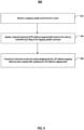
- FIG. 9 illustrates a flowchart of an exemplary method for operating a memory controller, according to some aspects of the present disclosure.
- the memory controller may be any suitable memory controller disclosed herein, e.g., memory controller 106 in FIG. 4B .
- Method 900 may be implemented partially or fully by memory controller 106 as in FIG. 4A . It is understood that the operations shown in method 900 may not be exhaustive and that other operations can be performed as well before, after, or between any of the illustrated operations. Further, some of the operations may be performed simultaneously, or in a different order than shown in FIG. 9 .
- method 900 starts at operation 902 in which a memory controller (e.g., memory controller 106 as in FIG. 4A ) receives a mapping update command from a host (e.g., host 108 in FIG. 5 ).
- the mapping update command may cause memory controller 106 to start updating module 421.
- Method 900 proceeds to operation 904, as illustrated in FIG. 9 , in which an L2P address mapping table (e.g., volatile L2P address mapping table 4271 in FIG. 4B ) stored in memory controller 106 is updated according to the mapping update command.
- updating the L2P address mapping table includes rewriting a continuous logical address of a merged LBA segment of a file (e.g., file 129 in FIGs. 5-7 ) into the L2P address mapping table.
- Method 900 proceeds to operation 906, as illustrated in FIG. 9 , in which an instruction is transmitted to the host acknowledging that the L2P address mapping table has been updated after updating the L2P address mapping table.
- the updating module is configured to transmit an instruction through an interface (e.g., memory controller interface 429 in FIG. 4B ) to the host. The host may then update the index node of the file stored in the host memory.
- method 900 may further include an operation in which a sudden power loss protection is implemented.
- method 900 may also include recording, in a merge log (e.g., non-volatile merge log 4253 in FIG. 4B ), a mapping relation between a P2L address mapping table (e.g., P2L mapping table in FIG. 4B ) in a metadata block (e.g., metadata block 433 in FIG. 4B ) and the L2P address mapping table.
- a merge log e.g., non-volatile merge log 4253 in FIG. 4B
- a mapping relation between a P2L address mapping table e.g., P2L mapping table in FIG. 4B
- a metadata block e.g., metadata block 433 in FIG. 4B
- method 900 may further include scanning the P2L address mapping table of the metadata block and the merge log.
- the L2P address mapping table is rebuilt according to the merge log and the P2L address mapping table of the metadata block. And also, in response to determining that the merge log is not updated, the L2P address mapping table is restored according to the P2L address mapping table of the metadata block.
- FIG. 10 illustrates a flowchart of an exemplary method for operating a host, according to some aspects of the present disclosure.
- the host may be any suitable host disclosed herein.
- Method 1000 may be implemented partially or fully by host 108 as in FIG. 5 . It is understood that the operations shown in method 1000 may not be exhaustive and that other operations can be performed as well before, after, or between any of the illustrated operations. Further, some of the operations may be performed simultaneously, or in a different order than shown in FIG. 10 .
- method 1000 starts at operation 1002 in which a merge LBA command is executed to rearrange LBA segments of a file (e.g., file 129 as in FIG. 5 ) stored in a host memory (e.g., host memory 110 in FIG. 5 ) into a merged LBA segment.
- the merge LBA command may cause a host processor (e.g., host processor 112 in FIG. 5 ) to start a merge LBA module (e.g., merge LBA module 123 in FIG. 5 ).
- rearranging the LBA segments of the file into the merged LBA segment includes rewriting the LBA segments of the file with logical addresses in discontinuous or discrete order, into the merged LBA segment with logical addresses in continuous and sequential order. In some implementations, rearranging the LBA segments of the file into the merged LBA segment includes sequentially reading the logical addresses of the LBA segments of the file before rewriting the logical addresses of the merged LBA segment, such that it becomes the merged LBA segment that has each and every LBA segments of the file.
- Method 1000 proceeds to operation 1004, as illustrated in FIG. 10 , in which a mapping update command is transmitted to a memory controller (e.g., memory controller 106 in FIG. 4A ), causing a controller processor (e.g., controller processor 408 in FIG. 4A ) of the memory controller to update an L2P address mapping table (e.g., volatile L2P address mapping table 4271 in FIG. 4B ) according to the merged LBA segment.
- L2P address mapping table e.g., volatile L2P address mapping table 4271 in FIG. 4B
- updating the L2P address mapping table includes rewriting continuous logical addresses of the merged LBA segment of the file into the L2P address mapping table.
- Method 1000 proceeds to operation 1006, as illustrated in FIG. 10 , in which an instruction is received from the controller processor acknowledging that the L2P address mapping table has been updated.
- an index node update module e.g., index node updating module 121 is started.
- Method 1000 proceeds to operation 1008, as illustrated in FIG. 10 , in which an index node of the file is updated after acknowledging that the L2P address mapping table has been updated.
Landscapes
- Engineering & Computer Science (AREA)
- Theoretical Computer Science (AREA)
- Physics & Mathematics (AREA)
- General Engineering & Computer Science (AREA)
- General Physics & Mathematics (AREA)
- Human Computer Interaction (AREA)
- Information Retrieval, Db Structures And Fs Structures Therefor (AREA)
- Memory System (AREA)
- Techniques For Improving Reliability Of Storages (AREA)
- Memory System Of A Hierarchy Structure (AREA)
Priority Applications (1)
| Application Number | Priority Date | Filing Date | Title |
|---|---|---|---|
| EP25169706.6A EP4560480A3 (fr) | 2021-12-21 | 2021-12-21 | Système et procédé de défragmentation de dispositif de mémoire |
Applications Claiming Priority (3)
| Application Number | Priority Date | Filing Date | Title |
|---|---|---|---|
| EP25169706.6A EP4560480A3 (fr) | 2021-12-21 | 2021-12-21 | Système et procédé de défragmentation de dispositif de mémoire |
| PCT/CN2021/139955 WO2023115308A1 (fr) | 2021-12-21 | 2021-12-21 | Système et procédé de défragmentation de dispositif de mémoire |
| EP21943332.3A EP4222604B1 (fr) | 2021-12-21 | 2021-12-21 | Système et procédé de défragmentation de dispositif de mémoire |
Related Parent Applications (2)
| Application Number | Title | Priority Date | Filing Date |
|---|---|---|---|
| EP21943332.3A Division-Into EP4222604B1 (fr) | 2021-12-21 | 2021-12-21 | Système et procédé de défragmentation de dispositif de mémoire |
| EP21943332.3A Division EP4222604B1 (fr) | 2021-12-21 | 2021-12-21 | Système et procédé de défragmentation de dispositif de mémoire |
Publications (2)
| Publication Number | Publication Date |
|---|---|
| EP4560480A2 true EP4560480A2 (fr) | 2025-05-28 |
| EP4560480A3 EP4560480A3 (fr) | 2025-07-30 |
Family
ID=81771799
Family Applications (2)
| Application Number | Title | Priority Date | Filing Date |
|---|---|---|---|
| EP21943332.3A Active EP4222604B1 (fr) | 2021-12-21 | 2021-12-21 | Système et procédé de défragmentation de dispositif de mémoire |
| EP25169706.6A Pending EP4560480A3 (fr) | 2021-12-21 | 2021-12-21 | Système et procédé de défragmentation de dispositif de mémoire |
Family Applications Before (1)
| Application Number | Title | Priority Date | Filing Date |
|---|---|---|---|
| EP21943332.3A Active EP4222604B1 (fr) | 2021-12-21 | 2021-12-21 | Système et procédé de défragmentation de dispositif de mémoire |
Country Status (7)
| Country | Link |
|---|---|
| US (2) | US12253942B2 (fr) |
| EP (2) | EP4222604B1 (fr) |
| JP (2) | JP7853227B2 (fr) |
| KR (2) | KR20250012727A (fr) |
| CN (1) | CN114586017A (fr) |
| TW (3) | TW202540856A (fr) |
| WO (1) | WO2023115308A1 (fr) |
Families Citing this family (5)
| Publication number | Priority date | Publication date | Assignee | Title |
|---|---|---|---|---|
| US12411763B2 (en) * | 2022-05-16 | 2025-09-09 | Micron Technology, Inc. | Data defragmentation control |
| WO2024129864A1 (fr) * | 2022-12-15 | 2024-06-20 | Micron Technology, Inc. | Gestion de fragmentation pour systèmes de mémoire |
| WO2025010626A1 (fr) * | 2023-07-11 | 2025-01-16 | 长江存储科技有限责任公司 | Procédé de fonctionnement pour système de mémoire, système de mémoire et support de stockage |
| CN116991757B (zh) * | 2023-09-26 | 2023-12-15 | 四川云海芯科微电子科技有限公司 | 一种l2p表增量数据压缩方法及系统 |
| US12530147B2 (en) * | 2023-10-05 | 2026-01-20 | Micron Technology, Inc. | Sequentializing data of a memory system |
Family Cites Families (23)
| Publication number | Priority date | Publication date | Assignee | Title |
|---|---|---|---|---|
| JP2005202942A (ja) * | 2003-12-16 | 2005-07-28 | Matsushita Electric Ind Co Ltd | 情報記録媒体、データ処理装置及びデータ処理方法 |
| US9396103B2 (en) * | 2007-06-08 | 2016-07-19 | Sandisk Technologies Llc | Method and system for storage address re-mapping for a memory device |
| KR101739556B1 (ko) * | 2010-11-15 | 2017-05-24 | 삼성전자주식회사 | 데이터 저장 장치, 사용자 장치 및 그것의 주소 맵핑 방법 |
| TWI486767B (zh) * | 2012-06-22 | 2015-06-01 | Phison Electronics Corp | 資料儲存方法、記憶體控制器與記憶體儲存裝置 |
| US9268682B2 (en) * | 2012-10-05 | 2016-02-23 | Skyera, Llc | Methods, devices and systems for physical-to-logical mapping in solid state drives |
| US9021187B2 (en) * | 2013-01-29 | 2015-04-28 | Sandisk Technologies Inc. | Logical block address remapping |
| JP6005566B2 (ja) * | 2013-03-18 | 2016-10-12 | 株式会社東芝 | 情報処理システム、制御プログラムおよび情報処理装置 |
| TWI569139B (zh) * | 2015-08-07 | 2017-02-01 | 群聯電子股份有限公司 | 有效資料合併方法、記憶體控制器與記憶體儲存裝置 |
| CN107704466B (zh) * | 2016-08-09 | 2020-12-11 | 上海川源信息科技有限公司 | 数据储存系统 |
| KR102897791B1 (ko) * | 2016-10-17 | 2025-12-10 | 에스케이하이닉스 주식회사 | 메모리 시스템 및 메모리 시스템의 동작 방법 |
| CN108021513B (zh) * | 2016-11-02 | 2021-09-10 | 杭州海康威视数字技术股份有限公司 | 一种数据存储方法及装置 |
| CN107066393B (zh) * | 2017-01-12 | 2020-06-09 | 安徽大学 | 提高地址映射表中映射信息密度的方法 |
| US20230068089A1 (en) * | 2017-05-24 | 2023-03-02 | SK Hynix Inc. | Memory system and operation method thereof |
| JP2019045955A (ja) * | 2017-08-30 | 2019-03-22 | 東芝メモリ株式会社 | 記憶装置およびデータの配置の最適化方法 |
| KR20190074886A (ko) * | 2017-12-20 | 2019-06-28 | 에스케이하이닉스 주식회사 | 메모리 시스템 및 그것의 동작 방법 |
| KR102837223B1 (ko) * | 2019-04-18 | 2025-07-22 | 에스케이하이닉스 주식회사 | 메모리 시스템 내에서 서로 다른 종류의 데이터를 처리하기 위한 장치 및 방법 |
| US11157404B2 (en) * | 2019-08-27 | 2021-10-26 | Micron Technology, Inc. | Remapping techniques for a range of logical block addresses in a logical to physical table of NAND storage |
| JP2021033848A (ja) * | 2019-08-28 | 2021-03-01 | キオクシア株式会社 | メモリシステムおよび制御方法 |
| US11194709B2 (en) * | 2019-12-30 | 2021-12-07 | Micron Technology, Inc. | Asynchronous power loss recovery for memory devices |
| US10997080B1 (en) | 2020-02-11 | 2021-05-04 | Western Digital Technologies, Inc. | Method and system for address table cache management based on correlation metric of first logical address and second logical address, wherein the correlation metric is incremented and decremented based on receive order of the first logical address and the second logical address |
| US11263132B2 (en) * | 2020-06-11 | 2022-03-01 | Alibaba Group Holding Limited | Method and system for facilitating log-structure data organization |
| US11714722B2 (en) * | 2020-09-30 | 2023-08-01 | Micron Technology, Inc. | Power loss recovery for memory devices |
| JP2022074450A (ja) * | 2020-11-04 | 2022-05-18 | キオクシア株式会社 | メモリカード、メモリシステム、及びファイルの断片化解消方法 |
-
2021
- 2021-12-21 KR KR1020257000827A patent/KR20250012727A/ko active Pending
- 2021-12-21 JP JP2022578907A patent/JP7853227B2/ja active Active
- 2021-12-21 EP EP21943332.3A patent/EP4222604B1/fr active Active
- 2021-12-21 EP EP25169706.6A patent/EP4560480A3/fr active Pending
- 2021-12-21 WO PCT/CN2021/139955 patent/WO2023115308A1/fr not_active Ceased
- 2021-12-21 KR KR1020227044351A patent/KR102756399B1/ko active Active
- 2021-12-21 CN CN202180005681.9A patent/CN114586017A/zh active Pending
-
2022
- 2022-06-02 US US17/831,203 patent/US12253942B2/en active Active
- 2022-12-21 TW TW114124056A patent/TW202540856A/zh unknown
- 2022-12-21 TW TW111149293A patent/TWI849633B/zh active
- 2022-12-21 TW TW113123185A patent/TWI892718B/zh active
-
2024
- 2024-12-04 JP JP2024211202A patent/JP2025041665A/ja active Pending
-
2025
- 2025-01-02 US US19/008,463 patent/US20250165394A1/en active Pending
Also Published As
| Publication number | Publication date |
|---|---|
| KR102756399B1 (ko) | 2025-01-16 |
| EP4222604B1 (fr) | 2025-06-11 |
| JP7853227B2 (ja) | 2026-04-28 |
| TW202540856A (zh) | 2025-10-16 |
| JP2024503956A (ja) | 2024-01-30 |
| US12253942B2 (en) | 2025-03-18 |
| KR20250012727A (ko) | 2025-01-24 |
| TW202445361A (zh) | 2024-11-16 |
| US20250165394A1 (en) | 2025-05-22 |
| EP4560480A3 (fr) | 2025-07-30 |
| EP4222604A1 (fr) | 2023-08-09 |
| JP2025041665A (ja) | 2025-03-26 |
| US20230195617A1 (en) | 2023-06-22 |
| CN114586017A (zh) | 2022-06-03 |
| EP4222604A4 (fr) | 2023-12-20 |
| KR20230098094A (ko) | 2023-07-03 |
| WO2023115308A1 (fr) | 2023-06-29 |
| TWI849633B (zh) | 2024-07-21 |
| TW202326443A (zh) | 2023-07-01 |
| TWI892718B (zh) | 2025-08-01 |
Similar Documents
| Publication | Publication Date | Title |
|---|---|---|
| EP4222604B1 (fr) | Système et procédé de défragmentation de dispositif de mémoire | |
| US20250328282A1 (en) | Memory device fragmentation analysis based on logical-to-physical tables | |
| US12321265B2 (en) | Memory controller performing garbage collection, memory system, method, and storage medium thereof | |
| US12386741B2 (en) | Memory controller, memory system, and method for managing logical-to-physical mapping table based on address boundary | |
| EP4459473B1 (fr) | Système de mémoire et son fonctionnement | |
| US12613660B2 (en) | Hosts, memory systems, methods of operating thereof, electronic apparatuses and computer-readable storage mediums | |
| US12430034B2 (en) | Memory controller and memory system performing data search based on logical-to-physical mapping table | |
| US20250370656A1 (en) | Memory system and operation methods thereof |
Legal Events
| Date | Code | Title | Description |
|---|---|---|---|
| PUAI | Public reference made under article 153(3) epc to a published international application that has entered the european phase |
Free format text: ORIGINAL CODE: 0009012 |
|
| STAA | Information on the status of an ep patent application or granted ep patent |
Free format text: STATUS: REQUEST FOR EXAMINATION WAS MADE |
|
| 17P | Request for examination filed |
Effective date: 20250410 |
|
| AC | Divisional application: reference to earlier application |
Ref document number: 4222604 Country of ref document: EP Kind code of ref document: P |
|
| AK | Designated contracting states |
Kind code of ref document: A2 Designated state(s): AL AT BE BG CH CY CZ DE DK EE ES FI FR GB GR HR HU IE IS IT LI LT LU LV MC MK MT NL NO PL PT RO RS SE SI SK SM TR |
|
| PUAL | Search report despatched |
Free format text: ORIGINAL CODE: 0009013 |
|
| AK | Designated contracting states |
Kind code of ref document: A3 Designated state(s): AL AT BE BG CH CY CZ DE DK EE ES FI FR GB GR HR HU IE IS IT LI LT LU LV MC MK MT NL NO PL PT RO RS SE SI SK SM TR |
|
| RIC1 | Information provided on ipc code assigned before grant |
Ipc: G06F 12/02 20060101AFI20250624BHEP |
|
| GRAP | Despatch of communication of intention to grant a patent |
Free format text: ORIGINAL CODE: EPIDOSNIGR1 |
|
| STAA | Information on the status of an ep patent application or granted ep patent |
Free format text: STATUS: GRANT OF PATENT IS INTENDED |
|
| INTG | Intention to grant announced |
Effective date: 20260225 |