EP4553564A2 - Optical waveguide and display device - Google Patents
Optical waveguide and display device Download PDFInfo
- Publication number
- EP4553564A2 EP4553564A2 EP25166607.9A EP25166607A EP4553564A2 EP 4553564 A2 EP4553564 A2 EP 4553564A2 EP 25166607 A EP25166607 A EP 25166607A EP 4553564 A2 EP4553564 A2 EP 4553564A2
- Authority
- EP
- European Patent Office
- Prior art keywords
- diffraction
- diffraction grating
- image
- optical waveguide
- light
- Prior art date
- Legal status (The legal status is an assumption and is not a legal conclusion. Google has not performed a legal analysis and makes no representation as to the accuracy of the status listed.)
- Pending
Links
Images


Classifications
-
- G—PHYSICS
- G02—OPTICS
- G02B—OPTICAL ELEMENTS, SYSTEMS OR APPARATUS
- G02B6/00—Light guides; Structural details of arrangements comprising light guides and other optical elements, e.g. couplings
- G02B6/24—Coupling light guides
- G02B6/26—Optical coupling means
- G02B6/34—Optical coupling means utilising prism or grating
-
- G—PHYSICS
- G02—OPTICS
- G02B—OPTICAL ELEMENTS, SYSTEMS OR APPARATUS
- G02B27/00—Optical systems or apparatus not provided for by any of the groups G02B1/00 - G02B26/00, G02B30/00
- G02B27/0081—Optical systems or apparatus not provided for by any of the groups G02B1/00 - G02B26/00, G02B30/00 with means for altering, e.g. enlarging, the entrance or exit pupil
-
- G—PHYSICS
- G02—OPTICS
- G02B—OPTICAL ELEMENTS, SYSTEMS OR APPARATUS
- G02B27/00—Optical systems or apparatus not provided for by any of the groups G02B1/00 - G02B26/00, G02B30/00
- G02B27/01—Head-up displays
- G02B27/0101—Head-up displays characterised by optical features
-
- G—PHYSICS
- G02—OPTICS
- G02B—OPTICAL ELEMENTS, SYSTEMS OR APPARATUS
- G02B27/00—Optical systems or apparatus not provided for by any of the groups G02B1/00 - G02B26/00, G02B30/00
- G02B27/01—Head-up displays
- G02B27/017—Head mounted
- G02B27/0172—Head mounted characterised by optical features
-
- G—PHYSICS
- G02—OPTICS
- G02B—OPTICAL ELEMENTS, SYSTEMS OR APPARATUS
- G02B27/00—Optical systems or apparatus not provided for by any of the groups G02B1/00 - G02B26/00, G02B30/00
- G02B27/42—Diffraction optics, i.e. systems including a diffractive element being designed for providing a diffractive effect
- G02B27/4205—Diffraction optics, i.e. systems including a diffractive element being designed for providing a diffractive effect having a diffractive optical element [DOE] contributing to image formation, e.g. whereby modulation transfer function MTF or optical aberrations are relevant
-
- G—PHYSICS
- G02—OPTICS
- G02B—OPTICAL ELEMENTS, SYSTEMS OR APPARATUS
- G02B5/00—Optical elements other than lenses
- G02B5/30—Polarising elements
Definitions
- This invention relates to an optical waveguide and a display device.
- it is relevant to display devices in which image bearing light is injected into a waveguide, is expanded in two orthogonal dimensions to form a visible image and is released from the waveguide.
- the waveguide in that case comprises an input diffraction region 42 for coupling an input pupil 44 of image-bearing light into the waveguide for propagation by total internal reflection.
- the input pupil 44 is directed towards a reflective surface 46 where it is reflected towards a turning diffraction region 48.
- the turning diffraction region 48 expands the pupil in a first dimension 50 through multiple interactions with the region 48 and turns it towards an output diffraction region 52
- the output diffraction region 52 expands the pupil in a second dimension 54 and outputs the image-bearing light from the waveguide with an exit pupil 56
- the use of the reflecting surface 46 allows the input diffraction region 42 and the turning diffraction region 48 to be formed by a single grating 58, Tile reflecting surface 46 may be omitted, although in that case each of the diffraction regions will be formed by separate gratings.
- the orientation of the grooves of the grating 58 are inclined at an angle of 60° to the x-axis so that image-bearing light incident on the input region 42 is diffracted and propagated to the reflective surface 46 and thence reflected so that the chief ray propagates and is incident on the grooves of the turning region 48 at 60° to the normal to the grooves (see inset A),
- the light is partially diffracted and expanded in a first dimension (here the x-dimension) and propagates through the waveguide to the output low diffraction efficiency (2% to 20%) grating 52 having its orientation (grooves) lying in the x-direction.
- the diffracted rays are incident normally on this grating (see inset B) and are partially diffracted out of the waveguide, the partial diffraction expanding the pupil in a second dimension, here the y-dimension, resulting in the exit pupil 56,
- Typical implementations of the waveguide designs described above use a grating 52, 58 carried on the surface of the waveguide, or a grating of a profile such as a blazed grating profile 60 as used for the turning region 48 in the earlier patent application, shown in Figure 5 , to optimise the diffraction efficiency.
- the angled turning diffraction region 48 as required to direct the light towards the output diffraction region 52, will typically rotate the polarisation of both the diffracted light directed towards the output diffraction region 52 and also the light which continues to propagate making multiple further interactions to expand the input pupil in one dimension,
- a chief input ray 62 is shown directed towards the turning diffraction region 48 from the input diffraction region 42 (not shown in Figure 5 ), whether or not via a reflecting surface 46.
- the input ray 62 has a first angle of polarisation, that is, changes to the state of polarisation of the light may be identified with reference to an angle associated with the state of polarisation of the input ray 62 even though the light is not necessarily plans-polarised.
- a portion 66 of the light is directed towards the output diffraction region 52 (not shown in Figure 5 ) and a portion 68 of the light continues to propagate along the turning region 48,
- the angle of polarisation of both of the portions 66, 68 is rotated in one direction, for example a clockwise direction, and therefore the angles of polarisation of light rays 66, 68 are different from the angle of polarisation of the input ray 62.
- a portion 72 of the propagating ray 68 is directed towards the output diffraction region 52 and a portion 74 of the light continues to propagate along the turning region 48
- the angle of polarisation of both the portions 72, 74 is rotated further in the same direction, for example a clockwise direction, Consequently, the angle of polarisation of the rays, 72, 74 is typically different from the angles of polarisations of both the input ray 62 and the propagating ray 68
- a portion 78 of the propagating ray 74 is directed towards the output diffraction region 52 and a portion 80 of the light continues to propagate along the turning region
- the angle of polarisation of both the portions 78, 80 are rotated further in the same direction, for example a clockwise direction.
- the angle of polarisation of the rays 78, 80 are typically different from the angles of polarisation of the input ray 62, the propagating ray 68 and the propagating ray 74. Multiple further interactions will occur between propagating rays and the grating 48, although only three interactions are shown. Accordingly, the angles of polarisation of the rays 66, 72 78 directed towards the output diffraction region 52 are typically different from each other. In the example shown in Figure 4 , the output diffraction region 52 is sensitive to the polarisation of light such that a ray having one angle of polarisation will be more optimally diffracted towards a viewer than a ray having another angle of polarisation.
- the rays 66, 72, 78 constitute expansion of the pupil of image bearing light in the x-dimension and therefore vertical banding may occur in the exit pupil 56 as light is output from the waveguide at different intensities producing lighter and darker regions.
- the present invention provides optical waveguide in which, in operation, image-bearing light propagates therein by total internal reflection, the waveguide comprising at least first and second diffraction regions, the first diffraction region being arranged to diffract image-bearing light propagating along the waveguide so as to expand it in a first dimension and to turn the image-bearing light towards the second diffraction region, the second diffraction region being arranged to diffract the image-bearing light so as to expand it in a second dimension and to release it from the waveguide as a visible image
- the first diffraction region is formed by first diffraction grating embedded within the waveguide, arranged to present a substantially similar profile to the image-bearing light when incident upon the grating from a given angle above or below the grating such that the polarisation of the image bearing light is rotated by substantially similar amounts, but in opposite directions, by successive interactions with the first diffraction region, thereby increasing the uniformity of intensity of the visible image released
- the image bearing light turned towards the second diffraction region following an even number of interactions with the first diffraction region may have substantially the same polarisation. Additionally or alternatively, the image bearing light turned towards the second diffraction region following an odd number of interactions with the first diffraction region may have substantially the same polarisation.
- the grating profile may be symmetrical with respect to a plane extending normally to the waveguide and spaced from a first and from a second principle surfaces of the waveguide by different amounts,
- the first diffraction region may have a periodic square wave, sinusoidal or triangular profile.
- the invention also provides a helmet-mounted, head-mounted, head-up or other display device comprising such an optical waveguide.
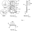
- an optical waveguide 10 is shown having a number of features in common with the prior art waveguide described above with reference to Figures 4 and 5 and shown in WO201 0/11119240 , the contents of which patent publication are hereby incorporated by reference.
- the description of the present embodiment will concentrate predominantly on the inventive differences between the prior art waveguide shown in figures 4 and 5 and that of the present invention, in particular the arrangement of the turning diffraction region (region 48 in Figure 4 ),
- the waveguide 10 comprises an input diffraction region 11 for coupling an input pupil 12 of image-bearing light into the waveguide 10 for propagation by total internal reflection,
- the input pupil 12 is directed towards a reflective surface 13. in this example, where it is reflected towards a turning diffraction region 14.
- the turning diffraction region 14 expands the pupil of image-bearing light in a first dimension 15 through multiple interactions with the region 14 and turns it towards an output diffraction region 16.
- the output diffraction region 16 expands the pupil of image-bearing light in a second dimension 17 and outputs it from the waveguide as an exit pupil 180.
- the reflecting surface 13 may be omitted as described above.
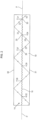
- a section is taken through the waveguide showing a diffraction grating 18 used to implement the turning diffraction region 14 in more detail.
- the profile of the grating 18 is arranged to present the same profile to light approaching the grating 18 from any given angle either above or below the plane P of the waveguide,
- the profile of the grating 18 may for example be a square-wave profile as shown in Figures 2 , or a sinusoidal or triangular profile.
- Such regular, periodic grating profiles share the property of being symmetric about a plane normal to the plane P of the waveguide 10. However, the periodicity of the profile may be varied across the grating 18 while still retaining the property of presenting the same profile to light approaching the grating 18 from a given angle either above or below the plane P of the waveguide,
- the grating 18 is embedded within the waveguide 10, unlike in the prior art waveguide of Figure 4 and Figure 5 in which the gratings are formed on a surface of the waveguide,
- the grating 18 may extend in any plane P of the waveguide 10 although, in the present exarnple it is off-set from a plane which is equally spaced between the principal surfaces 30, 31 of the waveguide 10. The off-set is sufficient to improve pupil banding and uniformity.
- the embedded arrangement of the grating 18 results a greater number of interactions between the light and the grating 18 than would be possible with a surface-formed grating.
- a chief input ray 19 is directed towards the grating 18 of the turning diffraction region 14 from the input diffraction region 11 (not shown in Figure 2 ), whether or not via a reflecting surface 13.
- the input ray 19 has a first angle of polarisation.
- a portion 21 of the light is directed towards the output diffraction region 16 (not shown in Figure 2 ) and a portion 22 of the light continues to propagate along the grating 18.
- the angle of polarisation of both the portions 21, 22 is rotated in one direction, for example a clockwise direction, and therefore the angles of polarisation of light rays 21, 22 are different from that of the input ray 19.
- a portion 24 of the propagating ray 22 is directed towards the output diffraction region 16 and a portion 25 of the light continues to propagate along the grating 18.
- the angle of polarisation of both the portions 24, 25 is rotated in an opposite direction, for example an anti-clockwise direction.
- the second interaction 23 causes the angle of polarisation of the light to be rotated by an equal and opposite amount to the rotation caused by the first interaction 20. Consequently, the angle of polarisation of rays, 24, 25 is typically the same or substantially the same as the angle of polarisation of the input ray 19. Accordingly, the angle of polarisation of the propagating chief ray 25 has therefore returned substantially to the original angle of polarisation of the input ray 19.
- the rays 21, 27, 28 diffracted towards the output region 16 have a generally uniform first angle of polarisation and the rays 24, 29, 32 diffracted towards the output region 16 have a generally uniform second angle of polarisation.
- the output diffraction region 16 is sensitive to polarisation and therefore will typically diffract one set of rays (either the odd rays 21, 27, 28 or the even rays 24, 29, 32) more efficiently than the other set of rays,
- the angles of polarisation of the diffracted rays 66, 72, 78 are different from one another
- the angles of polarisation of the even rays are uniform and the angles of polarisation of the odd rays are uniform and therefore the intensity of the image (at least in the X-dimension) output to a viewer will be generally uniform, even though one set of rays is diffracted less efficiently.
- the input diffraction region 11 and the turning diffraction region 14 may be formed by a single grating 33 which is embedded within the waveguide 10.
- a single grating 33 has advantages from a manufacturing perspective in that the grating 33 can be formed in one manufacturing step, enabling the fringes of the input region 11 to be more accurately aligned with respect to the fringes of the turning region 14.
- the input region 11 and the turning region 14 may be formed by separate gratings and in this case the reflective surface 13 is not required.
- this latter arrangement may be preferred if a requirement of the optical system is that the input region is formed by a surface grating, in a still further arrangement the turning region 14 and the output region 16 may be formed by a single embedded grating and in this case a reflective surface is required and is located on an optical path between the turning region 14 and the output region 16 as described in greater detail in the present applicant's earlier application referenced above,
- the profile of the grating 18 used to implement the turning region 14 may be formed by conventional means which will be apparent to those skilled in the relevant art, for example by etching or by holography.
- a suitable embedded grating can for example be created as described in the present applicant's earlier patent application WO 2010/122330 .
- a suitable profile would be created on the surface of a glass substrate by optical replication from a suitable master profile.
- the surface would be coated with at least one layer of dielectric material such as titanium dioxide, silicon dioxide or magnesium oxide.
- a second glass substrate would then be laminated over the coated surface using a suitable optical adhesive.
- One example design would use N-BK7 glass and a cement of matching refractive index, a square wave grating profile of 435nm period and 50nm depth with a titanium dioxide coating of between 25nm and 50nm thickness.
- the optical waveguide 10 described with reference to Figures 1 and 2 may form part of head-up display, a head or helmet mounted display or other display device.
- a helmet mounted display 34 is shown in Figure 3 mounted to a helmet 35 worn by a viewer 36.
- a light source 37 illuminates a micro projector 38 for injecting image bearing light into the waveguide 10 in accordance with image data supplied by an image processor 39.
- An image is propagated through the waveguide 10 and diffracted out to the user's eye as a visible image 180 with uniform intensity.
Landscapes
- Physics & Mathematics (AREA)
- General Physics & Mathematics (AREA)
- Optics & Photonics (AREA)
- Diffracting Gratings Or Hologram Optical Elements (AREA)
- Optical Couplings Of Light Guides (AREA)
Abstract
Description
- This invention relates to an optical waveguide and a display device. In particular it is relevant to display devices in which image bearing light is injected into a waveguide, is expanded in two orthogonal dimensions to form a visible image and is released from the waveguide.
- A known form of waveguide for use in a display device has been described in an earlier international patent application by the present Applicant, published as
WO 2010/119240 , as will now be described with reference toFigure 4 , The waveguide in that case comprises aninput diffraction region 42 for coupling aninput pupil 44 of image-bearing light into the waveguide for propagation by total internal reflection. Theinput pupil 44 is directed towards areflective surface 46 where it is reflected towards aturning diffraction region 48. The turningdiffraction region 48 expands the pupil in afirst dimension 50 through multiple interactions with theregion 48 and turns it towards anoutput diffraction region 52, Theoutput diffraction region 52 expands the pupil in asecond dimension 54 and outputs the image-bearing light from the waveguide with anexit pupil 56, The use of thereflecting surface 46 allows theinput diffraction region 42 and the turningdiffraction region 48 to be formed by asingle grating 58, Tile reflectingsurface 46 may be omitted, although in that case each of the diffraction regions will be formed by separate gratings. - The orientation of the grooves of the
grating 58 are inclined at an angle of 60° to the x-axis so that image-bearing light incident on theinput region 42 is diffracted and propagated to thereflective surface 46 and thence reflected so that the chief ray propagates and is incident on the grooves of the turningregion 48 at 60° to the normal to the grooves (see inset A), The light is partially diffracted and expanded in a first dimension (here the x-dimension) and propagates through the waveguide to the output low diffraction efficiency (2% to 20%) grating 52 having its orientation (grooves) lying in the x-direction. The diffracted rays are incident normally on this grating (see inset B) and are partially diffracted out of the waveguide, the partial diffraction expanding the pupil in a second dimension, here the y-dimension, resulting in theexit pupil 56, - Typical implementations of the waveguide designs described above use a
grating blazed grating profile 60 as used for the turningregion 48 in the earlier patent application, shown inFigure 5 , to optimise the diffraction efficiency. Analysis has shown that the angledturning diffraction region 48, as required to direct the light towards theoutput diffraction region 52, will typically rotate the polarisation of both the diffracted light directed towards theoutput diffraction region 52 and also the light which continues to propagate making multiple further interactions to expand the input pupil in one dimension, - Referring to
Figure 5 , achief input ray 62 is shown directed towards the turningdiffraction region 48 from the input diffraction region 42 (not shown inFigure 5 ), whether or not via a reflectingsurface 46. Theinput ray 62 has a first angle of polarisation, that is, changes to the state of polarisation of the light may be identified with reference to an angle associated with the state of polarisation of theinput ray 62 even though the light is not necessarily plans-polarised. At afirst interaction 64 with theturning region 48, aportion 66 of the light is directed towards the output diffraction region 52 (not shown inFigure 5 ) and aportion 68 of the light continues to propagate along theturning region 48, At thefirst interaction 64, the angle of polarisation of both of theportions light rays input ray 62. At asecond interaction 70 with thegrating 48, aportion 72 of the propagatingray 68 is directed towards theoutput diffraction region 52 and aportion 74 of the light continues to propagate along the turningregion 48, At thesecond interaction 70, the angle of polarisation of both theportions input ray 62 and the propagatingray 68, At athird interaction 76 with thegrating 48, aportion 78 of the propagatingray 74 is directed towards theoutput diffraction region 52 and a portion 80 of the light continues to propagate along the turning region, At thethird interaction 76, the angle of polarisation of both theportions 78, 80 are rotated further in the same direction, for example a clockwise direction. Consequently, the angle of polarisation of therays 78, 80 are typically different from the angles of polarisation of theinput ray 62, the propagatingray 68 and the propagatingray 74. Multiple further interactions will occur between propagating rays and thegrating 48, although only three interactions are shown. Accordingly, the angles of polarisation of therays output diffraction region 52 are typically different from each other. In the example shown inFigure 4 , theoutput diffraction region 52 is sensitive to the polarisation of light such that a ray having one angle of polarisation will be more optimally diffracted towards a viewer than a ray having another angle of polarisation. Therays exit pupil 56 as light is output from the waveguide at different intensities producing lighter and darker regions. - The present invention provides optical waveguide in which, in operation, image-bearing light propagates therein by total internal reflection, the waveguide comprising at least first and second diffraction regions, the first diffraction region being arranged to diffract image-bearing light propagating along the waveguide so as to expand it in a first dimension and to turn the image-bearing light towards the second diffraction region, the second diffraction region being arranged to diffract the image-bearing light so as to expand it in a second dimension and to release it from the waveguide as a visible image wherein the first diffraction region is formed by first diffraction grating embedded within the waveguide, arranged to present a substantially similar profile to the image-bearing light when incident upon the grating from a given angle above or below the grating such that the polarisation of the image bearing light is rotated by substantially similar amounts, but in opposite directions, by successive interactions with the first diffraction region, thereby increasing the uniformity of intensity of the visible image released from the waveguide.
- The image bearing light turned towards the second diffraction region following an even number of interactions with the first diffraction region may have substantially the same polarisation. Additionally or alternatively, the image bearing light turned towards the second diffraction region following an odd number of interactions with the first diffraction region may have substantially the same polarisation.
- The grating profile may be symmetrical with respect to a plane extending normally to the waveguide and spaced from a first and from a second principle surfaces of the waveguide by different amounts,
- The first diffraction region may have a periodic square wave, sinusoidal or triangular profile.
- The invention also provides a helmet-mounted, head-mounted, head-up or other display device comprising such an optical waveguide.
- The invention now will be described merely by way of example with reference to the accompanying drawings wherein;
-
Figure 1 shows an optical waveguide; -
Figure 2 shows a diffraction region of the optical waveguide; -
Figure 3 shows a display device comprising the optical waveguide; -
Figure 4 shows a prior art optical waveguide; and -
Figure 5 shows a diffraction region of the prior art waveguide, - Referring to
Figures 1 and2 , anoptical waveguide 10 is shown having a number of features in common with the prior art waveguide described above with reference toFigures 4 and5 and shown inWO201 0/11119240 figures 4 and5 and that of the present invention, in particular the arrangement of the turning diffraction region (region 48 inFigure 4 ), - The
waveguide 10 comprises aninput diffraction region 11 for coupling aninput pupil 12 of image-bearing light into thewaveguide 10 for propagation by total internal reflection, Theinput pupil 12 is directed towards areflective surface 13. in this example, where it is reflected towards aturning diffraction region 14. The turningdiffraction region 14 expands the pupil of image-bearing light in afirst dimension 15 through multiple interactions with theregion 14 and turns it towards anoutput diffraction region 16. Theoutput diffraction region 16 expands the pupil of image-bearing light in asecond dimension 17 and outputs it from the waveguide as anexit pupil 180. The reflectingsurface 13 may be omitted as described above. - in
Figure 2 , a section is taken through the waveguide showing a diffraction grating 18 used to implement the turningdiffraction region 14 in more detail. The profile of thegrating 18 is arranged to present the same profile to light approaching thegrating 18 from any given angle either above or below the plane P of the waveguide, The profile of thegrating 18 may for example be a square-wave profile as shown inFigures 2 , or a sinusoidal or triangular profile. Such regular, periodic grating profiles share the property of being symmetric about a plane normal to the plane P of thewaveguide 10. However, the periodicity of the profile may be varied across thegrating 18 while still retaining the property of presenting the same profile to light approaching thegrating 18 from a given angle either above or below the plane P of the waveguide, - The
grating 18 is embedded within thewaveguide 10, unlike in the prior art waveguide ofFigure 4 andFigure 5 in which the gratings are formed on a surface of the waveguide, Thegrating 18 may extend in any plane P of thewaveguide 10 although, in the present exarnple it is off-set from a plane which is equally spaced between theprincipal surfaces waveguide 10. The off-set is sufficient to improve pupil banding and uniformity. The embedded arrangement of thegrating 18 results a greater number of interactions between the light and thegrating 18 than would be possible with a surface-formed grating. - A
chief input ray 19 is directed towards thegrating 18 of the turningdiffraction region 14 from the input diffraction region 11 (not shown inFigure 2 ), whether or not via a reflectingsurface 13. Theinput ray 19 has a first angle of polarisation. At afirst interaction 20 with thegrating 18, aportion 21 of the light is directed towards the output diffraction region 16 (not shown inFigure 2 ) and aportion 22 of the light continues to propagate along thegrating 18. At thefirst interaction 20, the angle of polarisation of both theportions light rays input ray 19. - At a
second interaction 23 with thegrating 18, aportion 24 of the propagatingray 22 is directed towards theoutput diffraction region 16 and aportion 25 of the light continues to propagate along thegrating 18. At thesecond interaction 23, the angle of polarisation of both theportions second interaction 23 causes the angle of polarisation of the light to be rotated by an equal and opposite amount to the rotation caused by thefirst interaction 20. Consequently, the angle of polarisation of rays, 24, 25 is typically the same or substantially the same as the angle of polarisation of theinput ray 19. Accordingly, the angle of polarisation of the propagatingchief ray 25 has therefore returned substantially to the original angle of polarisation of theinput ray 19. - It will be seen therefore that successive interactions with the
grating 18 cause opposite rotation of the angle of polarisation of both the diffracted rays and the propagating rays, In this way, after an odd number of interactions with the turning grating 18 the angles of polarisation of the diffracted light and the propagating light are rotated compared to the angle of polarisation of theinput ray 19 and after an even number of interactions with the turning grating 18 the angles of polarisation of the diffracted light and the propagating light are generally similar or the same as the angle of polarisation of theinput ray 19. That is, therays output region 16 have a generally uniform first angle of polarisation and therays output region 16 have a generally uniform second angle of polarisation. Theoutput diffraction region 16 is sensitive to polarisation and therefore will typically diffract one set of rays (either theodd rays even rays diffracted rays - It should further be noted that the chief rays of the arrangement have been described in relation to
Figures 1 and2 . Thechief rays Figure 1 extending across theX-dimension 15, On first appearance therefore it would seem that the difference in polarisation of the odd and even rays would give rise to banding due to differing diffraction efficiency of theoutput region 18. However, it must be appreciated that in addition to the chief rays there will be dispersion of light such that rays diffracted from the turning grating will tend to overlap and eliminate any banding. - Referring to
Figure 1 , theinput diffraction region 11 and the turningdiffraction region 14 may be formed by asingle grating 33 which is embedded within thewaveguide 10. Asingle grating 33 has advantages from a manufacturing perspective in that thegrating 33 can be formed in one manufacturing step, enabling the fringes of theinput region 11 to be more accurately aligned with respect to the fringes of the turningregion 14. Alternatively, theinput region 11 and the turningregion 14 may be formed by separate gratings and in this case thereflective surface 13 is not required. For example, this latter arrangement may be preferred if a requirement of the optical system is that the input region is formed by a surface grating, in a still further arrangement the turningregion 14 and theoutput region 16 may be formed by a single embedded grating and in this case a reflective surface is required and is located on an optical path between the turningregion 14 and theoutput region 16 as described in greater detail in the present applicant's earlier application referenced above, - The profile of the
grating 18 used to implement the turningregion 14 may be formed by conventional means which will be apparent to those skilled in the relevant art, for example by etching or by holography. - A suitable embedded grating can for example be created as described in the present applicant's earlier patent application
WO 2010/122330 . In one example a suitable profile would be created on the surface of a glass substrate by optical replication from a suitable master profile. The surface would be coated with at least one layer of dielectric material such as titanium dioxide, silicon dioxide or magnesium oxide. A second glass substrate would then be laminated over the coated surface using a suitable optical adhesive. One example design would use N-BK7 glass and a cement of matching refractive index, a square wave grating profile of 435nm period and 50nm depth with a titanium dioxide coating of between 25nm and 50nm thickness. - The
optical waveguide 10 described with reference toFigures 1 and2 may form part of head-up display, a head or helmet mounted display or other display device. By way of example, a helmet mounteddisplay 34 is shown inFigure 3 mounted to ahelmet 35 worn by aviewer 36. Alight source 37 illuminates amicro projector 38 for injecting image bearing light into thewaveguide 10 in accordance with image data supplied by animage processor 39. An image is propagated through thewaveguide 10 and diffracted out to the user's eye as avisible image 180 with uniform intensity. - Further exemplary embodiments of the present disclosure are set out in the following numbered clauses:
- Clause 1. An optical waveguide in which, in operation, image-bearing light propagates therein by total internal reflection, the waveguide comprising at least first and second diffraction regions, the first diffraction region being arranged to diffract image-bearing light propagating along the waveguide so as to expand it in a first dimension and to turn the image-bearing light towards the second diffraction region, the second diffraction region being arranged to diffract the image-bearing light so as to expand it in a second dimension and to release it from the waveguide as a visible image, wherein the first diffraction region is formed by first diffraction grating embedded within the waveguide, arranged to present a substantially similar profile to the image-bearing light when incident upon the grating from a given angle above or below the grating such that the polarization of the image bearing light is rotated by substantially similar amounts, but in opposite directions by successive interactions with the first diffraction region, there increasing the uniformity of intensity of the visible image released from the waveguide.
- Clause 2. The waveguide according to clause 1, wherein the image bearing light, when turned towards the second diffraction region following an even number of interactions with the first diffraction region has substantially the same polarisation and/or the image bearing light, when turned towards the second diffraction region following an odd number of interactions with the first diffraction region has substantially the same polarisation.
- Clause 3. The waveguide according to clause 1 or clause 2, wherein the profile of the first diffraction grating is substantially symmetrical about a plane extending normally to the waveguide and wherein the first diffraction grating is spaced from a first and from a second principle surface of the waveguide by different amounts.
- Clause 4. The waveguide according to any one of the preceding clauses, wherein the first diffraction grating has a periodic square wave, sinusoidal or triangular profile.
- Clause 5. An optical waveguide substantially as herein described with reference to and as shown in
Figure 1 andFigure 2 of the accompanying drawings. - Clause 6. A helmet-mounted, head-mounted, head-up or other display device comprising the waveguide of any preceding clause.
Claims (12)
- A display device, comprising:an optical waveguide; anda diffraction grating embedded within the optical waveguide, the diffraction grating configured to cause a first angle of polarization of light interacting with the diffraction grating from below the diffraction grating to rotate in a first direction and by a first amount, the diffraction grating further configured to cause a second angle of polarization of light interacting with the diffraction grating from above the diffraction grating to rotate in a second direction opposite to the first direction and by a second amount approximately equal to the first amount, such that the polarization of the light is substantially unchanged after the light has interacted with the diffraction grating from below the diffraction grating and subsequently from above the diffraction grating via total internal reflection within the optical waveguide.
- The display device of claim 1, wherein the optical waveguide includes at least a first diffraction region and a second diffraction region.
- The display device of claim 2, wherein, in operation, the first diffraction region is arranged to diffract image-bearing light propagating along the optical waveguide so as to expand the image-bearing light in a first dimension and to turn the image-bearing light towards the second diffraction region, the second diffraction region being arranged to diffract the image-bearing light so as to expand it in a second dimension and to release it from the optical waveguide as a visible image.
- The display device of any one of the preceding claims, wherein, in operation, the diffraction grating is configured such that, after an odd number of interactions with the diffraction grating, an angle of polarization of light within the optical waveguide is rotated compared to an angle of polarization of an input ray, and after an even number of interactions with the diffraction grating, the angle of polarization of the light within the optical waveguide is approximately the same as the angle of polarization of the input ray.
- The display device of any one of claim 2 to claim 4, wherein a profile of the first diffraction region is substantially symmetrical about a plane extending normally to the optical waveguide, the first diffraction region being spaced from a first principal surface and from a second principal surface of the optical waveguide by different amounts.
- The display device of any one of claim 2 to claim 5, wherein the first diffraction region has a profile that is one of a periodic square profile, a sinusoidal profile, and a triangular profile.
- The display device of any one of claim 2 to claim 6, wherein a cross-section of a profile of the first diffraction region is periodic.
- The display device of any one of claim 2 to claim 7, wherein, in operation, at each successive interaction with a successive portion of the image-bearing light with the first diffraction region, the first diffraction region is configured to:
diffract a further portion of the successive portion such that a polarization angle of one of the further portions is rotated relative to a plane of the optical waveguide to direct the further portion toward the second diffraction region, and diffract another further portion of the successive portion such that a polarization angle of the another further portion is rotated relative to the plane of the optical waveguide to propagate the another further portion along the first diffraction region. - The display device of any one of claim 2 to claim 8, wherein the first diffraction region further comprises an input-diffraction region to couple an input pupil of the image-bearing light into the optical waveguide.
- The display device of claim 9, further comprising a reflective surface configured to reflect the input pupil towards the diffraction grating.
- The display device of any one of the preceding claims, wherein the diffraction grating is configured to present a similar profile to light interacting with the diffraction grating from below the diffraction grating as to light interacting with the diffraction grating from above the diffraction grating.
- The display device of any one of any one of the preceding claims, wherein the display device is configured to be mounted to one of a helmet, a head-mounted device, a head-up device, and any other device.
Applications Claiming Priority (3)
| Application Number | Priority Date | Filing Date | Title |
|---|---|---|---|
| GBGB1117029.7A GB201117029D0 (en) | 2011-10-04 | 2011-10-04 | Optical waveguide and display device |
| EP12778777.8A EP2764394B1 (en) | 2011-10-04 | 2012-10-04 | Optical waveguide and display device |
| PCT/GB2012/052453 WO2013050762A1 (en) | 2011-10-04 | 2012-10-04 | Optical waveguide and display device |
Related Parent Applications (1)
| Application Number | Title | Priority Date | Filing Date |
|---|---|---|---|
| EP12778777.8A Division EP2764394B1 (en) | 2011-10-04 | 2012-10-04 | Optical waveguide and display device |
Publications (2)
| Publication Number | Publication Date |
|---|---|
| EP4553564A2 true EP4553564A2 (en) | 2025-05-14 |
| EP4553564A3 EP4553564A3 (en) | 2025-07-16 |
Family
ID=45035067
Family Applications (2)
| Application Number | Title | Priority Date | Filing Date |
|---|---|---|---|
| EP25166607.9A Pending EP4553564A3 (en) | 2011-10-04 | 2012-10-04 | Optical waveguide and display device |
| EP12778777.8A Active EP2764394B1 (en) | 2011-10-04 | 2012-10-04 | Optical waveguide and display device |
Family Applications After (1)
| Application Number | Title | Priority Date | Filing Date |
|---|---|---|---|
| EP12778777.8A Active EP2764394B1 (en) | 2011-10-04 | 2012-10-04 | Optical waveguide and display device |
Country Status (7)
| Country | Link |
|---|---|
| US (1) | US10088633B2 (en) |
| EP (2) | EP4553564A3 (en) |
| CN (1) | CN103959133B (en) |
| AU (1) | AU2012320305B2 (en) |
| CA (1) | CA2850948C (en) |
| GB (2) | GB201117029D0 (en) |
| WO (1) | WO2013050762A1 (en) |
Families Citing this family (110)
| Publication number | Priority date | Publication date | Assignee | Title |
|---|---|---|---|---|
| IL166799A (en) | 2005-02-10 | 2014-09-30 | Lumus Ltd | Substrate-guided optical device utilizing beam splitters |
| US10073264B2 (en) | 2007-08-03 | 2018-09-11 | Lumus Ltd. | Substrate-guide optical device |
| GB0522968D0 (en) | 2005-11-11 | 2005-12-21 | Popovich Milan M | Holographic illumination device |
| GB0718706D0 (en) | 2007-09-25 | 2007-11-07 | Creative Physics Ltd | Method and apparatus for reducing laser speckle |
| US9335604B2 (en) | 2013-12-11 | 2016-05-10 | Milan Momcilo Popovich | Holographic waveguide display |
| US11726332B2 (en) | 2009-04-27 | 2023-08-15 | Digilens Inc. | Diffractive projection apparatus |
| US11204540B2 (en) | 2009-10-09 | 2021-12-21 | Digilens Inc. | Diffractive waveguide providing a retinal image |
| WO2011042711A2 (en) | 2009-10-09 | 2011-04-14 | Milan Momcilo Popovich | Compact edge illuminated diffractive display |
| US9274349B2 (en) | 2011-04-07 | 2016-03-01 | Digilens Inc. | Laser despeckler based on angular diversity |
| US10670876B2 (en) | 2011-08-24 | 2020-06-02 | Digilens Inc. | Waveguide laser illuminator incorporating a despeckler |
| EP2995986B1 (en) | 2011-08-24 | 2017-04-12 | Rockwell Collins, Inc. | Data display |
| WO2016020630A2 (en) | 2014-08-08 | 2016-02-11 | Milan Momcilo Popovich | Waveguide laser illuminator incorporating a despeckler |
| GB201117029D0 (en) | 2011-10-04 | 2011-11-16 | Bae Systems Plc | Optical waveguide and display device |
| CN108508523B (en) * | 2017-02-24 | 2020-09-01 | 北京耐德佳显示技术有限公司 | Waveguide type optical element and near-to-eye display device using same |
| WO2013102759A2 (en) | 2012-01-06 | 2013-07-11 | Milan Momcilo Popovich | Contact image sensor using switchable bragg gratings |
| WO2013163347A1 (en) | 2012-04-25 | 2013-10-31 | Rockwell Collins, Inc. | Holographic wide angle display |
| US9456744B2 (en) | 2012-05-11 | 2016-10-04 | Digilens, Inc. | Apparatus for eye tracking |
| US9933684B2 (en) | 2012-11-16 | 2018-04-03 | Rockwell Collins, Inc. | Transparent waveguide display providing upper and lower fields of view having a specific light output aperture configuration |
| WO2014188149A1 (en) | 2013-05-20 | 2014-11-27 | Milan Momcilo Popovich | Holographic waveguide eye tracker |
| US9727772B2 (en) | 2013-07-31 | 2017-08-08 | Digilens, Inc. | Method and apparatus for contact image sensing |
| CN106030376B (en) | 2013-12-19 | 2019-06-07 | Bae系统公共有限公司 | In waveguide and relevant improvement |
| GB201322488D0 (en) * | 2013-12-19 | 2014-02-05 | Bae Systems Plc | Improvements in and relating to waveguides |
| EP3084509B1 (en) | 2013-12-19 | 2018-10-03 | BAE Systems PLC | Improvements in and relating to waveguides |
| IL232197B (en) | 2014-04-23 | 2018-04-30 | Lumus Ltd | Compact head-mounted display system |
| US10359736B2 (en) | 2014-08-08 | 2019-07-23 | Digilens Inc. | Method for holographic mastering and replication |
| US10241330B2 (en) | 2014-09-19 | 2019-03-26 | Digilens, Inc. | Method and apparatus for generating input images for holographic waveguide displays |
| EP3198192A1 (en) | 2014-09-26 | 2017-08-02 | Milan Momcilo Popovich | Holographic waveguide opticaltracker |
| IL235642B (en) | 2014-11-11 | 2021-08-31 | Lumus Ltd | Compact head-mounted display system protected by a hyperfine structure |
| EP3245444B1 (en) | 2015-01-12 | 2021-09-08 | DigiLens Inc. | Environmentally isolated waveguide display |
| WO2016113533A2 (en) | 2015-01-12 | 2016-07-21 | Milan Momcilo Popovich | Holographic waveguide light field displays |
| WO2016116733A1 (en) | 2015-01-20 | 2016-07-28 | Milan Momcilo Popovich | Holographic waveguide lidar |
| US9632226B2 (en) | 2015-02-12 | 2017-04-25 | Digilens Inc. | Waveguide grating device |
| WO2016146963A1 (en) | 2015-03-16 | 2016-09-22 | Popovich, Milan, Momcilo | Waveguide device incorporating a light pipe |
| CN107530034A (en) | 2015-03-16 | 2018-01-02 | 奇跃公司 | Augmented reality pulse oximetry |
| US10591756B2 (en) | 2015-03-31 | 2020-03-17 | Digilens Inc. | Method and apparatus for contact image sensing |
| US9910276B2 (en) | 2015-06-30 | 2018-03-06 | Microsoft Technology Licensing, Llc | Diffractive optical elements with graded edges |
| US10670862B2 (en) | 2015-07-02 | 2020-06-02 | Microsoft Technology Licensing, Llc | Diffractive optical elements with asymmetric profiles |
| US10038840B2 (en) | 2015-07-30 | 2018-07-31 | Microsoft Technology Licensing, Llc | Diffractive optical element using crossed grating for pupil expansion |
| US9864208B2 (en) | 2015-07-30 | 2018-01-09 | Microsoft Technology Licensing, Llc | Diffractive optical elements with varying direction for depth modulation |
| US10073278B2 (en) | 2015-08-27 | 2018-09-11 | Microsoft Technology Licensing, Llc | Diffractive optical element using polarization rotation grating for in-coupling |
| CN113759555B (en) | 2015-10-05 | 2024-09-20 | 迪吉伦斯公司 | Waveguide Display |
| US10429645B2 (en) | 2015-10-07 | 2019-10-01 | Microsoft Technology Licensing, Llc | Diffractive optical element with integrated in-coupling, exit pupil expansion, and out-coupling |
| US10241332B2 (en) | 2015-10-08 | 2019-03-26 | Microsoft Technology Licensing, Llc | Reducing stray light transmission in near eye display using resonant grating filter |
| US9946072B2 (en) | 2015-10-29 | 2018-04-17 | Microsoft Technology Licensing, Llc | Diffractive optical element with uncoupled grating structures |
| US10359627B2 (en) * | 2015-11-10 | 2019-07-23 | Microsoft Technology Licensing, Llc | Waveguide coatings or substrates to improve intensity distributions having adjacent planar optical component separate from an input, output, or intermediate coupler |
| US10234686B2 (en) | 2015-11-16 | 2019-03-19 | Microsoft Technology Licensing, Llc | Rainbow removal in near-eye display using polarization-sensitive grating |
| AU2016355125A1 (en) | 2015-11-20 | 2018-07-05 | David Long | Power manager with reconfigurable power converting circuits |
| US11258366B2 (en) | 2015-11-20 | 2022-02-22 | Galvion Soldier Power, Llc | Power manager with reconfigurable power converting circuits |
| US10983340B2 (en) | 2016-02-04 | 2021-04-20 | Digilens Inc. | Holographic waveguide optical tracker |
| WO2017162999A1 (en) | 2016-03-24 | 2017-09-28 | Popovich Milan Momcilo | Method and apparatus for providing a polarization selective holographic waveguide device |
| EP4273615B1 (en) | 2016-04-08 | 2025-11-12 | Magic Leap, Inc. | Augmented reality systems and methods with variable focus lens elements |
| US10890707B2 (en) | 2016-04-11 | 2021-01-12 | Digilens Inc. | Holographic waveguide apparatus for structured light projection |
| US10067347B2 (en) * | 2016-04-13 | 2018-09-04 | Microsoft Technology Licensing, Llc | Waveguides with improved intensity distributions |
| US10095045B2 (en) * | 2016-09-12 | 2018-10-09 | Microsoft Technology Licensing, Llc | Waveguide comprising a bragg polarization grating |
| JP7187022B2 (en) | 2016-10-09 | 2022-12-12 | ルムス エルティーディー. | Aperture multiplier using rectangular waveguide |
| KR102541662B1 (en) | 2016-11-08 | 2023-06-13 | 루머스 리미티드 | Light-guide device with optical cutoff edge and corresponding production methods |
| EP3548939A4 (en) | 2016-12-02 | 2020-11-25 | DigiLens Inc. | WAVE GUIDE DEVICE WITH UNIFORM OUTPUT LIGHTING |
| US20190377187A1 (en) * | 2017-01-04 | 2019-12-12 | Lumus Ltd. | Optical system for near-eye displays |
| WO2018129398A1 (en) | 2017-01-05 | 2018-07-12 | Digilens, Inc. | Wearable heads up displays |
| US10108014B2 (en) * | 2017-01-10 | 2018-10-23 | Microsoft Technology Licensing, Llc | Waveguide display with multiple focal depths |
| US10698214B2 (en) * | 2017-01-17 | 2020-06-30 | Microsoft Technology Licensing, Llc | Optical device to improve image uniformity |
| WO2018138714A1 (en) | 2017-01-28 | 2018-08-02 | Lumus Ltd. | Augmented reality imaging system |
| KR102601052B1 (en) | 2017-02-23 | 2023-11-09 | 매직 립, 인코포레이티드 | Display system with variable power reflector |
| TWI800974B (en) | 2017-03-22 | 2023-05-01 | 以色列商魯姆斯有限公司 | A method for producing a light-guide optical element |
| US10281726B2 (en) | 2017-04-04 | 2019-05-07 | Microsoft Technology Licensing, Llc | Refractive-diffractive display system with wide field of view |
| US10942430B2 (en) | 2017-10-16 | 2021-03-09 | Digilens Inc. | Systems and methods for multiplying the image resolution of a pixelated display |
| FI129586B (en) | 2017-12-22 | 2022-05-13 | Dispelix Oy | Multipupil waveguide display element and display device |
| MX2020002402A (en) | 2018-01-02 | 2020-07-22 | Lumus Ltd | AUGMENTED REALITY SCREENS WITH ACTIVE ALIGNMENT AND CORRESPONDING METHODS. |
| US10732569B2 (en) | 2018-01-08 | 2020-08-04 | Digilens Inc. | Systems and methods for high-throughput recording of holographic gratings in waveguide cells |
| US20190212588A1 (en) | 2018-01-08 | 2019-07-11 | Digilens, Inc. | Systems and Methods for Manufacturing Waveguide Cells |
| KR20250004154A (en) | 2018-01-08 | 2025-01-07 | 디지렌즈 인코포레이티드. | Methods for fabricating optical waveguides |
| US10914950B2 (en) | 2018-01-08 | 2021-02-09 | Digilens Inc. | Waveguide architectures and related methods of manufacturing |
| CN112088332B (en) | 2018-03-16 | 2024-11-29 | 迪吉伦斯公司 | Holographic waveguides comprising birefringence control and methods for their manufacture |
| IL259518B2 (en) | 2018-05-22 | 2023-04-01 | Lumus Ltd | Optical system and method for improvement of light field uniformity |
| US11415812B2 (en) | 2018-06-26 | 2022-08-16 | Lumus Ltd. | Compact collimating optical device and system |
| WO2020023779A1 (en) | 2018-07-25 | 2020-01-30 | Digilens Inc. | Systems and methods for fabricating a multilayer optical structure |
| KR102848817B1 (en) | 2018-11-08 | 2025-08-20 | 삼성전자주식회사 | backlight unit and holographic display apparatus including the same |
| WO2020149956A1 (en) | 2019-01-14 | 2020-07-23 | Digilens Inc. | Holographic waveguide display with light control layer |
| US20200247017A1 (en) | 2019-02-05 | 2020-08-06 | Digilens Inc. | Methods for Compensating for Optical Surface Nonuniformity |
| US20220283377A1 (en) | 2019-02-15 | 2022-09-08 | Digilens Inc. | Wide Angle Waveguide Display |
| CN113692544B (en) | 2019-02-15 | 2025-04-22 | 迪吉伦斯公司 | Method and apparatus for providing holographic waveguide displays using integrated gratings |
| CN113474715A (en) | 2019-02-28 | 2021-10-01 | 鲁姆斯有限公司 | Compact collimated image projector |
| KR102651647B1 (en) | 2019-03-12 | 2024-03-26 | 루머스 리미티드 | image projector |
| US20200292745A1 (en) | 2019-03-12 | 2020-09-17 | Digilens Inc. | Holographic Waveguide Backlight and Related Methods of Manufacturing |
| JP3237907U (en) | 2019-04-04 | 2022-06-16 | ルムス エルティーディー. | Vertical near-eye display with no air gap |
| TWI916247B (en) | 2019-04-15 | 2026-02-21 | 以色列商魯姆斯有限公司 | Light-guide optical element |
| CN114207492A (en) | 2019-06-07 | 2022-03-18 | 迪吉伦斯公司 | Waveguide with transmission grating and reflection grating and method for producing the same |
| JP7514558B2 (en) | 2019-07-04 | 2024-07-11 | ルーマス リミテッド | Image waveguide with symmetric beam multiplication. |
| US11681143B2 (en) | 2019-07-29 | 2023-06-20 | Digilens Inc. | Methods and apparatus for multiplying the image resolution and field-of-view of a pixelated display |
| KR102775783B1 (en) | 2019-08-29 | 2025-02-28 | 디지렌즈 인코포레이티드. | Vacuum grid and method for manufacturing the same |
| KR20250172729A (en) | 2019-09-16 | 2025-12-09 | 루머스 리미티드 | Compact projector for head-mounted displays |
| JP7396738B2 (en) | 2019-12-05 | 2023-12-12 | ルーマス リミテッド | Light-guiding optics with complementary coating partial reflectors and light-guiding optics with reduced light scattering |
| JP7497079B2 (en) | 2019-12-08 | 2024-06-10 | ルーマス リミテッド | Optical system with a compact image projector |
| CA3167174A1 (en) | 2020-02-06 | 2021-09-23 | Christopher Moore | Rugged integrated helmet vision system |
| TWI718054B (en) | 2020-04-23 | 2021-02-01 | 宏碁股份有限公司 | Optical device combining spectacle function with augmented reality function and augmented reality device |
| JP3243058U (en) | 2020-05-12 | 2023-08-03 | ルムス エルティーディー. | rotary light pipe |
| CN113703173B (en) * | 2020-05-20 | 2023-08-15 | 宏碁股份有限公司 | Optical device and augmented reality device combining glasses function and augmented reality function |
| JP2024502255A (en) | 2020-12-21 | 2024-01-18 | ディジレンズ インコーポレイテッド | Eye glow suppression in waveguide-based displays |
| CN112630967B (en) * | 2020-12-23 | 2022-12-13 | 业成科技(成都)有限公司 | Optical waveguide module and electronic equipment |
| WO2022150841A1 (en) | 2021-01-07 | 2022-07-14 | Digilens Inc. | Grating structures for color waveguides |
| EP4288831A4 (en) | 2021-03-05 | 2025-01-15 | Digilens Inc. | EVACUATED PERIODIC STRUCTURES AND THEIR MANUFACTURING PROCESSES |
| CA3218744A1 (en) | 2021-05-12 | 2022-11-17 | Elaine Violet CRAIGIE | System for forming a deep drawn helmet and method therefor |
| EP4379450A4 (en) * | 2021-07-30 | 2025-01-29 | Panasonic Intellectual Property Management Co., Ltd. | Optical system and head-up display system provided with same |
| US12155263B2 (en) | 2021-08-06 | 2024-11-26 | Galvion Ltd. | Helmet-mounted power system |
| IL310952A (en) | 2021-08-23 | 2024-04-01 | Lumus Ltd | Methods for manufacturing complex light-guiding optical components with embedded coupling reflectors |
| USD1062615S1 (en) | 2021-12-21 | 2025-02-18 | Galvion Soldier Power, Llc | Power pack |
| WO2023150548A2 (en) | 2022-02-03 | 2023-08-10 | Galvion Ltd. | Reconfigurable helmet |
| US12326707B2 (en) | 2022-05-16 | 2025-06-10 | Galvion Ltd. | Method and system of providing a uniform messaging platform in a heterogeneous environment |
| EP4550026A4 (en) * | 2022-06-29 | 2025-10-08 | Panasonic Ip Man Co Ltd | IMAGE DISPLAY DEVICE AND OPTICAL SYSTEM |
| CN115903122B (en) * | 2023-01-06 | 2023-06-06 | 北京至格科技有限公司 | Grating waveguide device and waveguide system for augmented reality display |
Citations (2)
| Publication number | Priority date | Publication date | Assignee | Title |
|---|---|---|---|---|
| WO2010119240A1 (en) | 2009-04-14 | 2010-10-21 | Bae Systems Plc | Optical waveguide and display device |
| WO2010122330A1 (en) | 2009-04-20 | 2010-10-28 | Bae Systems Plc | Surface relief grating in an optical waveguide having a reflecting surface and dielectric layer conforming to the surface |
Family Cites Families (15)
| Publication number | Priority date | Publication date | Assignee | Title |
|---|---|---|---|---|
| US6580529B1 (en) * | 1998-04-02 | 2003-06-17 | Elop Electro -Optics Industries Ltd. | Holographic optical devices |
| WO2003025633A1 (en) * | 2001-09-13 | 2003-03-27 | Asahi Glass Company, Limited | Diffraction device |
| CN1177245C (en) * | 2003-04-02 | 2004-11-24 | 华中科技大学 | Polarization-Independent Folded Arrayed Waveguide Gratings |
| EP1731943B1 (en) * | 2004-03-29 | 2019-02-13 | Sony Corporation | Optical device and virtual image display device |
| JP4218606B2 (en) * | 2004-07-23 | 2009-02-04 | 沖電気工業株式会社 | Optical waveguide device |
| US7174063B2 (en) * | 2005-03-04 | 2007-02-06 | Lucent Technologies Inc. | Colorless tunable dispersion compensator employing a planar lightwave circuit and a deformable mirror |
| US20080043334A1 (en) * | 2006-08-18 | 2008-02-21 | Mirage Innovations Ltd. | Diffractive optical relay and method for manufacturing the same |
| JP2007219106A (en) * | 2006-02-16 | 2007-08-30 | Konica Minolta Holdings Inc | Optical device for expanding diameter of luminous flux, video display device and head mount display |
| CN101589326B (en) * | 2006-12-28 | 2011-06-29 | 诺基亚公司 | Device for expanding an exit pupil in two dimensions |
| EP2153266B1 (en) * | 2007-06-04 | 2020-03-11 | Magic Leap, Inc. | A diffractive beam expander and a virtual display based on a diffractive beam expander |
| US7583439B2 (en) * | 2007-08-09 | 2009-09-01 | University Of Central Florida Research Foundation, Inc. | Wide-angle and broadband polarization converter |
| EP2329302B1 (en) * | 2008-09-16 | 2019-11-06 | BAE Systems PLC | Improvements in or relating to waveguides |
| EP2196843A1 (en) * | 2008-12-12 | 2010-06-16 | BAE Systems PLC | Improvements in or relating to waveguides |
| GB2494115A (en) * | 2011-08-26 | 2013-03-06 | Bae Systems Plc | Projection display with grating arranged to avoid double images |
| GB201117029D0 (en) | 2011-10-04 | 2011-11-16 | Bae Systems Plc | Optical waveguide and display device |
-
2011
- 2011-10-04 GB GBGB1117029.7A patent/GB201117029D0/en not_active Ceased
-
2012
- 2012-10-04 US US14/349,483 patent/US10088633B2/en active Active
- 2012-10-04 GB GB1217736.6A patent/GB2495398B/en active Active
- 2012-10-04 EP EP25166607.9A patent/EP4553564A3/en active Pending
- 2012-10-04 WO PCT/GB2012/052453 patent/WO2013050762A1/en not_active Ceased
- 2012-10-04 CN CN201280059026.2A patent/CN103959133B/en active Active
- 2012-10-04 EP EP12778777.8A patent/EP2764394B1/en active Active
- 2012-10-04 AU AU2012320305A patent/AU2012320305B2/en active Active
- 2012-10-04 CA CA2850948A patent/CA2850948C/en active Active
Patent Citations (2)
| Publication number | Priority date | Publication date | Assignee | Title |
|---|---|---|---|---|
| WO2010119240A1 (en) | 2009-04-14 | 2010-10-21 | Bae Systems Plc | Optical waveguide and display device |
| WO2010122330A1 (en) | 2009-04-20 | 2010-10-28 | Bae Systems Plc | Surface relief grating in an optical waveguide having a reflecting surface and dielectric layer conforming to the surface |
Also Published As
| Publication number | Publication date |
|---|---|
| WO2013050762A1 (en) | 2013-04-11 |
| GB201217736D0 (en) | 2012-11-14 |
| US20140240834A1 (en) | 2014-08-28 |
| GB201117029D0 (en) | 2011-11-16 |
| CN103959133B (en) | 2017-04-12 |
| US10088633B2 (en) | 2018-10-02 |
| CA2850948C (en) | 2020-03-10 |
| GB2495398A (en) | 2013-04-10 |
| AU2012320305A1 (en) | 2014-04-17 |
| EP2764394B1 (en) | 2025-04-09 |
| EP2764394A1 (en) | 2014-08-13 |
| GB2495398B (en) | 2015-12-23 |
| CN103959133A (en) | 2014-07-30 |
| EP4553564A3 (en) | 2025-07-16 |
| AU2012320305B2 (en) | 2015-02-05 |
| CA2850948A1 (en) | 2013-04-11 |
Similar Documents
| Publication | Publication Date | Title |
|---|---|---|
| US10088633B2 (en) | Optical waveguide and display device | |
| AU2010238336B2 (en) | Optical waveguide and display device | |
| EP2241926A1 (en) | Optical waveguide and display device | |
| KR102123896B1 (en) | Near-to-eye display and optical device with diffractive grating | |
| US9329325B2 (en) | Optical waveguides | |
| US10642039B2 (en) | Surface relief grating in an optical waveguide having a reflecting surface and dielectric layer conforming to the surface | |
| EP2269111B1 (en) | Improvements in or relating to waveguides | |
| JP5010527B2 (en) | Light guide plate unit, surface light source device, and liquid crystal display device | |
| EP2244114A1 (en) | Surface relief grating in an optical waveguide having a reflecting surface and dielectric layer conforming to the surface | |
| EP2831659A1 (en) | Improvements in or relating to optical waveguides | |
| KR102726400B1 (en) | 2D optical waveguide, virtual and real optical wave combiner, and AR device | |
| HK40125794A (en) | Optical waveguide and display device | |
| EP4352553A1 (en) | Dual diffraction grating in-coupler for reduced waveguide thickness | |
| CN115016061A (en) | Diffraction light waveguide structure, optical device and near-to-eye display equipment | |
| FI20236225A1 (en) | Display structure | |
| CA3087651A1 (en) | Waveguide display element with reflector surface | |
| HK40026595A (en) | Optical device for use in an augmented reality or virtual reality device |
Legal Events
| Date | Code | Title | Description |
|---|---|---|---|
| PUAI | Public reference made under article 153(3) epc to a published international application that has entered the european phase |
Free format text: ORIGINAL CODE: 0009012 |
|
| STAA | Information on the status of an ep patent application or granted ep patent |
Free format text: STATUS: REQUEST FOR EXAMINATION WAS MADE |
|
| 17P | Request for examination filed |
Effective date: 20250327 |
|
| AC | Divisional application: reference to earlier application |
Ref document number: 2764394 Country of ref document: EP Kind code of ref document: P |
|
| AK | Designated contracting states |
Kind code of ref document: A2 Designated state(s): AL AT BE BG CH CY CZ DE DK EE ES FI FR GB GR HR HU IE IS IT LI LT LU LV MC MK MT NL NO PL PT RO RS SE SI SK SM TR |
|
| PUAL | Search report despatched |
Free format text: ORIGINAL CODE: 0009013 |
|
| AK | Designated contracting states |
Kind code of ref document: A3 Designated state(s): AL AT BE BG CH CY CZ DE DK EE ES FI FR GB GR HR HU IE IS IT LI LT LU LV MC MK MT NL NO PL PT RO RS SE SI SK SM TR |
|
| RIC1 | Information provided on ipc code assigned before grant |
Ipc: G02B 27/01 20060101AFI20250610BHEP |
|
| REG | Reference to a national code |
Ref country code: HK Ref legal event code: DE Ref document number: 40125794 Country of ref document: HK |
|
| GRAP | Despatch of communication of intention to grant a patent |
Free format text: ORIGINAL CODE: EPIDOSNIGR1 |
|
| STAA | Information on the status of an ep patent application or granted ep patent |
Free format text: STATUS: GRANT OF PATENT IS INTENDED |