EP4550399A2 - Sinterbereite multilaterdraht/band-bondpads und verfahren zur chipoberbefestigung - Google Patents
Sinterbereite multilaterdraht/band-bondpads und verfahren zur chipoberbefestigung Download PDFInfo
- Publication number
- EP4550399A2 EP4550399A2 EP25156858.0A EP25156858A EP4550399A2 EP 4550399 A2 EP4550399 A2 EP 4550399A2 EP 25156858 A EP25156858 A EP 25156858A EP 4550399 A2 EP4550399 A2 EP 4550399A2
- Authority
- EP
- European Patent Office
- Prior art keywords
- sinterable
- film
- bond pad
- die
- copper
- Prior art date
- Legal status (The legal status is an assumption and is not a legal conclusion. Google has not performed a legal analysis and makes no representation as to the accuracy of the status listed.)
- Pending
Links
Images

Classifications
-
- H—ELECTRICITY
- H10—SEMICONDUCTOR DEVICES; ELECTRIC SOLID-STATE DEVICES NOT OTHERWISE PROVIDED FOR
- H10W—GENERIC PACKAGES, INTERCONNECTIONS, CONNECTORS OR OTHER CONSTRUCTIONAL DETAILS OF DEVICES COVERED BY CLASS H10
- H10W72/00—Interconnections or connectors in packages
- H10W72/60—Strap connectors, e.g. thick copper clips for grounding of power devices
-
- B—PERFORMING OPERATIONS; TRANSPORTING
- B22—CASTING; POWDER METALLURGY
- B22F—WORKING METALLIC POWDER; MANUFACTURE OF ARTICLES FROM METALLIC POWDER; MAKING METALLIC POWDER; APPARATUS OR DEVICES SPECIALLY ADAPTED FOR METALLIC POWDER
- B22F7/00—Manufacture of composite layers, workpieces, or articles, comprising metallic powder, by sintering the powder, with or without compacting wherein at least one part is obtained by sintering or compression
- B22F7/06—Manufacture of composite layers, workpieces, or articles, comprising metallic powder, by sintering the powder, with or without compacting wherein at least one part is obtained by sintering or compression of composite workpieces or articles from parts, e.g. to form tipped tools
- B22F7/062—Manufacture of composite layers, workpieces, or articles, comprising metallic powder, by sintering the powder, with or without compacting wherein at least one part is obtained by sintering or compression of composite workpieces or articles from parts, e.g. to form tipped tools involving the connection or repairing of preformed parts
- B22F7/064—Manufacture of composite layers, workpieces, or articles, comprising metallic powder, by sintering the powder, with or without compacting wherein at least one part is obtained by sintering or compression of composite workpieces or articles from parts, e.g. to form tipped tools involving the connection or repairing of preformed parts using an intermediate powder layer
-
- H—ELECTRICITY
- H10—SEMICONDUCTOR DEVICES; ELECTRIC SOLID-STATE DEVICES NOT OTHERWISE PROVIDED FOR
- H10W—GENERIC PACKAGES, INTERCONNECTIONS, CONNECTORS OR OTHER CONSTRUCTIONAL DETAILS OF DEVICES COVERED BY CLASS H10
- H10W72/00—Interconnections or connectors in packages
- H10W72/01—Manufacture or treatment
- H10W72/019—Manufacture or treatment of bond pads
- H10W72/01931—Manufacture or treatment of bond pads using blanket deposition
- H10W72/01933—Manufacture or treatment of bond pads using blanket deposition in liquid form, e.g. spin coating, spray coating or immersion coating
- H10W72/01935—Manufacture or treatment of bond pads using blanket deposition in liquid form, e.g. spin coating, spray coating or immersion coating by plating, e.g. electroless plating or electroplating
-
- H—ELECTRICITY
- H10—SEMICONDUCTOR DEVICES; ELECTRIC SOLID-STATE DEVICES NOT OTHERWISE PROVIDED FOR
- H10W—GENERIC PACKAGES, INTERCONNECTIONS, CONNECTORS OR OTHER CONSTRUCTIONAL DETAILS OF DEVICES COVERED BY CLASS H10
- H10W72/00—Interconnections or connectors in packages
- H10W72/01—Manufacture or treatment
- H10W72/019—Manufacture or treatment of bond pads
- H10W72/01931—Manufacture or treatment of bond pads using blanket deposition
- H10W72/01936—Manufacture or treatment of bond pads using blanket deposition in solid form, e.g. by using a powder or by laminating a foil
-
- H—ELECTRICITY
- H10—SEMICONDUCTOR DEVICES; ELECTRIC SOLID-STATE DEVICES NOT OTHERWISE PROVIDED FOR
- H10W—GENERIC PACKAGES, INTERCONNECTIONS, CONNECTORS OR OTHER CONSTRUCTIONAL DETAILS OF DEVICES COVERED BY CLASS H10
- H10W72/00—Interconnections or connectors in packages
- H10W72/01—Manufacture or treatment
- H10W72/019—Manufacture or treatment of bond pads
- H10W72/01961—Chemical or physical modification, e.g. by sintering or anodisation
-
- H—ELECTRICITY
- H10—SEMICONDUCTOR DEVICES; ELECTRIC SOLID-STATE DEVICES NOT OTHERWISE PROVIDED FOR
- H10W—GENERIC PACKAGES, INTERCONNECTIONS, CONNECTORS OR OTHER CONSTRUCTIONAL DETAILS OF DEVICES COVERED BY CLASS H10
- H10W72/00—Interconnections or connectors in packages
- H10W72/071—Connecting or disconnecting
- H10W72/073—Connecting or disconnecting of die-attach connectors
- H10W72/07331—Connecting techniques
- H10W72/07335—Applying EM radiation, e.g. induction heating or using a laser
-
- H—ELECTRICITY
- H10—SEMICONDUCTOR DEVICES; ELECTRIC SOLID-STATE DEVICES NOT OTHERWISE PROVIDED FOR
- H10W—GENERIC PACKAGES, INTERCONNECTIONS, CONNECTORS OR OTHER CONSTRUCTIONAL DETAILS OF DEVICES COVERED BY CLASS H10
- H10W72/00—Interconnections or connectors in packages
- H10W72/071—Connecting or disconnecting
- H10W72/073—Connecting or disconnecting of die-attach connectors
- H10W72/07341—Controlling the bonding environment, e.g. atmosphere composition or temperature
-
- H—ELECTRICITY
- H10—SEMICONDUCTOR DEVICES; ELECTRIC SOLID-STATE DEVICES NOT OTHERWISE PROVIDED FOR
- H10W—GENERIC PACKAGES, INTERCONNECTIONS, CONNECTORS OR OTHER CONSTRUCTIONAL DETAILS OF DEVICES COVERED BY CLASS H10
- H10W72/00—Interconnections or connectors in packages
- H10W72/90—Bond pads, in general
-
- H—ELECTRICITY
- H10—SEMICONDUCTOR DEVICES; ELECTRIC SOLID-STATE DEVICES NOT OTHERWISE PROVIDED FOR
- H10W—GENERIC PACKAGES, INTERCONNECTIONS, CONNECTORS OR OTHER CONSTRUCTIONAL DETAILS OF DEVICES COVERED BY CLASS H10
- H10W90/00—Package configurations
- H10W90/701—Package configurations characterised by the relative positions of pads or connectors relative to package parts
- H10W90/761—Package configurations characterised by the relative positions of pads or connectors relative to package parts of strap connectors
- H10W90/764—Package configurations characterised by the relative positions of pads or connectors relative to package parts of strap connectors between a chip and a stacked insulating package substrate, interposer or RDL
-
- B—PERFORMING OPERATIONS; TRANSPORTING
- B22—CASTING; POWDER METALLURGY
- B22F—WORKING METALLIC POWDER; MANUFACTURE OF ARTICLES FROM METALLIC POWDER; MAKING METALLIC POWDER; APPARATUS OR DEVICES SPECIALLY ADAPTED FOR METALLIC POWDER
- B22F2301/00—Metallic composition of the powder or its coating
- B22F2301/25—Noble metals, i.e. Ag Au, Ir, Os, Pd, Pt, Rh, Ru
- B22F2301/255—Silver or gold
-
- B—PERFORMING OPERATIONS; TRANSPORTING
- B22—CASTING; POWDER METALLURGY
- B22F—WORKING METALLIC POWDER; MANUFACTURE OF ARTICLES FROM METALLIC POWDER; MAKING METALLIC POWDER; APPARATUS OR DEVICES SPECIALLY ADAPTED FOR METALLIC POWDER
- B22F2304/00—Physical aspects of the powder
- B22F2304/05—Submicron size particles
- B22F2304/054—Particle size between 1 and 100 nm
-
- H—ELECTRICITY
- H10—SEMICONDUCTOR DEVICES; ELECTRIC SOLID-STATE DEVICES NOT OTHERWISE PROVIDED FOR
- H10W—GENERIC PACKAGES, INTERCONNECTIONS, CONNECTORS OR OTHER CONSTRUCTIONAL DETAILS OF DEVICES COVERED BY CLASS H10
- H10W72/00—Interconnections or connectors in packages
- H10W72/01—Manufacture or treatment
- H10W72/019—Manufacture or treatment of bond pads
- H10W72/01921—Manufacture or treatment of bond pads using local deposition
- H10W72/01925—Manufacture or treatment of bond pads using local deposition in solid form
-
- H—ELECTRICITY
- H10—SEMICONDUCTOR DEVICES; ELECTRIC SOLID-STATE DEVICES NOT OTHERWISE PROVIDED FOR
- H10W—GENERIC PACKAGES, INTERCONNECTIONS, CONNECTORS OR OTHER CONSTRUCTIONAL DETAILS OF DEVICES COVERED BY CLASS H10
- H10W72/00—Interconnections or connectors in packages
- H10W72/50—Bond wires
- H10W72/59—Bond pads specially adapted therefor
-
- H—ELECTRICITY
- H10—SEMICONDUCTOR DEVICES; ELECTRIC SOLID-STATE DEVICES NOT OTHERWISE PROVIDED FOR
- H10W—GENERIC PACKAGES, INTERCONNECTIONS, CONNECTORS OR OTHER CONSTRUCTIONAL DETAILS OF DEVICES COVERED BY CLASS H10
- H10W72/00—Interconnections or connectors in packages
- H10W72/60—Strap connectors, e.g. thick copper clips for grounding of power devices
- H10W72/691—Bond pads specially adapted therefor
-
- H—ELECTRICITY
- H10—SEMICONDUCTOR DEVICES; ELECTRIC SOLID-STATE DEVICES NOT OTHERWISE PROVIDED FOR
- H10W—GENERIC PACKAGES, INTERCONNECTIONS, CONNECTORS OR OTHER CONSTRUCTIONAL DETAILS OF DEVICES COVERED BY CLASS H10
- H10W72/00—Interconnections or connectors in packages
- H10W72/90—Bond pads, in general
- H10W72/921—Structures or relative sizes of bond pads
- H10W72/923—Bond pads having multiple stacked layers
-
- H—ELECTRICITY
- H10—SEMICONDUCTOR DEVICES; ELECTRIC SOLID-STATE DEVICES NOT OTHERWISE PROVIDED FOR
- H10W—GENERIC PACKAGES, INTERCONNECTIONS, CONNECTORS OR OTHER CONSTRUCTIONAL DETAILS OF DEVICES COVERED BY CLASS H10
- H10W72/00—Interconnections or connectors in packages
- H10W72/90—Bond pads, in general
- H10W72/951—Materials of bond pads
- H10W72/952—Materials of bond pads comprising metals or metalloids, e.g. PbSn, Ag or Cu
Definitions
- the present invention relates to a method of manufacturing a bond pad for connecting a die to a copper ribbon or copper wire, a bond pad, a sinterable silver film, a method for connecting a die to a copper wire and/or copper ribbon, a method of manufacturing an electronic device, an electronic device, and a method of assembly.
- bond wires connecting, for example, a semiconductor / die and a substrate are typically formed of aluminium.
- manufacturers have started to use copper bond wires, which offer extra current carrying capacity and better heat conduction and dissipation.
- the conditions for welding a copper wire to a semiconductor / die tend to be more rigorous than for aluminium wires, which may cause damage to the underlying semiconductor / die.
- the bond pad provides uniform current distribution (e.g. in short circuit conditions) and better heat dissipation, and may avoid substantial damage to the underlying die when the die is welded to the copper wire.
- US10079219B2 involves a flexible contacting film (bond pad) sintered onto the regions of varying thickness of the sintering layer applied to the top side of the die or other substrate.
- Sinter material is applied in a pasty form, dried in an undulating pattern and sintered to a metal molded body. Further, wire or ribbons are ultrasonically welded to the flexible contacting film.
- application of a sintered layer is done typically through stencil, screen or other types of printing. Printing small areas such as the top side of the die is difficult and is a poorly controlled process.
- misprints or paste bleed out are frequent occurrences which can damage the device by shorting electrical terminals or by producing other defects.
- the top side of the die is usually patterned with the help of dielectric barrier layers which stand out above the surface by 10-15 microns and further complicate the printing process. Creating reproducible paste deposits of varying thickness print on dies as small as 5 x 5 mm is unattainable in a high volume manufacturing (HVM) environment.
- HVM high volume manufacturing
- sintering paste instead of applying sintering paste to the top side of a die, it is possible to provide sintering paste to the base of a bond pad. This may be achieved either by printing sintering paste onto the base, or by applying paste to a copper foil and then cutting the copper foil into individual bond pads.
- the former is susceptible to the issues discussed above, and the latter may require the use of accurate cutting using, for example, a laser. This may result in a more complicated manufacturing method.
- the final bond pad may not be robust enough to be handled using conventional tape-and-reel technology, and may instead require the use of a dicing tape.
- the present invention aims to solve at least some of the problems associated with the prior art or to provide a commercially acceptable alternative.
- the present invention provides a method of manufacturing a bond pad for connecting a die to a copper ribbon or copper wire, the method comprising:
- the method may result in a bond pad with a high-quality bond line between the copper foil and the sinterable film.
- the method of the present invention may be less complex.
- the method may not require the use of accurate printing and/or cutting techniques.
- a bond pad manufactured using the method may be more robust. As a result, it can be more easily handled without being damaged, thereby requiring fewer considerations during its use in a method of manufacturing an electronic device, such as a power module or printed circuit board.
- the bond pad is for connecting a die to a copper ribbon or copper wire.
- This may be in the context of a power module or printed circuit board.
- the bond pad may be for connecting a die to a copper ribbon or copper wire in a power module and/or for connecting a die to a copper ribbon or copper wire in a printed circuit board.
- the copper ribbon or copper wire may be considered to be an interconnect, i.e. the copper ribbon or copper wire may be a copper ribbon interconnect or copper wire interconnect.
- the bond pad may be suitable to be stored in waffle packs or tapes typically used in pick-and-place equipment. Accordingly, the bond pads may be particularly suited for use in high-speed manufacturing lines.
- the method comprises providing a sheet of copper foil having a first major surface opposite a second major surface.
- first major surface and second major surface is meant the two sides of the sheet, i.e. the two surfaces with the greatest area.
- the method comprises providing a sinterable film of metal particles.
- sinterable it is meant that the film is capable of undergoing sintering on the application of heat and/or pressure to form a metallic joint between two surfaces.
- the sinterable film is freestanding. In other words, the sinterable film may substantially retain its integrity when handled. This may distinguish the film from a dried layer of sintering paste applied to a surface, which would otherwise likely break up if handled or transferred from one surface to another.
- the sinterable film comprises metal particles.
- the sinterable film may comprise species other than metal particles.
- the metal particles may be in the form of one or more of spheres, rods and plates.
- the metal particles may comprise nanoparticles, i.e.
- sinterable films have a mean longest dimension of from 1 to 1000 microns, as measured using TEM or laser diffraction.
- suitable sinterable films and their methods of manufacture are described in US10535628B2 and US10710336B2 , the disclosures of which are hereby incorporated by reference.
- a commercial example of a suitable sinterable film is MacDermid Alpha Sinter Ready Film.
- the method comprises forming a laminated sheet by laminating the first major surface with the sinterable film.
- the laminated sheet therefore comprises the sinterable film and the sheet of copper foil.
- the sinterable film is laminated on the first major surface.
- the sinterable film is not also laminated on the second major surface. In fact, the second major surface typically remains uncoated. This may enable the copper foil to be welded to a copper ribbon or copper wire.
- the method comprises punching (out) a bond pad from the laminated sheet.
- Punching techniques and punching equipment are known in the art.
- a commercial example of a suitable punching press is the Lingshen punching press.
- Suitable punching presses are also offered by Kaka Industry, Samhoor and others. Punching is sometimes referred to in the art as "stamping".
- the copper foil preferably comprises copper or copper alloy, and/or is a multilayered structure. This may result in a particularly effective bond bad.
- the copper foil preferably has a thickness of from 10 to 200 ⁇ m, more preferably from 50 to 150 ⁇ m. Thicker foils may increase the cost of the method and/or unduly increase the thickness of the bond pad, thereby unduly increasing the size of a printed circuit board or power module formed using the bond pad. Thinner foils may result in damage to an underlying die when a copper ribbon or wire is welded to the copper foil. However, the copper foil may preferably have a thickness of less than 50 ⁇ m, e.g. from 10 ⁇ m to less than 50 ⁇ m.
- the copper foil preferably has a hardness HV of from 50 to 100 using a 300 g load. Higher hardness values may make it more difficult to weld a copper ribbon or copper wire to the copper foil. Lower hardness values may result in in damage to an underlying die when a copper ribbon or wire is welded to the copper foil.
- the copper foil preferably has a coefficient of thermal expansion (CTE) of from 10 to 20 K -1 . This may avoid an unfavourable level of thermal stress during sintering and/or welding.
- CTE coefficient of thermal expansion
- the copper foil may be unperforated.
- the copper foil is preferably perforated. In use, this may provide stress relief to a device containing the bond pad.
- the copper foil may comprise multiple perforations and/or may be porous and/or mesh-like.
- the metal particles preferably comprise one or more of silver particles, copper particles, silver-coated copper particles, copper-coated silver particles, gold particles, palladium particles, aluminum particles, silver palladium alloy particles and gold palladium alloy particles, more preferably silver particles.
- the metal particles preferably have a longest dimension of from 1 to 1000 nm.
- the sinterable film preferably comprises: silver particles having a longest dimension of from 1 to 1000 nm, and a polymer binder.
- Silver particles may exhibit particularly favourable sintering properties and result in a sintered joint with particularly favourable electrical and thermal conductivity. Smaller particles may be difficult to handle. Larger particles may require unfavourably high sintering temperatures and/or pressures that may decrease the energy efficiency of the method and/or cause damage to a die or substrate.
- the longest dimension is the diameter of the spheres. The longest dimension may be measured using TEM or laser diffraction.
- the use of a binder may ensure that the film is capable of being "freestanding".
- the sinterable film preferably comprises from 0.1 to 2 wt.% of the polymer binder, preferably from 0.5 to 1 wt.% of the polymer binder based on the total weight of the sinterable silver film.
- the polymer binder preferably comprises an amide polymer, more preferably poly(N-vinyl acetamide). Such species are particularly effective binders.
- the silver particles preferably have a longest dimension of from 5 to 500 nm, preferably from 10 to 100 nm, more preferably from 30 to 60 nm. This may result in particularly favourable sintering and handling properties.
- the longest dimension may be measured using TEM or laser diffraction.
- silver particles (or metal particles) in the sinterable film form a particulate having: a D90 of 1000 nm or less, preferably 500 nm or less, more preferably 100 nm or less, even more preferably 60 nm or less; and/or a D10 of 1 nm or more, more preferably 5 nm or more, even more preferably 10 nm or more, still even more preferably 30 nm or more.
- Such particle size distributions may result in particularly favorable sintering and handling properties.
- the sinterable film preferably comprises from 90 to 99 wt.% silver particles (or metal particles), more preferably from 92 to 98 wt.% silver particles (or metal particles), even more preferably from 94 to 96 wt.% silver particles (or metal particles) based on the total weight of the sinterable film.
- Higher levels of particles may result in the sinterable film exhibiting unfavourable mechanical / handling properties.
- Lower levels of particles may result in high levels of species other than silver (e.g. binder or a remnant thereof) being present in the final sintered joint, thereby unfavourably affecting its mechanical and/or electrical and/or thermal properties.
- the sinterable film preferably comprises a halogenated alcohol activator having a melting point of from 80 to 150 °C.
- a sinterable film may be particularly effective at joining the bond pad to a die in an electronic device manufacturing method.
- the sinterable silver film may be "hot tacked" to a die during a method of connecting a die to a copper wire or copper ribbon. This may avoid the need to employ a taking agent, remnants of which may reside in the final sintered joint and reduce its integrity.
- hot tacking may encompass a process in which a sinterable film is attached to a surface by the application of heat and typically also pressure. Such attachment occurs without substantial sintering of the metal particles in the sintering film. Accordingly, the sinterable film may remain in a desired position during an attachment method while retaining its ability to form a joint between the bond pad and the surface of a die. Without being bound by theory, it is considered that hot tacking is achieved by means of limited metallic diffusion between the sinterable film and the surface to which it is "tacked", such as the top of a die.
- the presence of the halogenated alcohol activator may remove oxides from the surface to which the sinterable film is to be tacked, e.g. the top surface of a die. This may ensure that tacking can occur to an extent sufficient to attach the sinterable film to the surface but at a temperature low enough to avoid substantial sintering of the metal particles contained in the sinterable film. Without being bound by theory, it is considered that this may be due to the increased level of metallic diffusion that is possible as a result of the removal of surface oxides.
- the presence of the halogenated alcohol activator may make it easier to laminate the first major surface with the sinterable film, and may mean that such lamination may occur under gentler conditions.
- a metal plating layer such as a silver plating layer
- the sinterable film preferably comprises from 0.05 to 1 wt.% of the halogenated alcohol activator, more preferably from 0.1 to 0.2 wt.% of the halogenated alcohol activator based on the total weight of the sinterable film.
- the halogenated alcohol activator preferably has a melting point of from 85 to 140 °C, more preferably from 90 to 130 °C, even more preferably from 100 to 120 °C. This may render the activator "active" at typical lamination and/or hot-tacking temperatures. At lower temperatures, the activator will be solid, meaning that there will be no changes in the mechanical properties of the sinterable film that would affect is ability to be handled as a result of melting of the activator.
- the halogenated alcohol activator has a molecular weight of: at least 150, preferably at least 200; and/or 500 or less, preferably 400 or less, more preferably 300 or less; and/or from 150 to 500, preferably from 200 to 300.
- the halogenated alcohol preferably comprises a brominated alcohol, more preferably a dibrominated alcohol.
- the halogenated alcohol preferably comprises from 3 to 5 carbon atoms.
- the halogenated alcohol preferably comprises a monohydroxy alcohol.
- the halogenated alcohol may be linear or branched.
- the halogenated alcohol preferably comprises 3,4 dibromo-2-butanol and/or 1,4 dibromobutan-2-ol. Such alcohols may be particularly effective at removing surface oxides.
- the sinterable film preferably further comprises: partially hydrogenated gum rosin, preferably in an amount of from 0.1 to 0.3 wt.% based on the total weight of the sinterable silver film; and/or micronized wax, preferably in an amount of from 0.2 to 0.4 wt.% based on the total weight of the sinterable silver film.
- Laminating the first major surface with the sinterable film preferably comprises: contacting the sinterable film with the first surface; and applying heat and pressure to the sheet of copper foil and sinterable film.
- the first surface preferably comprises a metal plating layer and contacting the sinterable film with the first surface comprises contacting the metal plating layer with the sinterable silver film. This may enable lamination to occur at lower temperatures and/or pressures. Without being bound by theory, this may be because metallic diffusion between the metal particles and the metal plating layer may be more pronounced than between the metal particles and the copper foil.
- the metal plating layer preferably comprises silver, nickel-gold alloy and/or ENIG, more preferably silver.
- the metal plating layer preferably comprises silver. Diffusion of silver into a silver plating layer may be more pronounced than into the copper foil.
- the metal plating layer preferably has a thickness of from 1 to 5 ⁇ m. Smaller thicknesses may not adequately promote metallic diffusion. Larger thicknesses may unduly increase the size of a device formed using the bond pad.
- Applying heat and pressure to the sheet of copper foil and sinterable film preferably comprises: applying a pressure of at least 0.5 MPa, preferably at least 0.8 MPa, more preferably from 0.5 to 2 MPa, even more preferably from 0.8 to 1.2 MPa, still even more preferably about 1 MPa; and/or heating the sheet of copper foil and/or sinterable film to a temperature of from 100 to 200 °C, preferably from 120 to 170 °C, more preferably from 140 to 160 °C, even more preferably about 150 °C, preferably for from 1 to 60 seconds, more preferably from 2 to 40 seconds, even more preferably from 5 to 15 seconds, still even more preferably for about 10 seconds. This may result in an adequate level of adhesion between the sheet of copper foil and sinterable film without causing substantial sintering of the sinterable film.
- the method further comprises applying tack agent to the sinterable film on the laminated sheet, and the punching is carried out such that tack agent is present on the sinterable film on the bond pad.
- tack agent may be applied in any shape but is typically applied in multiple, discrete areas. In other words, multiple, discrete deposits of tack may be applied.
- each bond pad may comprise, for example, from 1 to 4 discrete deposits of tack.
- Tack may be applied using hot melt jetting using commercially available equipment such as Nordson Unity PJ30XT. While tack agent is preferably applied before punching because it is easier to apply it to a continuous strip, the tack agent may be applied after punching.
- the tack agent preferably comprises: a diphenyl compound, preferably having a melting point of from 50 to 90 °C; and/or a triphenyl compound, preferably having a melting point of from 50 to 90 °C; and/or a fatty alcohol, preferably having a melting point of from 30 to 60 °C.
- the tack agent comprises polyvinylether.
- Such species may exhibit high levels of "tack" at typical cold tacking temperatures but exhibit limited levels of tack at lower temperatures, thereby rendering them easier to handle.
- Such species may have substantially evaporated at typical sintering temperatures, meaning that such species are substantially absent from the final sintered joint.
- the present invention provides a bond pad manufactured according to the method described herein.
- the present invention provides a sinterable silver film comprising:
- the advantages and preferable features of the first aspect apply equally to this aspect.
- the sinterable film may be particularly suitable for attaching a bond pad to a die.
- the silver particles preferably have a longest dimension of from 5 to 500 nm, preferably from 10 to 100 nm, more preferably from 30 to 60 nm.
- Silver particles in the sinterable silver film preferably form a particulate having: a D90 of 1000 nm or less, preferably 500 nm or less, more preferably 100 nm or less, even more preferably 60 nm or less; and/or a D10 of 1 nm or more, preferably 5 nm or more, more preferably 10 nm or more, even more preferably 30 nm or more.
- the sinterable silver film preferably comprises from 90 to 99 wt.% silver metal particles, more preferably from 92 to 98 wt.% silver metal particles, even more preferably from 94 to 96 wt.% silver metal particles based on the total weight of the sinterable film.
- the sinterable silver film preferably comprises from 0.1 to 2 wt.% of the polymer binder, more preferably from 0.5 to 1 wt.% of the polymer binder based on the total weight of the sinterable silver film.
- the polymer binder preferably comprises an amide polymer, more preferably poly(N-vinyl acetamide).
- the sinterable silver film preferably comprises from 0.05 to 1 wt.% of the halogenated alcohol activator, more preferably from 0.1 to 0.2 wt.% of the halogenated alcohol activator based on the total weight of the sinterable silver film.
- the halogenated alcohol activator preferably has a melting point of from 85 to 140 °C, more preferably from 90 to 130 °C, even more preferably from 100 to 120 °C.
- the halogenated alcohol activator preferably has a molecular weight of: at least 150, preferably at least 200; and/or 500 or less, preferably 400 or less, more preferably 300 or less; and/or from 150 to 500, preferably from 200 to 300.
- the halogenated alcohol preferably comprises a brominated alcohol, more preferably a dibrominated alcohol.
- the halogenated alcohol preferably comprises from 3 to 5 carbon atoms.
- the halogenated alcohol preferably comprises a monohydroxy alcohol.
- the halogenated alcohol preferably comprises 3,4 dibromo-2-butanol and/or 1,4 dibromobutan-2-ol.
- the sinterable silver film preferably comprises: partially hydrogenated gum rosin, preferably in an amount of from 0.1 to 0.3 wt.% based on the total weight of the sinterable silver film; and/or micronized wax, preferably in an amount of from 0.2 to 0.4 wt.% based on the total weight of the sinterable silver film.
- the present invention provides a bond pad for connecting a die to a copper wire or copper ribbon, the bond pad comprising:
- the copper foil preferably comprises copper or copper alloy, and/or is a multilayered structure.
- the copper foil preferably has a thickness of from 10 to 200 ⁇ m, more preferably from 50 to 150 ⁇ m.
- the copper foil preferably has a hardness Hv of from 50 to 100.
- the copper foil preferably has a coefficient of thermal expansion (CTE) of from 10 to 20 K -1 .
- CTE coefficient of thermal expansion
- the copper foil is preferably perforated.
- the metal plating layer preferably comprises silver, nickel-gold alloy and/or ENIG (electroless nickel immersion gold).
- the metal plating layer preferably has a thickness of from 1 to 5 ⁇ m.
- the bond pad preferably further comprises a tack agent on the outer surface of the sinterable silver film.
- the tack agent preferably comprises: a diphenyl compound, preferably having a melting point of from 50 to 90 °C; and/or a triphenyl compound, preferably having a melting point of from 50 to 90 °C; and/or a fatty alcohol, preferably having a melting point of from 30 to 60 °C.
- the tack agent preferably comprises polyvinylether.
- the present invention provides a method for connecting a die to a copper wire and/or copper ribbon, the method comprising:
- Reference to the sinterable film corresponds to either the sinterable silver film or the sinterable film of metal particles, depending on which bond pad (aspect of the invention) is used.
- Contacting the sinterable film of the bond pad with the die may be carried out, for example, using standard die pick-and-place equipment such as Datacon 2200EVO or Infotech Die Bonder.
- the welding preferably comprises ultrasonic welding and/or laser welding. Such welding may be capable of forming a particularly strong connection between the die / bond pad and the copper wire and/or copper ribbon.
- Welding a copper wire and/or copper ribbon to the copper foil of the bond pad typically comprises welding the copper wire and/or copper ribbon to the second major surface of the copper foil.
- Heating the sinterable film to connect the bonding pad to the die typically comprises sintering of the sinterable film, thereby forming a metallic joint between the bond pad and the die.
- the heating is preferably carried out at a temperature of from 200 to 300 °C, more preferably from 220 to 280 °C, even more preferably from 240 to 260 °C. Higher temperatures may cause damage to the die or a substrate to which it is attached. Lower temperatures may result in inadequate sintering of the sinterable film, resulting in a weak joint.
- the heating is preferably carried out under a pressure of from 2 to 20 MPa, more preferably from 5 to 15 MPa, even more preferably from 8 to 12 MPa, still even more preferably about 10 MPa. Higher pressures may cause damage to the die or a substrate to which it is attached. Lower pressures may result in inadequate sintering of the sinterable film, resulting in a weak joint.
- the heating is preferably carried out for from 10 to 180 seconds, more preferably from 30 to 120 seconds, even more preferably from 50 to 100 seconds, still even more preferably from 60 to 90 seconds. Longer times may be unnecessary and not lead to any greater level of adhesions. Shorter times may result in inadequate sintering of the sinterable film, resulting in a weak joint.
- the die preferably comprises a metallized surface, more preferably comprising silver, gold and/or palladium, and contacting the sinterable film of the bond pad with the die comprises contacting the sinterable film of the bond pad with the metallized surface of the die. This may result in a stronger joint.
- Contacting the sinterable film of the bond pad with the die preferably comprises: preheating the die to a temperature of from 130 to 180 °C, and contacting the preheated die with the sinterable film with a force of from 50 to 150 N, more preferably from 70 to 130 N, even more preferably from 80 to 100 N, still even more preferably about 90 N and/or with a placement time of from 100 to 2000 ms, more preferably from 200 to 1000 ms.
- the application of such heat and pressure may promote limited metallic diffusion between the sinterable film and the die, thereby fixing the bond pad to the die (so-called "hot-tacking"). Accordingly, the bond pad may be held in a desired position during the method.
- the die comprises a tack agent on a surface thereof; contacting the sinterable film of the bond pad with the die comprises contacting the sinterable film of the bond pad with the tack agent; and contacting the sinterable film of the bond pad with the die is carried out using a pick-and-place tool preheated to 50 to 90 °C.
- the tack agent may hold the bond pad in a desired position during the method (so-called "cold-tacking"). This may be achieved at a lower temperature (e.g. room temperature) than "hot-tacking", which may be beneficial where the die and/or substrate to which it is attached may become damaged at higher temperatures.
- the tack agent will exhibit "tackiness" at the temperature of the pick-and-place machine.
- the placement time may be short, for example as short as 50 to 100 milliseconds, which may enable high production rate.
- the present application provides a method of manufacturing an electronic device comprising connecting a die to a copper wire and/or copper ribbon according to the method described herein.
- the present invention provides an electronic device manufactured according to the method described herein.
- the present invention provides an electronic device comprising and/or manufactured using the bond pad described herein.
- the electronic device preferably comprises a power device or a power module.
- the electronic device preferably further comprises a substrate connected to the die via a sintered silver film.
- the present invention provides a method of manufacturing the bond pad described herein, the method comprising:
- the sinterable silver film preferably comprises a metal plating layer and contacting the copper foil with the sinterable silver film comprises contacting the metal plating layer with the sinterable silver film.
- Applying heat and pressure to the copper foil and sinterable silver film preferably comprises: applying a pressure of at least 0.5 MPa, preferably at least 0.8 MPa, more preferably from 0.5 to 2 MPa, even more preferably from 0.8 to 1.2 MPa, still even more preferably about 1 MPa; and/or heating the copper foil and/or sinterable silver film to a temperature of from 100 to 200 °C, preferably from 120 to 170 °C, more preferably from 140 to 160 °C, even more preferably about 150 °C, preferably for from 1-60 second, more preferably from 2 to 40 second, even more preferably from 5 to 15 second, still even more preferably for about 10 seconds.
- the present invention provides a method of assembly comprising:
- Providing the bond pad preferably comprises providing the bond pad on a tape-and-reel assembly and contacting the bond pad with the die is preferably carried out using a pick-and-place machine.
- Sintering may be carried out, for example, in a sintering press.
- the sintering conditions may comprise, for example, a pressure of from 1 to 15 MPa (e.g. 10 MPa), a temperature of from 200 to 300 °C (e.g. 250 °C) and a time of from 1 to180 seconds (e.g. from 60 to 90 seconds).
- the present invention provides a bond pad for connecting a die to a copper wire or copper ribbon, the bond pad comprising:
- the longest dimension is measured by, for example, TEM.
- the particles may be in the form of, for example, spheres, plates, rods. When the particles are in the form of a sphere, the longest dimension is the diameter of the sphere.
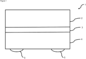
- the bond pad comprises a copper foil 2 having a plating layer 3 on its surface.
- a sinterable silver film 4 is laminated on the copper foil 2 via the plating later 3.
- Tack agent 5 is situated on the outer surface of the sinterable silver film 4.
- FIG. 2 there is shown an electronic device (generally at 6) according to the present invention.
- a bond pad 1 according to the present invention is attached to a die 7 via the sinterable silver film of the bond pad (not shown).
- the die 7 is attached via a sinterable silver film 8 to a substrate 9.
- the substrate comprises a ceramic core 10 and a copper surface layer 11.
- a copper wire 12 is welded to the top of the bond pad 1 and the copper surface layer 11.
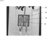
- An electronic device was prepared according to the following method.
- a substrate was provided having a die thereon, the substrate and die separated by a sinterable film.
- a 50 ⁇ m thick bond pad was prepared comprising a metal plated hard copper foil having sinterable silver film laminated thereon.
- the bond pad was placed via the sinterable film onto the top of the die.
- the resulting blank was transferred to an oven where the sinterable films were sintered to form metallic joints between the bond pad and the top of the die, and between the die and the substrate. Copper ribbons were then ultrasonically welded to the top of the bod pad.
- the results are shown in Figure 3 with the bond pad labelled 13, the die labelled 14, the substrate labelled 15 and the copper ribbons labelled 16.
Landscapes
- Engineering & Computer Science (AREA)
- Manufacturing & Machinery (AREA)
- Chemical & Material Sciences (AREA)
- Composite Materials (AREA)
- Materials Engineering (AREA)
- Mechanical Engineering (AREA)
- Laminated Bodies (AREA)
- Powder Metallurgy (AREA)
- Manufacturing Of Printed Wiring (AREA)
- Production Of Multi-Layered Print Wiring Board (AREA)
- Die Bonding (AREA)
Applications Claiming Priority (3)
| Application Number | Priority Date | Filing Date | Title |
|---|---|---|---|
| US202263319891P | 2022-03-15 | 2022-03-15 | |
| EP23713579.3A EP4494182B1 (de) | 2022-03-15 | 2023-03-15 | Sinterbereite mehrschichtige draht-/bandbondpads und verfahren zur chipoberbefestigung |
| PCT/EP2023/025116 WO2023174581A1 (en) | 2022-03-15 | 2023-03-15 | Sinter ready multilayer wire/ribbon bond pads and method for die top attachment |
Related Parent Applications (2)
| Application Number | Title | Priority Date | Filing Date |
|---|---|---|---|
| EP23713579.3A Division EP4494182B1 (de) | 2022-03-15 | 2023-03-15 | Sinterbereite mehrschichtige draht-/bandbondpads und verfahren zur chipoberbefestigung |
| EP23713579.3A Division-Into EP4494182B1 (de) | 2022-03-15 | 2023-03-15 | Sinterbereite mehrschichtige draht-/bandbondpads und verfahren zur chipoberbefestigung |
Publications (2)
| Publication Number | Publication Date |
|---|---|
| EP4550399A2 true EP4550399A2 (de) | 2025-05-07 |
| EP4550399A3 EP4550399A3 (de) | 2025-07-30 |
Family
ID=85775944
Family Applications (2)
| Application Number | Title | Priority Date | Filing Date |
|---|---|---|---|
| EP25156858.0A Pending EP4550399A3 (de) | 2022-03-15 | 2023-03-15 | Sinterbereite multilaterdraht/band-bondpads und verfahren zur chipoberbefestigung |
| EP23713579.3A Active EP4494182B1 (de) | 2022-03-15 | 2023-03-15 | Sinterbereite mehrschichtige draht-/bandbondpads und verfahren zur chipoberbefestigung |
Family Applications After (1)
| Application Number | Title | Priority Date | Filing Date |
|---|---|---|---|
| EP23713579.3A Active EP4494182B1 (de) | 2022-03-15 | 2023-03-15 | Sinterbereite mehrschichtige draht-/bandbondpads und verfahren zur chipoberbefestigung |
Country Status (8)
| Country | Link |
|---|---|
| US (1) | US20250201741A1 (de) |
| EP (2) | EP4550399A3 (de) |
| JP (1) | JP2025508013A (de) |
| KR (1) | KR20240161145A (de) |
| CN (1) | CN118786521A (de) |
| DK (1) | DK4494182T3 (de) |
| TW (1) | TW202345248A (de) |
| WO (1) | WO2023174581A1 (de) |
Families Citing this family (1)
| Publication number | Priority date | Publication date | Assignee | Title |
|---|---|---|---|---|
| EP4700826A1 (de) * | 2024-08-23 | 2026-02-25 | Heraeus Electronics GmbH & Co. KG | Substratanordnung, verfahren zur herstellung einer elektronischen baugruppe und elektronische baugruppe |
Citations (3)
| Publication number | Priority date | Publication date | Assignee | Title |
|---|---|---|---|---|
| US10079219B2 (en) | 2014-11-07 | 2018-09-18 | Danfoss Silicon Power Gmbh | Power semiconductor contact structure and method for the production thereof |
| US10535628B2 (en) | 2010-11-03 | 2020-01-14 | Alpha Assembly Solutions Inc. | Sintering materials and attachment methods using same |
| US10710336B2 (en) | 2013-08-29 | 2020-07-14 | Alpha Assembly Solutions Inc. | Composite and multilayered silver films for joining electrical and mechanical components |
Family Cites Families (8)
| Publication number | Priority date | Publication date | Assignee | Title |
|---|---|---|---|---|
| TW201611198A (zh) * | 2014-04-11 | 2016-03-16 | 阿爾發金屬公司 | 低壓燒結粉末 |
| WO2015192004A1 (en) * | 2014-06-12 | 2015-12-17 | Alpha Metals, Inc. | Sintering materials and attachment methods using same |
| DE102014109766B3 (de) * | 2014-07-11 | 2015-04-02 | Heraeus Deutschland GmbH & Co. KG | Verfahren zum Herstellen eines Substratadapters, Substratadapter und Verfahren zum Kontaktieren eines Halbleiterelements |
| DE102014117246B4 (de) * | 2014-11-25 | 2018-11-15 | Heraeus Deutschland GmbH & Co. KG | Verfahren zum Herstellen eines Substratadapters, Substratadapter und Verfahren zum Kontaktieren eines Halbleiterelements |
| JP6466594B2 (ja) * | 2014-12-17 | 2019-02-06 | アルファ・アセンブリー・ソリューションズ・インコーポレイテッドAlpha Assembly Solutions Inc. | ダイとクリップの接着方法 |
| CN109643661B (zh) * | 2016-08-05 | 2022-09-09 | 三菱电机株式会社 | 功率半导体装置 |
| JP7124049B2 (ja) * | 2018-02-22 | 2022-08-23 | リンテック株式会社 | フィルム状焼成材料、及び支持シート付フィルム状焼成材料 |
| JP7198693B2 (ja) * | 2019-03-15 | 2023-01-04 | 日東電工株式会社 | 焼結接合用シートおよび基材付き焼結接合用シート |
-
2023
- 2023-03-15 DK DK23713579.3T patent/DK4494182T3/da active
- 2023-03-15 EP EP25156858.0A patent/EP4550399A3/de active Pending
- 2023-03-15 KR KR1020247033332A patent/KR20240161145A/ko active Pending
- 2023-03-15 EP EP23713579.3A patent/EP4494182B1/de active Active
- 2023-03-15 TW TW112109617A patent/TW202345248A/zh unknown
- 2023-03-15 CN CN202380026794.6A patent/CN118786521A/zh active Pending
- 2023-03-15 US US18/845,736 patent/US20250201741A1/en active Pending
- 2023-03-15 WO PCT/EP2023/025116 patent/WO2023174581A1/en not_active Ceased
- 2023-03-15 JP JP2024552782A patent/JP2025508013A/ja active Pending
Patent Citations (3)
| Publication number | Priority date | Publication date | Assignee | Title |
|---|---|---|---|---|
| US10535628B2 (en) | 2010-11-03 | 2020-01-14 | Alpha Assembly Solutions Inc. | Sintering materials and attachment methods using same |
| US10710336B2 (en) | 2013-08-29 | 2020-07-14 | Alpha Assembly Solutions Inc. | Composite and multilayered silver films for joining electrical and mechanical components |
| US10079219B2 (en) | 2014-11-07 | 2018-09-18 | Danfoss Silicon Power Gmbh | Power semiconductor contact structure and method for the production thereof |
Also Published As
| Publication number | Publication date |
|---|---|
| KR20240161145A (ko) | 2024-11-12 |
| EP4494182A1 (de) | 2025-01-22 |
| EP4550399A3 (de) | 2025-07-30 |
| DK4494182T3 (da) | 2026-03-16 |
| EP4494182B1 (de) | 2026-02-18 |
| CN118786521A (zh) | 2024-10-15 |
| TW202345248A (zh) | 2023-11-16 |
| US20250201741A1 (en) | 2025-06-19 |
| JP2025508013A (ja) | 2025-03-21 |
| WO2023174581A1 (en) | 2023-09-21 |
Similar Documents
| Publication | Publication Date | Title |
|---|---|---|
| US20260018559A1 (en) | Sintering materials and attachment methods using same | |
| US11389865B2 (en) | Sintering materials and attachment methods using same | |
| EP2617515B1 (de) | Klebematerial für halbleiterbauelemente | |
| CN105473257B (zh) | 金属烧结膜组合物 | |
| EP3048640B1 (de) | Verfahren zur herstellung eines trägersubstrats mit einem elektronischen teil | |
| EP4494182B1 (de) | Sinterbereite mehrschichtige draht-/bandbondpads und verfahren zur chipoberbefestigung | |
| HK40111025A (zh) | 烧结就绪多层线/带键合焊盘和用於管芯顶部附接的方法 | |
| WO2023138902A2 (en) | Method of joining electrical and mechanical components using laminated modular preforms | |
| JP2006120973A (ja) | 回路基板および回路基板の製造方法 | |
| JP4095468B2 (ja) | ガラスセラミック基板の製造方法 | |
| US20260123502A1 (en) | Method of joining electrical and mechanical components using laminated modular preforms | |
| JPS6334963A (ja) | 半導体装置用セラミツク基板の製造方法およびその方法に使用するクラツド材 | |
| JP2025082602A (ja) | ニッケル系金属板一体型セラミックス基板およびその製造方法 | |
| WO2016143631A1 (ja) | 接合体の製造方法、ヒートシンク付パワーモジュール用基板の製造方法、及び、ヒートシンクの製造方法 |
Legal Events
| Date | Code | Title | Description |
|---|---|---|---|
| PUAI | Public reference made under article 153(3) epc to a published international application that has entered the european phase |
Free format text: ORIGINAL CODE: 0009012 |
|
| STAA | Information on the status of an ep patent application or granted ep patent |
Free format text: STATUS: REQUEST FOR EXAMINATION WAS MADE |
|
| 17P | Request for examination filed |
Effective date: 20250210 |
|
| AC | Divisional application: reference to earlier application |
Ref document number: 4494182 Country of ref document: EP Kind code of ref document: P |
|
| AK | Designated contracting states |
Kind code of ref document: A2 Designated state(s): AL AT BE BG CH CY CZ DE DK EE ES FI FR GB GR HR HU IE IS IT LI LT LU LV MC ME MK MT NL NO PL PT RO RS SE SI SK SM TR |
|
| PUAL | Search report despatched |
Free format text: ORIGINAL CODE: 0009013 |
|
| AK | Designated contracting states |
Kind code of ref document: A3 Designated state(s): AL AT BE BG CH CY CZ DE DK EE ES FI FR GB GR HR HU IE IS IT LI LT LU LV MC ME MK MT NL NO PL PT RO RS SE SI SK SM TR |
|
| RIC1 | Information provided on ipc code assigned before grant |
Ipc: H01L 23/00 20060101AFI20250624BHEP |