EP4550364A1 - Method for manufacturing superconducting wire material - Google Patents
Method for manufacturing superconducting wire material Download PDFInfo
- Publication number
- EP4550364A1 EP4550364A1 EP24825651.3A EP24825651A EP4550364A1 EP 4550364 A1 EP4550364 A1 EP 4550364A1 EP 24825651 A EP24825651 A EP 24825651A EP 4550364 A1 EP4550364 A1 EP 4550364A1
- Authority
- EP
- European Patent Office
- Prior art keywords
- substrate
- layer
- main surface
- ion beam
- superconducting wire
- Prior art date
- Legal status (The legal status is an assumption and is not a legal conclusion. Google has not performed a legal analysis and makes no representation as to the accuracy of the status listed.)
- Pending
Links
Images



Classifications
-
- H—ELECTRICITY
- H10—SEMICONDUCTOR DEVICES; ELECTRIC SOLID-STATE DEVICES NOT OTHERWISE PROVIDED FOR
- H10N—ELECTRIC SOLID-STATE DEVICES NOT OTHERWISE PROVIDED FOR
- H10N60/00—Superconducting devices
- H10N60/01—Manufacture or treatment
- H10N60/0268—Manufacture or treatment of devices comprising copper oxide
- H10N60/0296—Processes for depositing or forming copper oxide superconductor layers
- H10N60/0576—Processes for depositing or forming copper oxide superconductor layers characterised by the substrate
- H10N60/0632—Intermediate layers, e.g. for growth control
-
- C—CHEMISTRY; METALLURGY
- C23—COATING METALLIC MATERIAL; COATING MATERIAL WITH METALLIC MATERIAL; CHEMICAL SURFACE TREATMENT; DIFFUSION TREATMENT OF METALLIC MATERIAL; COATING BY VACUUM EVAPORATION, BY SPUTTERING, BY ION IMPLANTATION OR BY CHEMICAL VAPOUR DEPOSITION, IN GENERAL; INHIBITING CORROSION OF METALLIC MATERIAL OR INCRUSTATION IN GENERAL
- C23C—COATING METALLIC MATERIAL; COATING MATERIAL WITH METALLIC MATERIAL; SURFACE TREATMENT OF METALLIC MATERIAL BY DIFFUSION INTO THE SURFACE, BY CHEMICAL CONVERSION OR SUBSTITUTION; COATING BY VACUUM EVAPORATION, BY SPUTTERING, BY ION IMPLANTATION OR BY CHEMICAL VAPOUR DEPOSITION, IN GENERAL
- C23C14/00—Coating by vacuum evaporation, by sputtering or by ion implantation of the coating forming material
- C23C14/0021—Reactive sputtering or evaporation
- C23C14/0026—Activation or excitation of reactive gases outside the coating chamber
- C23C14/0031—Bombardment of substrates by reactive ion beams
-
- C—CHEMISTRY; METALLURGY
- C23—COATING METALLIC MATERIAL; COATING MATERIAL WITH METALLIC MATERIAL; CHEMICAL SURFACE TREATMENT; DIFFUSION TREATMENT OF METALLIC MATERIAL; COATING BY VACUUM EVAPORATION, BY SPUTTERING, BY ION IMPLANTATION OR BY CHEMICAL VAPOUR DEPOSITION, IN GENERAL; INHIBITING CORROSION OF METALLIC MATERIAL OR INCRUSTATION IN GENERAL
- C23C—COATING METALLIC MATERIAL; COATING MATERIAL WITH METALLIC MATERIAL; SURFACE TREATMENT OF METALLIC MATERIAL BY DIFFUSION INTO THE SURFACE, BY CHEMICAL CONVERSION OR SUBSTITUTION; COATING BY VACUUM EVAPORATION, BY SPUTTERING, BY ION IMPLANTATION OR BY CHEMICAL VAPOUR DEPOSITION, IN GENERAL
- C23C14/00—Coating by vacuum evaporation, by sputtering or by ion implantation of the coating forming material
- C23C14/06—Coating by vacuum evaporation, by sputtering or by ion implantation of the coating forming material characterised by the coating material
- C23C14/08—Oxides
- C23C14/081—Oxides of aluminium, magnesium or beryllium
-
- C—CHEMISTRY; METALLURGY
- C23—COATING METALLIC MATERIAL; COATING MATERIAL WITH METALLIC MATERIAL; CHEMICAL SURFACE TREATMENT; DIFFUSION TREATMENT OF METALLIC MATERIAL; COATING BY VACUUM EVAPORATION, BY SPUTTERING, BY ION IMPLANTATION OR BY CHEMICAL VAPOUR DEPOSITION, IN GENERAL; INHIBITING CORROSION OF METALLIC MATERIAL OR INCRUSTATION IN GENERAL
- C23C—COATING METALLIC MATERIAL; COATING MATERIAL WITH METALLIC MATERIAL; SURFACE TREATMENT OF METALLIC MATERIAL BY DIFFUSION INTO THE SURFACE, BY CHEMICAL CONVERSION OR SUBSTITUTION; COATING BY VACUUM EVAPORATION, BY SPUTTERING, BY ION IMPLANTATION OR BY CHEMICAL VAPOUR DEPOSITION, IN GENERAL
- C23C14/00—Coating by vacuum evaporation, by sputtering or by ion implantation of the coating forming material
- C23C14/22—Coating by vacuum evaporation, by sputtering or by ion implantation of the coating forming material characterised by the process of coating
- C23C14/24—Vacuum evaporation
- C23C14/28—Vacuum evaporation by wave energy or particle radiation
- C23C14/30—Vacuum evaporation by wave energy or particle radiation by electron bombardment
-
- C—CHEMISTRY; METALLURGY
- C23—COATING METALLIC MATERIAL; COATING MATERIAL WITH METALLIC MATERIAL; CHEMICAL SURFACE TREATMENT; DIFFUSION TREATMENT OF METALLIC MATERIAL; COATING BY VACUUM EVAPORATION, BY SPUTTERING, BY ION IMPLANTATION OR BY CHEMICAL VAPOUR DEPOSITION, IN GENERAL; INHIBITING CORROSION OF METALLIC MATERIAL OR INCRUSTATION IN GENERAL
- C23C—COATING METALLIC MATERIAL; COATING MATERIAL WITH METALLIC MATERIAL; SURFACE TREATMENT OF METALLIC MATERIAL BY DIFFUSION INTO THE SURFACE, BY CHEMICAL CONVERSION OR SUBSTITUTION; COATING BY VACUUM EVAPORATION, BY SPUTTERING, BY ION IMPLANTATION OR BY CHEMICAL VAPOUR DEPOSITION, IN GENERAL
- C23C14/00—Coating by vacuum evaporation, by sputtering or by ion implantation of the coating forming material
- C23C14/58—After-treatment
- C23C14/5826—Treatment with charged particles
- C23C14/5833—Ion beam bombardment
-
- H—ELECTRICITY
- H01—ELECTRIC ELEMENTS
- H01B—CABLES; CONDUCTORS; INSULATORS; SELECTION OF MATERIALS FOR THEIR CONDUCTIVE, INSULATING OR DIELECTRIC PROPERTIES
- H01B12/00—Superconductive or hyperconductive conductors, cables, or transmission lines
- H01B12/02—Superconductive or hyperconductive conductors, cables, or transmission lines characterised by their form
- H01B12/06—Films or wires on bases or cores
Definitions
- the present disclosure relates to a method for manufacturing a superconducting wire.
- the present application claims priority to Japanese Patent Application No. 2023-102493 filed on June 22, 2023 .
- the entire content of the Japanese patent application is herein incorporated by reference.
- Japanese Patent Laying-Open No. 2012-64519 discloses a superconducting wire.
- the superconducting wire disclosed in PTL 1 includes a metal substrate and an buffer layer.
- the metal substrate includes a main surface.
- the buffer layer is disposed on the main surface of the metal substrate.
- a method for manufacturing a superconducting wire according to the present disclosure is a method for manufacturing a superconducting wire including a substrate having a main surface, and an buffer layer disposed on the main surface.
- the method for manufacturing a superconducting wire includes forming the buffer layer on the main surface.
- the substrate has a width of 15 mm or more in a width direction of the substrate orthogonal to a longitudinal direction of the substrate.
- the buffer layer includes an IBAD (Ion Beam Assisted Deposition) layer.
- the IBAD layer is formed by supplying, onto the main surface, a constituent material, being in an evaporated form, of the IBAD layer, while applying an ion beam from an ion beam source onto the main surface, in a state in which the substrate is transported in the longitudinal direction of the substrate.
- a direction in which the ion beam is applied is inclined with respect to a direction normal to the main surface.
- a longitudinal direction of the ion beam source is along the width direction of the substrate.
- the buffer layer is formed by an ion beam assisted deposition (IBAD) method. More specifically, an ion beam is applied onto the main surface of the metal substrate, while supplying a constituent material, in an evaporated form, of the buffer layer onto the main surface of the metal substrate, in a state in which the metal substrate is transported in the longitudinal direction of the metal substrate, to thereby form the buffer layer.
- IBAD ion beam assisted deposition
- the direction in which the ion beam is applied is inclined with respect to the main surface of the metal substrate.
- the longitudinal direction of an assisted ion source applying the ion beam is along the longitudinal direction of the metal substrate. Therefore, when the superconducting wire disclosed in PTL 1 has a large width, the angle at which the ion beam is applied with respect to the main surface varies depending on the position in the width direction. Consequently, the uniformness in the quality of the buffer layer is impaired.
- the present disclosure is made in view of the problem with the conventional technique as set forth above. More specifically, the present disclosure provides a method for manufacturing a superconducting wire improved in uniformity of the quality of the IBAD layer formed by the IBAD method.
- the method for manufacturing a superconducting wire described above in (1) enables improvement in uniformity of the quality of the IBAD layer.
- the substrate may be transported to pass, once or multiple times, in a direction in which the substrate is transported, across a region to which the ion beam is applied.
- the method for manufacturing a superconducting wire described above in (2) enables improvement in productivity of the superconducting wire, by eliminating the need to move the substrate multiple times around transport mechanisms such as rolls.
- the constituent material, being in the evaporated form, of the IBAD layer may be generated by being evaporated by irradiation with an electron beam, and then supplied onto the main surface.
- the method for manufacturing a superconducting wire described above in (3) enables improvement in productivity of the superconducting wire, by improvement in the deposition rate of the IBAD layer (by shortening of the time taken to deposit the layer).
- the constituent material of the IBAD layer may be magnesium oxide.
- a constituent material of the substrate may be Hastelloy (registered trademark) or stainless steel.
- a configuration of a superconducting wire 10 is described in the following.
- superconducting wire 10 includes a substrate 11, an buffer layer 12, and a superconducting layer 13.
- Substrate 11 includes a main surface 11a and a main surface 11b.
- Main surface 11a and main surface 11b are end faces in the thickness direction of substrate 11.
- Main surface 11b is a surface opposite to main surface 11a.
- a constituent material of substrate 11 is, for example, a metal material such as Hastelloy or stainless steel. However, the constituent material of substrate 11 is not limited thereto.
- Buffer layer 12 is disposed on substrate 11. Buffer layer 12 is disposed on main surface 11a. Buffer layer 12 includes an underlayer 12a, an IBAD layer 12b, and a surface layer 12c.
- Underlayer 12a is disposed on main surface 11a.
- Underlayer 12a is a layer that prevents diffusion of oxygen and diffusion of constituent elements of substrate 11.
- Underlayer 12a may be made up of a plurality of layers.
- Underlayer 12a may be made up of, for example, an amorphous aluminum oxide (Al 2 O 3 ) layer disposed on main surface 11a and an amorphous yttrium oxide (Y 2 O 3 ) layer disposed on the aluminum oxide layer.
- Al 2 O 3 amorphous aluminum oxide
- Y 2 O 3 amorphous yttrium oxide
- the layer configuration of underlayer 12a is not limited thereto.
- IBAD layer 12b is a layer formed by the IBAD method. That is, in IBAD layer 12b, crystals of the constituent material are oriented. IBAD layer 12b is disposed on underlayer 12a.
- a constituent material of IBAD layer 12b is, for example, magnesium oxide (MgO). However, the constituent material of IBAD layer 12b is not limited thereto.
- Superconducting layer 13 is disposed on buffer layer 12 (surface layer 12c).
- a constituent material of superconducting layer 13 is an oxide superconductor.
- the oxide superconductor include REBa 2 Cu 3 O x .
- RE is a rare earth element.
- the rare earth element include gadolinium (Gd), yttrium (Y), europium (Eu), holmium (Ho), ytterbium (Yb), samarium (Sm), dysprosium (Dy), and neodymium (Nd).
- the rare earth element is not limited thereto.
- the crystals of the constituent material are oriented in surface layer 12c, and therefore, in superconducting layer 13 as well, crystals of its constituent material are also oriented. More specifically, in superconducting layer 13, the c-axis of the crystals of the constituent material is oriented in the direction normal to main surface 11a.
- Width W is the width of substrate 11 in the width direction orthogonal to the longitudinal direction of substrate 11.
- Width W is, for example, 15 mm or more.
- Width W may be 20 mm or more, 30 mm or more, 50 mm or more, or 100 mm or more.
- Width W may be, for example, 300 mm or less, 250 mm or less, or 200 mm or less.
- Width W may be 15 mm or more and 300 mm or less, 15 mm or more and 250 mm or less, or 15 mm or more and 200 mm or less.
- Width W may be 20 mm or more and 300 mm or less, 20 mm or more and 250 mm or less, or 20 mm or more and 200 mm or less. Width W may be 30 mm or more and 300 mm or less, 30 mm or more and 250 mm or less, or 30 mm or more and 200 mm or less. Width W may be 50 mm or more and 300 mm or less, 50 mm or more and 250 mm or less, or 50 mm or more and 200 mm or less. Width W may be 100 mm or more and 300 mm or less, 100 mm or more and 250 mm or less, or 100 mm or more and 200 mm or less.
- a method for manufacturing superconducting wire 10 is described in the following.
- the method for manufacturing superconducting wire 10 includes a preparation step S1, an underlayer formation step S2, an IBAD step S3, a surface layer formation step S4, and a superconducting layer formation step S5.
- Evaporation mechanism 30 includes a filament 31 and a coil 32. Application of a voltage to filament 31 causes electrons to be emitted from filament 31. The electrons emitted from filament 31 are accelerated by a potential difference between filament 31 and crucible 20, and the electrons with their trajectory bent by coil 32 form an electron beam EB. Application of electron beam EB to raw material M causes raw material M to be evaporated into evaporated raw material MG.
- Evaporated raw material MG is supplied while being irradiated with ion beam IB, so that IBAD layer 12b in which crystals of its constituent material are oriented is grown on main surface 11a (underlayer 12a).
- IBAD step S3 surface layer formation step S4 is performed.
- surface layer 12c is formed on IBAD layer 12b by, for example, magnetron sputtering.
- superconducting layer formation step S5 is performed.
- superconducting layer 13 is formed on buffer layer 12 by, for example, MOD (Metal Organic Decomposition) method, PLD (Pulsed Laser Deposition) method, MOCVD (Metal Organic Chemical Vapor Deposition) method, or the like. In this way, the structure of superconducting wire 10 shown in Figs. 1 and 2 is formed.
- superconducting wire 10 may be slit (cut) into a plurality of superconducting wires in the longitudinal direction of substrate 11.
- a stabilizing layer which is not shown, may be formed on superconducting layer 13.
- a protective layer may be formed on the stabilizing layer.
- the constituent material of the stabilizing layer and the constituent material of the protective layer are, for example, silver (Ag) and copper (Cu), respectively.
- substrate 11 having a large width W of 15 mm or more is used.
- IBAD layer 12b is formed using substrate 11 having such a large width and the longitudinal direction of ion beam source 40 is along the longitudinal direction of substrate 11, the incident angle of ion beam IB varies depending on the position in the width direction of substrate 11. As a result, the quality of IBAD layer 12b also changes depending on the position in the width direction of substrate 11, and it is difficult to obtain uniform quality of IBAD layer 12b.
- the method for manufacturing superconducting wire 10 does not require the step of moving substrate 11 multiple times around transport mechanisms such as rolls, and can form IBAD layer 12b with a large width at a time, so that the productivity of superconducting wire 10 is improved.
- the smaller the distance DIS the larger the dimension of the region of ion beam IB in which the intensity falls within a predetermined range, in the longitudinal direction of ion beam source 40. That is, the smaller the distance DIS, the easier the uniformity of the film quality of IBAD layer 12b is ensured. Meanwhile, if distance DIS is too small, the temperature of substrate 11 becomes too high, and the crystals of the constituent material are difficult to be oriented in IBAD layer 12b.
- distance DIS When distance DIS is about 40 cm, it is possible to ensure that the dimension of the region of ion beam IB in which the intensity is within a predetermined range, in the longitudinal direction of ion beam source 40, is about 100 mm. Therefore, in the method for manufacturing superconducting wire 10, distance DIS is set to 10 cm or more and 40 cm or less to thereby enable improvement of the uniformity of the quality of IBAD layer 12b while suppressing deterioration in the degree of orientation of the crystals of the constituent material in IBAD layer 12b.
Landscapes
- Chemical & Material Sciences (AREA)
- Engineering & Computer Science (AREA)
- Chemical Kinetics & Catalysis (AREA)
- Materials Engineering (AREA)
- Mechanical Engineering (AREA)
- Metallurgy (AREA)
- Organic Chemistry (AREA)
- Health & Medical Sciences (AREA)
- Toxicology (AREA)
- Manufacturing & Machinery (AREA)
- Superconductors And Manufacturing Methods Therefor (AREA)
Abstract
Description
- The present disclosure relates to a method for manufacturing a superconducting wire. The present application claims priority to
Japanese Patent Application No. 2023-102493 filed on June 22, 2023 - For example,
Japanese Patent Laying-Open No. 2012-64519
The buffer layer is disposed on the main surface of the metal substrate. - PTL 1:
Japanese Patent Laying-Open No. 2012-64519 - A method for manufacturing a superconducting wire according to the present disclosure is a method for manufacturing a superconducting wire including a substrate having a main surface, and an buffer layer disposed on the main surface. The method for manufacturing a superconducting wire includes forming the buffer layer on the main surface. The substrate has a width of 15 mm or more in a width direction of the substrate orthogonal to a longitudinal direction of the substrate. The buffer layer includes an IBAD (Ion Beam Assisted Deposition) layer. The IBAD layer is formed by supplying, onto the main surface, a constituent material, being in an evaporated form, of the IBAD layer, while applying an ion beam from an ion beam source onto the main surface, in a state in which the substrate is transported in the longitudinal direction of the substrate. A direction in which the ion beam is applied is inclined with respect to a direction normal to the main surface. A longitudinal direction of the ion beam source is along the width direction of the substrate.
-
-
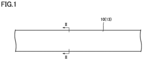
Fig. 1 is a plan view of asuperconducting wire 10. -
Fig. 2 is a cross-sectional view taken along II-II inFig. 1 . -
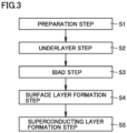
Fig. 3 is a flowchart of steps for manufacturingsuperconducting wire 10. -
Fig. 4 is a schematic side view illustrating IBAD step S3. -
Fig. 5 is a schematic front view illustrating IBAD step S3. -
Fig. 6 is a schematic perspective view illustrating a relation between asubstrate 11 and anion beam source 40. - In the superconducting wire disclosed in PTL 1, the buffer layer is formed by an ion beam assisted deposition (IBAD) method. More specifically, an ion beam is applied onto the main surface of the metal substrate, while supplying a constituent material, in an evaporated form, of the buffer layer onto the main surface of the metal substrate, in a state in which the metal substrate is transported in the longitudinal direction of the metal substrate, to thereby form the buffer layer.
- In this case, the direction in which the ion beam is applied is inclined with respect to the main surface of the metal substrate. Moreover, the longitudinal direction of an assisted ion source applying the ion beam is along the longitudinal direction of the metal substrate. Therefore, when the superconducting wire disclosed in PTL 1 has a large width, the angle at which the ion beam is applied with respect to the main surface varies depending on the position in the width direction. Consequently, the uniformness in the quality of the buffer layer is impaired.
- The present disclosure is made in view of the problem with the conventional technique as set forth above. More specifically, the present disclosure provides a method for manufacturing a superconducting wire improved in uniformity of the quality of the IBAD layer formed by the IBAD method.
- With the method for manufacturing a superconducting wire according to the present disclosure, the uniformity of the quality of the IBAD layer can be improved.
- Initially, embodiments of the present disclosure are described one by one.
- (1) A method for manufacturing a superconducting wire according to an embodiment is a method for manufacturing a superconducting wire including a substrate having a main surface, and an buffer layer disposed on the main surface. The method for manufacturing a superconducting wire includes forming the buffer layer on the main surface. The substrate has a width of 15 mm or more in a width direction of the substrate orthogonal to a longitudinal direction of the substrate. The buffer layer includes an IBAD layer. The IBAD layer is formed by supplying, onto the main surface, a constituent material, being in an evaporated form, of the IBAD layer, while applying an ion beam from an ion beam source onto the main surface, in a state in which the substrate is transported in the longitudinal direction of the substrate. A direction in which the ion beam is applied is inclined with respect to a direction normal to the main surface. A longitudinal direction of the ion beam source is along the width direction of the substrate.
- The method for manufacturing a superconducting wire described above in (1) enables improvement in uniformity of the quality of the IBAD layer.
- (2) In the method for manufacturing a superconducting wire described above in (1), the substrate may be transported to pass, once or multiple times, in a direction in which the substrate is transported, across a region to which the ion beam is applied.
- The method for manufacturing a superconducting wire described above in (2) enables improvement in productivity of the superconducting wire, by eliminating the need to move the substrate multiple times around transport mechanisms such as rolls.
- (3) In the method for manufacturing a superconducting wire described above in (1) or (2), the constituent material, being in the evaporated form, of the IBAD layer may be generated by being evaporated by irradiation with an electron beam, and then supplied onto the main surface.
- The method for manufacturing a superconducting wire described above in (3) enables improvement in productivity of the superconducting wire, by improvement in the deposition rate of the IBAD layer (by shortening of the time taken to deposit the layer).
- (4) In the method for manufacturing a superconducting wire described above in (1) to (3), the constituent material of the IBAD layer may be magnesium oxide.
- (5) In the method for manufacturing a superconducting wire described above in (1) to (4), a constituent material of the substrate may be Hastelloy (registered trademark) or stainless steel.
- Next, details of embodiments of the present disclosure are described with reference to the drawings. In the following drawings, the same or corresponding parts are denoted by the same reference characters, and a description thereof is not herein repeated.
- A configuration of a
superconducting wire 10 is described in the following. - As shown in
Figs. 1 and2 ,superconducting wire 10 includes asubstrate 11, anbuffer layer 12, and asuperconducting layer 13. -
Substrate 11 includes amain surface 11a and a main surface 11b.Main surface 11a and main surface 11b are end faces in the thickness direction ofsubstrate 11. Main surface 11b is a surface opposite tomain surface 11a. A constituent material ofsubstrate 11 is, for example, a metal material such as Hastelloy or stainless steel. However, the constituent material ofsubstrate 11 is not limited thereto. -
Buffer layer 12 is disposed onsubstrate 11.Buffer layer 12 is disposed onmain surface 11a.Buffer layer 12 includes an underlayer 12a, an IBAD layer 12b, and asurface layer 12c. - Underlayer 12a is disposed on
main surface 11a. Underlayer 12a is a layer that prevents diffusion of oxygen and diffusion of constituent elements ofsubstrate 11. Underlayer 12a may be made up of a plurality of layers. Underlayer 12a may be made up of, for example, an amorphous aluminum oxide (Al2O3) layer disposed onmain surface 11a and an amorphous yttrium oxide (Y2O3) layer disposed on the aluminum oxide layer. However, the layer configuration of underlayer 12a is not limited thereto. - IBAD layer 12b is a layer formed by the IBAD method. That is, in IBAD layer 12b, crystals of the constituent material are oriented. IBAD layer 12b is disposed on underlayer 12a. A constituent material of IBAD layer 12b is, for example, magnesium oxide (MgO). However, the constituent material of IBAD layer 12b is not limited thereto.
-
Surface layer 12c is disposed on IBAD layer 12b. As described above, the crystals of the constituent material are oriented in IBAD layer 12b, and therefore, insurface layer 12c as well, crystals of its constituent material are also oriented.Surface layer 12c is made up of a plurality of layers.Surface layer 12c is made up of, for example, a magnesium oxide layer disposed on IBAD layer 12b and a lanthanum manganite (LaMnO3) layer disposed on the magnesium oxide layer.Surface layer 12c may be a single layer. In this case, a constituent material ofsurface layer 12c is, for example, cerium oxide (CeO2). However, the layer configuration ofsurface layer 12c is not limited thereto. -
Superconducting layer 13 is disposed on buffer layer 12 (surface layer 12c). A constituent material ofsuperconducting layer 13 is an oxide superconductor. Specific examples of the oxide superconductor include REBa2Cu3Ox. Here, RE is a rare earth element. Examples of the rare earth element include gadolinium (Gd), yttrium (Y), europium (Eu), holmium (Ho), ytterbium (Yb), samarium (Sm), dysprosium (Dy), and neodymium (Nd). However, the rare earth element is not limited thereto. As described above, the crystals of the constituent material are oriented insurface layer 12c, and therefore, insuperconducting layer 13 as well, crystals of its constituent material are also oriented. More specifically, insuperconducting layer 13, the c-axis of the crystals of the constituent material is oriented in the direction normal tomain surface 11a. - The width of
substrate 11 is defined as width W. Width W is the width ofsubstrate 11 in the width direction orthogonal to the longitudinal direction ofsubstrate 11. Width W is, for example, 15 mm or more. Width W may be 20 mm or more, 30 mm or more, 50 mm or more, or 100 mm or more. Width W may be, for example, 300 mm or less, 250 mm or less, or 200 mm or less. Width W may be 15 mm or more and 300 mm or less, 15 mm or more and 250 mm or less, or 15 mm or more and 200 mm or less. Width W may be 20 mm or more and 300 mm or less, 20 mm or more and 250 mm or less, or 20 mm or more and 200 mm or less. Width W may be 30 mm or more and 300 mm or less, 30 mm or more and 250 mm or less, or 30 mm or more and 200 mm or less. Width W may be 50 mm or more and 300 mm or less, 50 mm or more and 250 mm or less, or 50 mm or more and 200 mm or less. Width W may be 100 mm or more and 300 mm or less, 100 mm or more and 250 mm or less, or 100 mm or more and 200 mm or less. - A method for manufacturing
superconducting wire 10 is described in the following. - As shown in
Fig. 3 , the method for manufacturingsuperconducting wire 10 includes a preparation step S1, an underlayer formation step S2, an IBAD step S3, a surface layer formation step S4, and a superconducting layer formation step S5. - In preparation step S1,
substrate 11 is prepared. After preparation step S1, underlayer formation step S2 is performed. In underlayer formation step S2, underlayer 12a is formed onmain surface 11a by, for example, magnetron sputtering. After underlayer formation step S2, IBAD step S3 is performed. - As shown in
Figs. 4 to 6 , IBAD step S3 is performed using afilm deposition apparatus 100.Film deposition apparatus 100 includes acrucible 20, a rawmaterial supply mechanism 21, anevaporation mechanism 30, anion beam source 40, ashield plate 50, and aheat equalization plate 60.Film deposition apparatus 100 further includes a transport mechanism, which is not shown. - In IBAD step S3,
substrate 11 is transported in the longitudinal direction ofsubstrate 11 by the transport mechanism (see black arrows inFig. 4 andFig. 6 ).Substrate 11 is transported overshield plate 50.Main surface 11a (underlayer 12a) facesshield plate 50 with a space therebetween. Anopening 51 extending throughshield plate 50 in the thickness direction is formed inshield plate 50. For example,substrate 11 is transported so as to pass across a region irradiated with an ion beam IB (described later herein) without turning back, namely, so as to pass across the region irradiated with ion beam IB, only once in the transport direction in which it is transported. That is,substrate 11 is transported in a single-turn manner instead of a multi-turn manner (seeFig. 4 of PTL 1). However,substrate 11 may be transported in the multi-turn manner in which the substrate passes across the region irradiated with ion beam IB, multiple times in the transport direction.Heat equalization plate 60 can be kept at a constant temperature.Heat equalization plate 60 is disposed in contact with main surface 11b located in a portion ofsubstrate 11 that facesopening 51. Thus, the portion ofsubstrate 11 irradiated with ion beam IB (described later herein) is heat-equalized to a constant temperature. - In a state in which
substrate 11 is transported, an evaporated raw material MG is supplied ontomain surface 11a (underlayer 12a) throughopening 51. Evaporated raw material MG is generated by evaporating a raw material M placed incrucible 20 byevaporation mechanism 30. That is, evaporated raw material MG is the constituent material in the evaporated form to constitute IBAD layer 12b. Raw material M is a powder, a granular material, a sintered polycrystalline material, a single crystal, or a crushed material of the constituent material of IBAD layer 12b. Raw material M is supplied from rawmaterial supply mechanism 21 tocrucible 20. -
Evaporation mechanism 30 includes afilament 31 and acoil 32. Application of a voltage to filament 31 causes electrons to be emitted fromfilament 31. The electrons emitted fromfilament 31 are accelerated by a potential difference betweenfilament 31 andcrucible 20, and the electrons with their trajectory bent bycoil 32 form an electron beam EB. Application of electron beam EB to raw material M causes raw material M to be evaporated into evaporated raw material MG. - In the state in which
substrate 11 is transported, ion beam IB is applied fromion beam source 40 ontomain surface 11a (underlayer 12a) throughopening 51.Ion beam source 40 has an outlet. The outlet ofion beam source 40 is provided to allow ion beam IB to be emitted uniformly across the entire region in the longitudinal direction ofion beam source 40. As shown inFigs. 4 and6 , the direction in which ion beam IB is applied is inclined with respect to the direction normal tomain surface 11a. As shown inFigs. 5 and6 ,ion beam source 40 is disposed in such a manner that the longitudinal direction ofion beam source 40 is along the width direction ofsubstrate 11. That is,ion beam source 40 is disposed in such a manner that the longitudinal direction of the outlet ofion beam source 40 is along the width direction ofsubstrate 11. In other words,ion beam source 40 is not arranged with respect tosubstrate 11 in such a manner that the longitudinal direction ofion beam source 40 is along the longitudinal direction of substrate 11 (seeFig. 4 of PTL 1). The distance betweenion beam source 40 andsubstrate 11 is defined as distance DIS. Distance DIS is, for example, 10 cm or more and 40 cm or less. Distance DIS may be 20 cm or more and 30 cm or less. Evaporated raw material MG is supplied while being irradiated with ion beam IB, so that IBAD layer 12b in which crystals of its constituent material are oriented is grown onmain surface 11a (underlayer 12a). After IBAD step S3, surface layer formation step S4 is performed. - In surface layer formation step S4,
surface layer 12c is formed on IBAD layer 12b by, for example, magnetron sputtering. After surface layer formation step S4, superconducting layer formation step S5 is performed. In superconducting layer formation step S5,superconducting layer 13 is formed onbuffer layer 12 by, for example, MOD (Metal Organic Decomposition) method, PLD (Pulsed Laser Deposition) method, MOCVD (Metal Organic Chemical Vapor Deposition) method, or the like. In this way, the structure ofsuperconducting wire 10 shown inFigs. 1 and2 is formed. - After superconducting layer formation step S5 is performed,
superconducting wire 10 may be slit (cut) into a plurality of superconducting wires in the longitudinal direction ofsubstrate 11. After superconducting layer formation step S5 is performed and before this cutting is performed, a stabilizing layer, which is not shown, may be formed onsuperconducting layer 13. After the cutting is performed, a protective layer may be formed on the stabilizing layer. The constituent material of the stabilizing layer and the constituent material of the protective layer are, for example, silver (Ag) and copper (Cu), respectively. - In the method for manufacturing
superconducting wire 10,substrate 11 having a large width W of 15 mm or more is used. When IBAD layer 12b is formed usingsubstrate 11 having such a large width and the longitudinal direction ofion beam source 40 is along the longitudinal direction ofsubstrate 11, the incident angle of ion beam IB varies depending on the position in the width direction ofsubstrate 11. As a result, the quality of IBAD layer 12b also changes depending on the position in the width direction ofsubstrate 11, and it is difficult to obtain uniform quality of IBAD layer 12b. - In contrast, in the method for manufacturing
superconducting wire 10, the longitudinal direction ofion beam source 40 is along the width direction ofsubstrate 11. Therefore, the incident angle of ion beam IB hardly changes depending on the position in the width direction ofsubstrate 11. Accordingly, the method for manufacturingsuperconducting wire 10 improves the uniformity of the quality of IBAD layer 12b. - In the method for manufacturing
superconducting wire 10,substrate 11 is transported to pass across the region irradiated with ion beam IB without turning back, that is, in the single-turn manner. Therefore, the method for manufacturingsuperconducting wire 10 does not require the step of movingsubstrate 11 multiple times around transport mechanisms such as rolls, and can form IBAD layer 12b with a large width at a time, so that the productivity ofsuperconducting wire 10 is improved. - In the method for manufacturing
superconducting wire 10, evaporated raw material MG is generated by irradiating raw material M with electron beam EB. Therefore,superconducting wire 10 enables the deposition rate of IBAD layer 12b to be improved, as compared with the sputtering method or the like, so that the productivity ofsuperconducting wire 10 is improved. - Regarding
ion beam source 40 currently on the market, the smaller the distance DIS, the larger the dimension of the region of ion beam IB in which the intensity falls within a predetermined range, in the longitudinal direction ofion beam source 40. That is, the smaller the distance DIS, the easier the uniformity of the film quality of IBAD layer 12b is ensured. Meanwhile, if distance DIS is too small, the temperature ofsubstrate 11 becomes too high, and the crystals of the constituent material are difficult to be oriented in IBAD layer 12b. - When distance DIS is about 40 cm, it is possible to ensure that the dimension of the region of ion beam IB in which the intensity is within a predetermined range, in the longitudinal direction of
ion beam source 40, is about 100 mm. Therefore, in the method for manufacturingsuperconducting wire 10, distance DIS is set to 10 cm or more and 40 cm or less to thereby enable improvement of the uniformity of the quality of IBAD layer 12b while suppressing deterioration in the degree of orientation of the crystals of the constituent material in IBAD layer 12b. - It should be construed that the embodiments disclosed herein are given by way of illustration in all respects, not by way of limitation. It is intended that the scope of the present invention is defined by claims, not by the above-described embodiments, and encompasses all modifications and variations equivalent in meaning and scope to the claims.
- 10 superconducting wire; 11 substrate; 11a, 11b main surface; 12 buffer layer; 12a underlayer; 12b IBAD layer; 12c surface layer; 13 superconducting layer; 20 crucible; 21 raw material supply mechanism; 30 evaporation mechanism; 31 filament; 32 coil; 40 ion beam source; 50 shield plate; 51 opening; 60 heat equalization plate; 100 film deposition apparatus; DIS distance; EB electron beam; IB ion beam; M raw material; MG evaporated raw material; S1 preparation step; S2 underlayer formation step; S3 IBAD step; S4 surface layer formation step; S5 superconducting layer formation step; W width.
Claims (5)
- A method for manufacturing a superconducting wire comprising:a substrate including a main surface; andan buffer layer disposed on the main surface, the method comprising:forming the buffer layer on the main surface, whereinthe substrate has a width of 15 mm or more in a width direction of the substrate orthogonal to a longitudinal direction of the substrate,the buffer layer includes an IBAD layer,the IBAD layer is formed by supplying, onto the main surface, a constituent material, being in an evaporated form, of the IBAD layer, while applying an ion beam from an ion beam source onto the main surface, in a state in which the substrate is transported in the longitudinal direction of the substrate,a direction in which the ion beam is applied is inclined with respect to a direction normal to the main surface, anda longitudinal direction of the ion beam source is along the width direction of the substrate.
- The method for manufacturing a superconducting wire according to claim 1, wherein the substrate is transported to pass, once or multiple times, in a direction in which the substrate is transported, across a region to which the ion beam is applied.
- The method for manufacturing a superconducting wire according to claim 1 or 2, wherein the constituent material, being in the evaporated form, of the IBAD layer is generated by being evaporated by irradiation with an electron beam, and then supplied onto the main surface.
- The method for manufacturing a superconducting wire according to any one of claims 1 to 3, wherein the constituent material of the IBAD layer is magnesium oxide.
- The method for manufacturing a superconducting wire according to any one of claims 1 to 4, wherein a constituent material of the substrate is Hastelloy or stainless steel.
Applications Claiming Priority (2)
| Application Number | Priority Date | Filing Date | Title |
|---|---|---|---|
| JP2023102493 | 2023-06-22 | ||
| PCT/JP2024/019070 WO2024262244A1 (en) | 2023-06-22 | 2024-05-23 | Method for manufacturing superconducting wire material |
Publications (2)
| Publication Number | Publication Date |
|---|---|
| EP4550364A1 true EP4550364A1 (en) | 2025-05-07 |
| EP4550364A4 EP4550364A4 (en) | 2025-12-31 |
Family
ID=93935673
Family Applications (1)
| Application Number | Title | Priority Date | Filing Date |
|---|---|---|---|
| EP24825651.3A Pending EP4550364A4 (en) | 2023-06-22 | 2024-05-23 | METHOD FOR PRODUCING A SUPRAL CONDUCTIVE WIRE MATERIAL |
Country Status (5)
| Country | Link |
|---|---|
| EP (1) | EP4550364A4 (en) |
| JP (1) | JPWO2024262244A1 (en) |
| KR (1) | KR20260010460A (en) |
| CN (1) | CN121285865A (en) |
| WO (1) | WO2024262244A1 (en) |
Family Cites Families (10)
| Publication number | Priority date | Publication date | Assignee | Title |
|---|---|---|---|---|
| US6140773A (en) * | 1996-09-10 | 2000-10-31 | The Regents Of The University Of California | Automated control of linear constricted plasma source array |
| US7531205B2 (en) * | 2003-06-23 | 2009-05-12 | Superpower, Inc. | High throughput ion beam assisted deposition (IBAD) |
| EP1693905B1 (en) * | 2005-02-17 | 2008-08-20 | European High Temperature Superconductors GmbH & Co. KG | Process of manufacturing biaxial oriented coatings |
| EP2474642B1 (en) * | 2009-10-08 | 2016-03-02 | Fujikura, Ltd. | Ion beam assisted sputtering method. |
| JP5624839B2 (en) | 2010-09-17 | 2014-11-12 | 株式会社フジクラ | Base material for oxide superconducting conductor and method for producing the same, oxide superconducting conductor and method for producing the same |
| JP2013196768A (en) * | 2012-03-15 | 2013-09-30 | Fujikura Ltd | Method of manufacturing oxide superconducting wire |
| CN109923624B (en) * | 2016-10-31 | 2020-09-08 | 住友电气工业株式会社 | Superconducting wire and superconducting coil |
| JP6724125B2 (en) * | 2018-12-26 | 2020-07-15 | 株式会社フジクラ | Oxide superconducting wire and method for producing the same |
| KR20210064085A (en) * | 2019-11-25 | 2021-06-02 | 김동진 | Ion Beam Assisted Deposition System Comprising Ion Source For Uniform Thickness Coating |
| JP2023102493A (en) | 2022-01-12 | 2023-07-25 | 東芝テック株式会社 | Information processing equipment |
-
2024
- 2024-05-23 WO PCT/JP2024/019070 patent/WO2024262244A1/en not_active Ceased
- 2024-05-23 JP JP2024572234A patent/JPWO2024262244A1/ja active Pending
- 2024-05-23 KR KR1020257042068A patent/KR20260010460A/en active Pending
- 2024-05-23 CN CN202480038528.XA patent/CN121285865A/en active Pending
- 2024-05-23 EP EP24825651.3A patent/EP4550364A4/en active Pending
Also Published As
| Publication number | Publication date |
|---|---|
| WO2024262244A1 (en) | 2024-12-26 |
| EP4550364A4 (en) | 2025-12-31 |
| CN121285865A (en) | 2026-01-06 |
| JPWO2024262244A1 (en) | 2024-12-26 |
| KR20260010460A (en) | 2026-01-20 |
Similar Documents
| Publication | Publication Date | Title |
|---|---|---|
| US8299363B2 (en) | Polycrystalline thin film, method for producing the same and oxide superconductor | |
| KR100545547B1 (en) | Method of producing polycrystalline thin film and method of producing an oxide superconducting element | |
| Becker et al. | Materials processing using radio-frequency ion-sources: Ion-beam sputter-deposition and surface treatment | |
| CN102576583B (en) | Alignment film base layer for oxide superconductor, film forming method, and film forming apparatus thereof | |
| US20140148343A1 (en) | Re123-based superconducting wire and method of manufacturing the same | |
| KR101664465B1 (en) | Oxide superconductor cabling and method of manufacturing oxide superconductor cabling | |
| CN102482769A (en) | Ion beam assisted sputtering device and ion beam assisted sputtering method | |
| JP2996568B2 (en) | Method for producing polycrystalline thin film and method for producing oxide superconducting conductor | |
| EP4550364A1 (en) | Method for manufacturing superconducting wire material | |
| JPH1186647A (en) | Oxide superconducting conductor | |
| US6579360B2 (en) | Fabrication of high temperature superconductors | |
| US10242770B2 (en) | Long length high temperature superconducting wires with uniform ion implanted pinning microstructures | |
| US7544273B2 (en) | Deposition methods and stacked film formed thereby | |
| JP2001114594A (en) | Polycrystalline thin film, method for producing the same, oxide superconducting conductor and method for producing the same | |
| JP5145109B2 (en) | Method for producing polycrystalline thin film and method for producing oxide superconducting conductor | |
| JPH06231940A (en) | Abacuo superconducting coil and its manufacture | |
| JP2011146234A (en) | Method of manufacturing oxide superconducting film | |
| US20090036313A1 (en) | Coated superconducting materials | |
| Wördenweber | Deposition technologies, growth and properties of high-Tc films | |
| JP3532253B2 (en) | Oxide superconductor and method of manufacturing the same | |
| WO2016072476A1 (en) | Oxide superconductor, superconducting wire, and manufacturing method therefor | |
| JPH11185544A (en) | Method and apparatus for depositing orientation controlled polycrystalline thin film | |
| WO2023042511A1 (en) | Superconducting wire material | |
| JP2004124255A (en) | Method for producing polycrystalline thin film and method for producing oxide superconducting conductor | |
| JP2012201927A (en) | Target for ion beam sputtering, method for producing substrate for oxide superconductor, and method for producing wire rod of oxide superconductor |
Legal Events
| Date | Code | Title | Description |
|---|---|---|---|
| STAA | Information on the status of an ep patent application or granted ep patent |
Free format text: STATUS: THE INTERNATIONAL PUBLICATION HAS BEEN MADE |
|
| PUAI | Public reference made under article 153(3) epc to a published international application that has entered the european phase |
Free format text: ORIGINAL CODE: 0009012 |
|
| STAA | Information on the status of an ep patent application or granted ep patent |
Free format text: STATUS: REQUEST FOR EXAMINATION WAS MADE |
|
| 17P | Request for examination filed |
Effective date: 20250130 |
|
| AK | Designated contracting states |
Kind code of ref document: A1 Designated state(s): AL AT BE BG CH CY CZ DE DK EE ES FI FR GB GR HR HU IE IS IT LI LT LU LV MC ME MK MT NL NO PL PT RO RS SE SI SK SM TR |
|
| REG | Reference to a national code |
Ref country code: DE Ref legal event code: R079 Free format text: PREVIOUS MAIN CLASS: H01B0013000000 Ipc: H10N0060010000 |
|
| A4 | Supplementary search report drawn up and despatched |
Effective date: 20251201 |
|
| RIC1 | Information provided on ipc code assigned before grant |
Ipc: H10N 60/01 20230101AFI20251125BHEP Ipc: C23C 14/00 20060101ALI20251125BHEP Ipc: C23C 14/08 20060101ALI20251125BHEP Ipc: C23C 14/30 20060101ALI20251125BHEP Ipc: C23C 14/58 20060101ALI20251125BHEP Ipc: H01B 12/06 20060101ALN20251125BHEP |
|
| GRAP | Despatch of communication of intention to grant a patent |
Free format text: ORIGINAL CODE: EPIDOSNIGR1 |
|
| STAA | Information on the status of an ep patent application or granted ep patent |
Free format text: STATUS: GRANT OF PATENT IS INTENDED |
|
| DAV | Request for validation of the european patent (deleted) | ||
| DAX | Request for extension of the european patent (deleted) | ||
| INTG | Intention to grant announced |
Effective date: 20260126 |