EP4546402A1 - Micro-led display manufacturing device - Google Patents
Micro-led display manufacturing device Download PDFInfo
- Publication number
- EP4546402A1 EP4546402A1 EP22949514.8A EP22949514A EP4546402A1 EP 4546402 A1 EP4546402 A1 EP 4546402A1 EP 22949514 A EP22949514 A EP 22949514A EP 4546402 A1 EP4546402 A1 EP 4546402A1
- Authority
- EP
- European Patent Office
- Prior art keywords
- substrate
- donor
- axis
- panel
- chuck
- Prior art date
- Legal status (The legal status is an assumption and is not a legal conclusion. Google has not performed a legal analysis and makes no representation as to the accuracy of the status listed.)
- Pending
Links
Images






Classifications
-
- H—ELECTRICITY
- H10—SEMICONDUCTOR DEVICES; ELECTRIC SOLID-STATE DEVICES NOT OTHERWISE PROVIDED FOR
- H10P—GENERIC PROCESSES OR APPARATUS FOR THE MANUFACTURE OR TREATMENT OF DEVICES COVERED BY CLASS H10
- H10P72/00—Handling or holding of wafers, substrates or devices during manufacture or treatment thereof
- H10P72/70—Handling or holding of wafers, substrates or devices during manufacture or treatment thereof for supporting or gripping
-
- H—ELECTRICITY
- H10—SEMICONDUCTOR DEVICES; ELECTRIC SOLID-STATE DEVICES NOT OTHERWISE PROVIDED FOR
- H10H—INORGANIC LIGHT-EMITTING SEMICONDUCTOR DEVICES HAVING POTENTIAL BARRIERS
- H10H29/00—Integrated devices, or assemblies of multiple devices, comprising at least one light-emitting semiconductor element covered by group H10H20/00
- H10H29/01—Manufacture or treatment
- H10H29/03—Manufacture or treatment using mass transfer of LEDs, e.g. by using liquid suspensions
-
- H—ELECTRICITY
- H10—SEMICONDUCTOR DEVICES; ELECTRIC SOLID-STATE DEVICES NOT OTHERWISE PROVIDED FOR
- H10H—INORGANIC LIGHT-EMITTING SEMICONDUCTOR DEVICES HAVING POTENTIAL BARRIERS
- H10H29/00—Integrated devices, or assemblies of multiple devices, comprising at least one light-emitting semiconductor element covered by group H10H20/00
- H10H29/01—Manufacture or treatment
- H10H29/02—Manufacture or treatment using pick-and-place processes
-
- H—ELECTRICITY
- H10—SEMICONDUCTOR DEVICES; ELECTRIC SOLID-STATE DEVICES NOT OTHERWISE PROVIDED FOR
- H10P—GENERIC PROCESSES OR APPARATUS FOR THE MANUFACTURE OR TREATMENT OF DEVICES COVERED BY CLASS H10
- H10P72/00—Handling or holding of wafers, substrates or devices during manufacture or treatment thereof
- H10P72/04—Apparatus for manufacture or treatment
- H10P72/0446—Apparatus for mounting on conductive members, e.g. leadframes or conductors on insulating substrates
-
- H—ELECTRICITY
- H10—SEMICONDUCTOR DEVICES; ELECTRIC SOLID-STATE DEVICES NOT OTHERWISE PROVIDED FOR
- H10P—GENERIC PROCESSES OR APPARATUS FOR THE MANUFACTURE OR TREATMENT OF DEVICES COVERED BY CLASS H10
- H10P72/00—Handling or holding of wafers, substrates or devices during manufacture or treatment thereof
- H10P72/50—Handling or holding of wafers, substrates or devices during manufacture or treatment thereof for positioning, orientation or alignment
- H10P72/53—Handling or holding of wafers, substrates or devices during manufacture or treatment thereof for positioning, orientation or alignment using optical controlling means
-
- H—ELECTRICITY
- H10—SEMICONDUCTOR DEVICES; ELECTRIC SOLID-STATE DEVICES NOT OTHERWISE PROVIDED FOR
- H10P—GENERIC PROCESSES OR APPARATUS FOR THE MANUFACTURE OR TREATMENT OF DEVICES COVERED BY CLASS H10
- H10P72/00—Handling or holding of wafers, substrates or devices during manufacture or treatment thereof
- H10P72/70—Handling or holding of wafers, substrates or devices during manufacture or treatment thereof for supporting or gripping
- H10P72/76—Handling or holding of wafers, substrates or devices during manufacture or treatment thereof for supporting or gripping using mechanical means, e.g. clamps or pinches
- H10P72/7604—Handling or holding of wafers, substrates or devices during manufacture or treatment thereof for supporting or gripping using mechanical means, e.g. clamps or pinches the wafers being placed on a susceptor, stage or support
- H10P72/7612—Handling or holding of wafers, substrates or devices during manufacture or treatment thereof for supporting or gripping using mechanical means, e.g. clamps or pinches the wafers being placed on a susceptor, stage or support characterised by lifting arrangements, e.g. lift pins
-
- H—ELECTRICITY
- H10—SEMICONDUCTOR DEVICES; ELECTRIC SOLID-STATE DEVICES NOT OTHERWISE PROVIDED FOR
- H10P—GENERIC PROCESSES OR APPARATUS FOR THE MANUFACTURE OR TREATMENT OF DEVICES COVERED BY CLASS H10
- H10P72/00—Handling or holding of wafers, substrates or devices during manufacture or treatment thereof
- H10P72/70—Handling or holding of wafers, substrates or devices during manufacture or treatment thereof for supporting or gripping
- H10P72/76—Handling or holding of wafers, substrates or devices during manufacture or treatment thereof for supporting or gripping using mechanical means, e.g. clamps or pinches
- H10P72/7604—Handling or holding of wafers, substrates or devices during manufacture or treatment thereof for supporting or gripping using mechanical means, e.g. clamps or pinches the wafers being placed on a susceptor, stage or support
- H10P72/7618—Handling or holding of wafers, substrates or devices during manufacture or treatment thereof for supporting or gripping using mechanical means, e.g. clamps or pinches the wafers being placed on a susceptor, stage or support characterised by a movable susceptor, stage or support, others than those only rotating on their own vertical axis, e.g. susceptors on a rotating carrousel
-
- H—ELECTRICITY
- H10—SEMICONDUCTOR DEVICES; ELECTRIC SOLID-STATE DEVICES NOT OTHERWISE PROVIDED FOR
- H10P—GENERIC PROCESSES OR APPARATUS FOR THE MANUFACTURE OR TREATMENT OF DEVICES COVERED BY CLASS H10
- H10P72/00—Handling or holding of wafers, substrates or devices during manufacture or treatment thereof
- H10P72/70—Handling or holding of wafers, substrates or devices during manufacture or treatment thereof for supporting or gripping
- H10P72/76—Handling or holding of wafers, substrates or devices during manufacture or treatment thereof for supporting or gripping using mechanical means, e.g. clamps or pinches
- H10P72/7604—Handling or holding of wafers, substrates or devices during manufacture or treatment thereof for supporting or gripping using mechanical means, e.g. clamps or pinches the wafers being placed on a susceptor, stage or support
- H10P72/7624—Handling or holding of wafers, substrates or devices during manufacture or treatment thereof for supporting or gripping using mechanical means, e.g. clamps or pinches the wafers being placed on a susceptor, stage or support characterised by the mechanical construction of the susceptor, stage or support
-
- H—ELECTRICITY
- H10—SEMICONDUCTOR DEVICES; ELECTRIC SOLID-STATE DEVICES NOT OTHERWISE PROVIDED FOR
- H10P—GENERIC PROCESSES OR APPARATUS FOR THE MANUFACTURE OR TREATMENT OF DEVICES COVERED BY CLASS H10
- H10P72/00—Handling or holding of wafers, substrates or devices during manufacture or treatment thereof
- H10P72/70—Handling or holding of wafers, substrates or devices during manufacture or treatment thereof for supporting or gripping
- H10P72/78—Handling or holding of wafers, substrates or devices during manufacture or treatment thereof for supporting or gripping using vacuum or suction, e.g. Bernoulli chucks
-
- H—ELECTRICITY
- H10—SEMICONDUCTOR DEVICES; ELECTRIC SOLID-STATE DEVICES NOT OTHERWISE PROVIDED FOR
- H10P—GENERIC PROCESSES OR APPARATUS FOR THE MANUFACTURE OR TREATMENT OF DEVICES COVERED BY CLASS H10
- H10P72/00—Handling or holding of wafers, substrates or devices during manufacture or treatment thereof
- H10P72/50—Handling or holding of wafers, substrates or devices during manufacture or treatment thereof for positioning, orientation or alignment
Definitions
- the present disclosure relates to an apparatus for manufacturing a micro-LED display.
- LCD Liquid Crystal Display
- AMOLED Active Matrix Organic Light Emitting Diodes
- LCD has problems such as slow response time and difficulty in implementing flexibility
- AMOLED has vulnerabilities such as short lifespan and poor mass production yield.
- LEDs are well-known semiconductor light-emitting elements that convert current into light.
- a method can be proposed to solve the above problems by implementing a display (i.e., LED display) using the above semiconductor light-emitting elements.
- These light-emitting diodes have various advantages compared to filament-based light-emitting devices, such as long life, low power consumption, excellent initial driving characteristics, and high vibration resistance.
- micro-LEDs with a size of 10 to 100 micrometers ( ⁇ m), which are 1/10th the length and 1/100th the area of general light-emitting diode (LED) chips, are gradually increasing.
- micro-LEDs have the advantages of faster response speed, lower power, higher brightness, and not breaking when applied to displays when bent, compared to conventional LEDs.
- a display device using the micro-LED can perform an LED chip transfer process in which an LED chip is provided to a donor and then the LED chip provided to the donor is transferred back to a substrate.
- a donor stripping process in which the donor is removed from the substrate can be performed.
- the present embodiment provides a micro-LED display manufacturing device in which a vision sensor can simultaneously photograph a substrate and a donor, and the substrate and the donor can be aligned together.
- An apparatus for manufacturing a micro-LED display may include a substrate chuck on which a substrate is mounted; a transfer head having an adsorption plate on which a donor is adsorbed, transferring an LED chip transferred to the donor to the substrate; and a vision sensor disposed below the substrate chuck, wherein a light source irradiating light toward the donor is disposed on the adsorption plate.
- the substrate chuck may include a panel chuck having a plurality of suction holes formed therein; a pin disposed to be liftable on the panel chuck and lifting the substrate; and a plurality of aligners for aligning the substrate.
- the panel chuck may be disposed above the vision sensor, and the panel chuck may be made of a Pyrex material.
- the pin may have a curved upper surface.
- the plurality of aligners may include a left aligner and a right aligner spaced apart in a left-right direction; and a front-side aligner and a right-side aligner spaced apart in a front-back direction.
- the aligner may include a urethane roller; a link on which the urethane roller is arranged; and a motor for driving the link.
- the suction plate may be formed with a light source receiving portion into which the light source is inserted and received.
- the suction plate may include a suction plate having a plurality of suction holes and in which the light source receiving portion is formed spaced apart from the suction hole; and a fixing plate arranged on the upper surface of the suction plate and covering the light source receiving portion.
- the transfer head may further include a driving module; a connecting bracket connected to the driving module and having a lower portion connected to the suction plate; a lifting plate arranged on the upper portion of the driving module; and a lifting mechanism for lifting the lifting plate.
- the driving module may have an X-axis driving source, a Y-axis driving source, a ⁇ -axis driving source, a Tx-axis driving source, and a Ty-axis driving source, and is a 5-axis module that moves the connecting bracket along the X-axis and Y-axis and rotates connecting bracket along the Tx-axis, Ty-axis, and ⁇ -axis.
- the transfer head may further include a displacement sensor for calculating a height or inclination between the substrate and the donor.
- a gap may be formed between the suction plate and the driving module, and the displacement sensor is received in the gap.
- a light source installed on the suction plate can backlight the donor absorbed by the suction plate, and a vision sensor on the lower side of the substrate can reliably recognize the align key of the substrate and the align key of the donor at the same time.
- the reliability of the vision sensor can be high.
- the contact area between the substrate and the pin can be minimized.
- the substrate chuck includes a plurality of aligners that align the substrate, the substrate and the donor can be aligned at the same time, and the plurality of aligners can correct the alignment key of the substrate and the alignment key of the donor at the same time.
- the aligner since the aligner includes a urethane roller made of urethane material, damage to the substrate caused by the aligner can be minimized.
- the light source is inserted and received in the light source receiving portion formed on the suction plate, and when the light source protrudes, the light source can be protected more reliably.
- the light source received in the suction plate can be protected by the fixing plate, and the light from the light source can be reliably irradiated to the donor.
- FIG. 1 is a perspective view of an apparatus for manufacturing a micro-LED display according to the present embodiment
- FIG. 2 is a plan view of an apparatus for manufacturing a micro-LED display according to the present embodiment
- FIG. 3 is a diagram illustrating a transfer process by an apparatus for manufacturing a micro-LED display according to the present embodiment.
- the apparatus for manufacturing a micro-LED display may transfer an LED chip 3 provided to a donor (1, see FIG. 3 ) to a substrate 2.
- the apparatus for manufacturing a micro-LED display may be a transfer device that transfers the LED chip 3 to the substrate 2.
- the apparatus for manufacturing a micro-LED display may include a panel stage 5, a donor loader 6, a transfer head 7, a detaching head 8, and a donor unloader 9, as shown in FIGS. 1 and 2 .
- the donor 1 may be an interposer provided with an LED chip 3 on one side.
- the donor 1 may be loaded onto the substrate 2 to transfer the LED chip 3 onto the substrate 2.
- the donor 1 is preferably formed of a transparent material or a translucent material.
- the donor 1 may be provided with an align key, and may be loaded into the apparatus for manufacturing a micro-LED display while the align key is provided.
- the drawing symbol DI illustrated in FIG. 2 indicates a direction in which the donor 1 is loaded onto the substrate 2, and the drawing symbol DO illustrated in FIG. 2 indicates a direction in which the donor 1 is unloaded from the substrate 2.
- the substrate 2 may be mounted on the panel stage 5, as illustrated in FIGS. 1 and 2 .
- An example of the substrate 2 may include a panel 2a and an adhesive 2b formed on an upper surface of the panel 2a, as shown in FIG. 3 .
- An example of the panel 2a may be a CID panel.
- the material of the panel 2a may be a glass material. It is preferable that the panel 2a is formed of a transparent material or a translucent material.
- a plurality of adhesives 2b may be formed on the upper surface of the panel 2a, and the plurality of adhesives 2b may be separated from each other.
- the panel 2a may be mounted on the panel stage 5, and the panel 2a may be chucked to the panel stage 5.
- An example of the substrate 2 may further include a light guide 2c.
- the light guide 2c may be a partition wall that partitions the LED chip 3.
- the light guide 2c may be a reflective layer or reflective sheet that reflects the light of the LED chip 3.
- the light guide 2c When the substrate 2 is mounted on the panel stage 5, the light guide 2c may be formed in a plurality of numbers on the upper surface of the panel 2a, and the plurality of adhesives 2b may be spaced apart from each other by the light guide 2c. When a plurality of LED chips 3 is transferred to the substrate 2, the light guide 2c may be positioned between the multiple LED chips 3.
- An align key may be provided on the substrate 2, and the substrate may be loaded onto the panel stage 5 while the align key is provided.
- the drawing symbol SI illustrated in FIG. 2 indicates the direction in which the substrate 2 is loaded onto the panel stage 5
- the drawing symbol SO illustrated in FIG. 2 indicates the direction in which the substrate 2 is unloaded on the panel stage 5.
- the substrate 2 may be advanced in the front-back direction Y above the panel stage 5 as shown in FIG. 2 , and may be retracted in the front-back direction Y above the panel stage 5.
- a plurality of LED chips 3 may be provided on the donor 1.
- the LED chip 3 provided on the donor 1 may be a micro-LED chip, and a plurality of micro-LED chips may be provided on one surface of the donor 1.
- the LED chips 3 may be loaded into the apparatus for manufacturing a micro-LED display while being provided on the bottom surface of the donor 1.
- the panel stage 5 may include a substrate chuck 11 on which the substrate 2 is mounted.
- the substrate chuck 11 may be positioned between the donor loader 6 and the donor unloader 9 in the left-right direction X, and may horizontally chuck the substrate 2. As shown in FIGS. 1 and 2 , the substrate 2 may receive the LED chip 3 from the donor 1 while being placed on the substrate chuck 11.
- the panel stage 5 may align the position of the substrate 2.
- the panel stage 5 may simultaneously align the substrate 2 and the donor 1.
- the panel stage 5 may absorb the substrate 2 and may absorb a large substrate.
- the panel stage 5 may be formed long in the left-right direction X.
- the panel stage 5 may be formed long in the front-back direction Y.
- the left-right direction X length of the panel stage 5 may be longer than the front-back direction Y length of the panel stage 5.
- the panel stage 5 may have a rectangular shape that is elongated in the left-right direction X when viewed from above.
- the donor loader 6 may load the donor 1.
- the donor loader 6 may load the donor 1 to the transfer head 7.
- the donor loader 6 may be placed on the panel stage 5, and the donor loader 6 may be eccentrically placed on one side (for example, the right side) of the left and right sides of the panel stage 6.
- the donor loader 6 may be spaced apart from the substrate chuck 11 and the donor unloader 9 in the left-right direction X.
- the donor loader 6 may include a reverser that may reverse the donor 1.
- the donor loader 6 may include a rotating device that may rotate the donor 1.
- the donor loader 6 may reverse and rotate the donor 1.
- the donor loader 6 may include a barcode recognition unit that recognizes a barcode formed on the donor 1, and may recognize the barcode while tracking the donor 1.
- the donor loader 6 may align the position of the donor 1.
- the donor loader 6 may align the donor 1 prior to the transfer head 7 adsorbing the donor 1.
- the donor 1 may be adsorbed on an adsorption plate 30' (Vacuum plate) as shown in a of FIG. 3 , and may be sensed by a vision sensor 20'.
- the vision sensor may perform a pre-vision align that senses the LED chip 3 provided on the bottom surface of the donor 1 and the donor 1.
- the suction plate 30' may be the suction plate 30 of the transfer head 7, or may be provided separately from the suction plate 30 of the transfer head 7.
- a vision sensor 26' may be a vision sensor 26 arranged on the lower side of the substrate chuck 11, or may be provided separately from the vision sensor 26 arranged on the lower side of the substrate chuck 11.
- the transfer head 7 may transfer the LED chip 3 provided on the donor 1 to the substrate 2.
- the transfer head 7 may transfer the LED chip 3 to the substrate 2.
- the transfer head 7 may absorb the donor 1 and lift and lower the absorbed donor 1.
- the transfer head 7 may be movably arranged on the panel stage 5.
- the transfer head 7 may be arranged to move in the left-right direction X on the panel stage 5.
- the transfer head 7 may correct the parallelism between the donor 1 and the substrate 2.
- the transfer head 7 may be controlled in the Z-axis (up-down direction) for each bonding section.
- the transfer head 7 may be moved to the upper side of the donor loader 6 and may be moved to the upper side of the substrate chuck 11.
- the transfer head 7 may move the donor 1 to the upper position of the substrate 2, as shown in (b) of FIG. 3 , and may lower the donor 1 to the substrate 2 from the upper position of the substrate 2.
- the transfer head 7 may adjust the angle of the donor 1, and the donor 1 may be adjusted to be parallel to the substrate 2.
- a plurality of transfer heads 7 may be provided.
- the plurality of transfer heads 7 may be arranged in a row.
- the plurality of transfer heads 7 may be arranged in a row in the front-back direction Y.
- the apparatus for manufacturing a micro-LED display may include a transfer head mounter on which the plurality of transfer heads 7 is mounted, and the plurality of transfer heads 7 may be arranged in a row in the front-back direction Y on the transfer head mounter.
- the apparatus for manufacturing a micro-LED display may further include a transfer head mounter moving mechanism that moves the transfer head mounter in the left-right direction X.
- the transfer head mounter moving mechanism may be mounted on the panel stage 2.
- the transfer head mounter moving mechanism may include a driving source such as a motor, and at least one power transmission member connected to the driving source and the transfer head mounter.
- the transfer head mounter moving mechanism may include a linear guide that guides the power transmission member.
- the detaching head 8 may detach the donor 1 on which the LED chip 3 is transferred to the substrate 2.
- the detaching head 8 may remove the donor 1 from which the LED chip 3 is separated (i.e., transfer is completed).
- the detaching head 8 may remove the donor 1 from which the LED chip 3 is separated (i.e., transfer is completed) by adsorbing/gripping the donor 1.
- the detaching head 8 may transport the donor 1 located on the upper side of the substrate 2 to the donor unloader 9.
- the detaching head 8 may be movably arranged on the panel stage 5.
- the transfer head 7 may be arranged to move in the left-right direction X on the panel stage 5.
- the detaching head 8 may be moved to the upper side of the donor unloader 9.
- the detaching head 8 may transfer the donor 1 on the upper side of the substrate chuck 11 to the donor unloader 9.
- a plurality of detaching heads 8 may be provided.
- the plurality of detaching heads 8 may be arranged in a row.
- the plurality of detaching heads 8 may be arranged in a row in the front-back direction Y.
- the apparatus for manufacturing a micro-LED display may include a detaching head mounter on which the plurality of detaching heads 8 is mounted, and the plurality of detaching heads 8 may be arranged in a row in the front-back direction Y on the detaching head mounter.
- the apparatus for manufacturing a micro-LED display may further include a detaching head mounter moving mechanism that moves the detaching head mounter in the left-right direction X.
- the detaching head mounter moving mechanism may be mounted on the panel stage 2.
- the detaching head mounter moving mechanism may include a driving source such as a motor, and at least one power transmission member connected to the driving source and the detaching head mounter.
- the detaching head mounter moving mechanism may include a linear guide that guides the power transmission member.
- the donor unloader 9 may unload the donor 1.
- the donor unloader 9 may be placed on the panel stage 5, and the donor unloader 9 may be eccentrically placed on the other side for example, the left side of the panel stage 6.
- the donor unloader 9 may be spaced apart from the substrate chuck 11 and the donor unloader 9 in the left-right direction X.
- the donor unloader 9 may align the donor 1.
- the donor unloader 9 may include a reverser that may reverse the donor 1.
- the donor unloader 9 may include a rotation device that may rotate the donor 1.
- the donor unloader 9 may reverse and rotate the donor 1.
- the apparatus for manufacturing a micro-LED display may include a vision sensor 20 (see (b) of FIG. 3 ) placed under the substrate chuck 11.
- the vision sensor 26 may capture an image of the substrate 2 and an image of the LED chip 3 at a lower position of the substrate 2 mounted on the substrate chuck 11.
- the vision sensor 26 may capture an image of the LED chip 3 located on the lower surface of the donor 1 through an area opening or transparent portion of the substrate chuck 11 through which light may pass, and may capture the panel 2.
- the apparatus for manufacturing a micro-LED display may correct the position of the LED chip 3, the angle of the donor 1, or the position of the substrate 2 according to the sensing result of the vision sensor 26, and may transfer the LED chip 3 to the correct position on the substrate 2.
- the apparatus for manufacturing a micro-LED display may be positioned on the upper side of the substrate 2 as shown in (b) of FIG. 3 after the substrate 2 is placed on the substrate chuck 11 of the panel stage 5 as shown in FIG. 1 and FIG. 2 . Thereafter, the donor 1 may be lowered to the substrate 2 as shown in (c) of FIG. 3 to transfer the LED chip 3 to the substrate 2, especially the adhesive 2b, and the LED chip 3 may be adhered to the substrate 2 by the adhesive 2b, as shown in (d) of FIG. 3 . Thereafter, the donor 1 may be raised away from the substrate 2 as shown in (e) of FIG. 3 and may be removed from the substrate 2.
- FIG. 4 is a perspective view of a panel stage according to the present embodiment.
- FIG. 5 is a perspective view of a panel pop-up mechanism according to the present embodiment, and
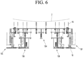
- FIG. 6 is a front view of the panel pop-up mechanism according to the present embodiment when the substrate is bent.
- the substrate chuck 11 may include a panel chuck 12 and a panel pop-up mechanism 13, as shown in FIG. 4 .
- the panel stage 5 may further include a table 14 having legs 14a, as shown in FIG. 4 , and the substrate chuck 11 may be placed on the table 14.
- the substrate chuck 11 may further include a mounting member 15 and a transfer mechanism 14b and 14c.
- the mounting member 15 may be placed on the table 14, and a panel chuck mounting portion 15a on which the panel chuck 12 is mounted may be formed on the mounting member 15.
- the panel chuck mounting portion 15a may be formed to protrude from the upper surface of the mounting member 15.
- the panel chuck mounting portion 15a may have an opening or transparent portion formed in the center.
- the panel chuck 12 may be mounted on the panel chuck mounting portion 15a in an area close to the edge.
- the mounting member 15 may be arranged to be horizontally movable on the table 14.
- the transfer mechanism 14b and 14c such as a motor for moving the mounting member 15 may be mounted on the table 14.
- the transfer mechanism 14b and 14c such as a motor may include a left-right transfer mechanism that may move the mounting member 15 in the left-right direction X.
- the transfer mechanism 14b and 14c such as a motor may include a back-and-forth transfer mechanism that may move the mounting member 15 in the front-back direction Y.
- the panel chuck 12 may be mounted on the panel chuck mounting portion 15a and supported on the mounting member 15.
- the panel chuck 12 may be placed on the table 14.
- a plurality of suction holes may be formed on the panel chuck 12.
- the panel chuck 12 may be a vacuum plate that absorbs the substrate 2.
- a suction tube may be connected to the panel chuck 12.
- the suction tube may be connected to the suction hole of the panel chuck 12 and the suction device.
- the substrate 2 placed on the upper surface of the panel chuck 12 may be absorbed by the panel chuck 12 by the suction tube and the suction device.
- the panel chuck 12 may be divided into multiple regions. A plurality of suction holes may be formed in each of the multiple regions. An example of the multiple regions may be 12 regions.
- the panel chuck 12 may flatly adsorb or air-float the substrate 2.
- the panel chuck 12 may be positioned above the vision sensor 26 and may cover the vision sensor 26 from the upper side.
- the panel chuck 12 may be formed of a ceramic series material or a reinforced glass material.
- An example of the panel chuck 12 may be a Pyrex material.
- the panel chuck 12 may be transparent or translucent.
- the panel chuck 12 satisfies the transparency condition that allows the precision vision of the vision sensor 26 to pass through.
- the panel chuck 12 is applied with a Pyrex material, and the upper surface of the Pyrex may be polished.
- a pin through hole through which a pin 16 of the panel pop-up mechanism 13 penetrates may be formed in the panel chuck 12.
- the pin through hole may be spaced apart from the suction hole that suctions the substrate 2.
- the panel pop-up mechanism 13 may be a mechanism that may elevate or bend the substrate 2 mounted on the panel chuck 12.
- the panel pop-up mechanism 13 may include the pin 16, as shown in FIGS. 4 to 6 .
- the pin 16 may be positioned so as to be liftable on the panel chuck 12.
- the pin 16 may protrude upwardly from the panel chuck 12 through the pin through hole of the panel chuck 12 and may be lowered into the pin through hole of the panel chuck 12. This pin 16 may elevate the substrate 2 positioned on the panel chuck 12.
- An upper end 16a of the pin 16 may be curved.
- the upper end 16a of the pin 16 may be a contact surface that comes into contact with the substrate 2, and when the upper end 16a of the pin 16 is curved, the contact area between the substrate 2 and the pin 16 may be minimized.
- the panel pop-up mechanism 13 may include a driving source 17 such as a motor or cylinder that raises and lowers the pin 16.
- the driving source 17 may be configured as a servo motor that raises and lowers the pin 16, and may control the pin 16 in the Z-axis servo.
- the driving source 17 and the pin 16 may be connected by a power transmission member.
- the power transmission member may convert the rotational motion of the driving source 17 into the up-and-down linear motion of the pin 16, and may include a gear, a link, a screw, a belt, or the like.
- the power transmission member is not limited to the type as long as it may convert the rotational motion of the driving source 17 into the up-and-down linear motion of the pin 16.
- the panel pop-up mechanism 13 may include a pop-up base 18.
- the pop-up base 18 may support the panel pop-up mechanism 13.
- the pop-up base 18 may be placed on the ground.
- a pop-up frame 19 may be placed on the pop-up base 18.
- the pop-up frame 19 may be a combination of multiple members.
- the panel pop-up mechanism 13 may include a plurality of pins 16 and a plurality of driving sources 17.
- the panel pop-up mechanism 13 may include a plurality of pop-up units 13A, 13B, 13C, 13D, 13E, 13F, 13G, and 13H including the pin 16 and the driving source 17.
- the panel pop-up mechanism 13 may lift and lower eight areas of the substrate 2 differently.
- the plurality of pop-up units 13A, 13B, 13C, 13D, 13E, 13F, 13G, and 13H may control multiple pop-up units 13A, 13B, 13C, 13D, 13E, 13F, 13G, and 13H so that the upper height of some of the multiple pins 16 is different from the upper height of the remaining pins 16.
- the plurality of pop-up units 13A, 13B, 13C, 13D, 13E, 13F, 13G, and 13H may include outer pop-up units 13A, 13B, 13C, 13D, 13E, and 13F that include the pin 16a that contacts an area close to the edge of the substrate 2, and inner pop-up units 13G and 13H that include the pin 16a that contacts an area close to the center of the substrate 2.
- the pin 16 elevation height of the inner pop-up units 13G and 13H may be lower than the pin 16 elevation height of the outer pop-up units 13A, 13B, 13C, 13D, 13E, and 13F.
- the substrate 2 may be supported in a shape in which the height of the edge is higher than the height of the center, and the substrate 2 may be bent in a shape close to a U-shape.
- FIG. 7 is a perspective view of an aligner according to the present embodiment.
- the substrate chuck 11 may further include an aligner 20 for aligning the substrate 2.
- the aligner 20 may be provided in multiple numbers on the panel chuck 12.
- the plurality of aligners 20 may be arranged around the panel chuck 12, as shown in FIG. 4 .
- the plurality of aligners 20 may include a left aligner 20A and a right aligner 20B spaced apart in the left-right direction X and may include a front aligner 20C and a rear aligner 20D spaced apart in the front-back direction Y.
- the plurality of aligners 20 may be spaced apart from each other.
- a panel chuck receiving space S in which the panel chuck 12 is received may be formed between the left aligner 20A, the right aligner 20B, the front aligner 20C, and the rear aligner 20D.
- the aligner 20 may include a urethane roller 21, a link 22 on which the urethane roller 21 is arranged, and a motor 25 that operates the link 22.
- the outer peripheral surface of the urethane roller 21 may be in contact with the peripheral surface of the substrate 2 or the peripheral surface of the panel chuck 12.
- the link 22 may include a main link 23 arranged along the periphery of the panel chuck 12, and a plurality of sub-links 24 arranged on the main link 23 and facing the periphery of the panel chuck 12.
- the urethane roller 21 may be rotatably mounted on the sub-link 24.
- the urethane roller 21 may be spaced apart from the main roller 23.
- An example of the motor 25 may be a servo motor and may be servo controlled.
- the motor 25 may rotate or linearly move the link 22.
- Each of the substrate 2 and the panel chuck 12 may include four peripheries left periphery, right periphery, front periphery, rear periphery.
- the urethane roller 21 of each of the plurality of aligners 20 may be in contact with the circumference of the substrate 2 or the circumference of the panel chuck 12.
- the plurality of aligners 20 include the urethane roller 21, when the substrate 2 is aligned by the plurality of aligners 20, damage to the substrate 2 made of glass may be minimized.
- the plurality of aligners 20 may align four circumferential surfaces with respect to the mounting position of the substrate 2, and the substrate 2 may be individually aligned on four surfaces, and the alignment position may be adjusted by servo control.
- FIG. 8 is a perspective view illustrating a panel vision alignment mechanism according to the present embodiment.
- the apparatus for manufacturing a micro-LED display may include a panel vision alignment mechanism 27 including a vision sensor 26.
- the vision alignment mechanism 27 may simultaneously photograph the alignment key of the substrate 2 and the alignment key of the donor 1 from the lower portion of the substrate 2, and the apparatus for manufacturing a micro-LED display may simultaneously correct the donor 1 and the substrate 2.
- the vision sensor 26 may include a high-resolution camera sensor, and may be adjusted to a right angle of within 5 ⁇ m.
- the vision alignment mechanism 27 may include four high-resolution camera sensors as a set, and may be configured to individually drive one set of the four high-resolution camera sensors in the X-axis, Y-axis, and Z-axis.
- the vision alignment mechanism 27 may include a vision sensor mounter 28 having the vision sensor 26 installed therein, and may include an X-axis driving unit 29a capable of driving the vision sensor mounter 28 along the X-axis, a Y-axis driving unit 29b capable of driving the vision sensor mounter 28 along the Y-axis, and a Z-axis driving unit 29c capable of driving the vision sensor mounter 28 along the Z-axis.
- FIG. 9 is a perspective view of a transfer head according to the present embodiment
- FIG. 10 is a perspective view illustrating an adsorption plate of a transfer head according to the present embodiment
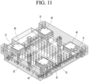
- FIG. 11 is a perspective view illustrating an adsorption plate and a light source of a transfer head according to the present embodiment
- FIG. 12 is a perspective view illustrating a drive module of a transfer head according to the present embodiment.
- the transfer head 7 may include a suction plate 30 to which the donor 1 is sucked.
- a light source 40 that irradiates light toward the donor 1 may be placed on the suction plate 30.
- a light source receiving portion 31 in which a light source 40 is inserted and received may be formed on the suction plate 30.
- the suction plate 30 may be a combination of multiple members, and the suction plate 30 may include a suction plate 32 and a fixed plate 34.
- the suction plate 30 may have an overall hexahedral shape.
- the suction plate 32 may have a plurality of suction holes 33 (see FIG. 11 ).
- the suction holes 33 may be formed through the suction plate 32.
- the upper surface of the donor 1 may be absorbed by the lower surface of the suction plate 32.
- the suction hole 33 has a diameter capable of absorbing the donor 1.
- the suction plate 32 itself be configured to ensure the flatness of the donor 1 when absorbing the donor 1.
- An example of the diameter of the suction hole 33 may be 0.7 mm.
- the suction plate 32 may be a vacuum plate in which a plurality of suction holes 33 having a diameter of 0.7 mm are formed.
- the light source receiving portion 31 may be formed in the suction plate 32.
- the light source receiving portion 31 may be formed in a sunken shape in the suction plate 32, as illustrated in FIG. 11 .
- the light source receiving portion 31 may be in the form of an upper surface and a side surface open to the suction plate 32.
- a plurality of light source receiving portions 31 may be formed on the suction plate 32, and the plurality of light source receiving portions 31 may be formed to be spaced apart from each other.
- the light source receiving portion 31 may be formed to be spaced apart from the suction hole 33.
- the suction plate 32 is configured to have a structure in which light generated from the light source 40 may be irradiated downward, and the suction plate 32 may have an opening formed on the lower side of the light source receiving portion 31 through which light is transmitted, or a transparent portion may be arranged.
- the light source 40 may be configured as a white back light that allows the vision sensor 26 to simultaneously recognize the alignment key of the substrate 2 and the alignment key of the donor 1.
- the light source 40 may be closer to the donor 1, and the vision sensor 26 may sense the alignment key of the donor 1 and the alignment key of the substrate 2 with greater reliability.
- a plurality of light sources 40 may be provided on the suction plate 32. It is preferable that at least four light sources 40 are provided.
- the fixed plate 34 may be placed on the upper surface of the suction plate 32, as shown in FIG. 10 .
- the fixed plate 34 may cover the upper surface of the suction plate 32.
- the fixed plate 34 may be fastened to the suction plate 32 with a fastening member such as a screw.
- the fixed plate 34 may cover the light source receiving portion 31.
- the light source 40 may be hidden by the fixed plate 34.
- the fixed plate 34 may be connected to the connecting bracket 60 (see FIG. 9 ) of the transfer head 7.
- the driving module 50 may be arranged on the upper side of the connecting bracket 60 and may be connected to the connecting bracket 60.
- An output shaft 56 of the driving module 50 may be connected to the connecting bracket 60.
- the driving module 50 may have an X-axis driving source 51, a Y-axis driving source 52, a ⁇ -axis driving source 53, a Tx-axis driving source 54, and a Ty-axis driving source 55, as shown in FIG. 12 .
- the driving module 50 may be a 5-axis module capable of moving and rotating the connecting bracket 60 along 5 axes.
- the drive module 50 may move the output shaft 56 along the X-axis, Y-axis, and rotate the Tx-axis, Ty-axis, and ⁇ -axis.
- the X-axis movement may be the left-right direction X movement of the output shaft 56, and the Y-axis movement may be the front-back direction Y movement.
- the ⁇ -axis rotation may be the rotation around the vertical first center axis of the output shaft 56.
- the Tx-axis rotation may be the rotation of the output shaft 56 around the horizontal second center axis, but the second center axis may be the center axis of the left-right direction X.
- the Ty-axis rotation may be the rotation of the output shaft 56 around the horizontal third center axis, but the third center axis may be the center axis of the front-back direction Y.
- the driving module 50 may be spaced apart from the suction plate 50 in the upper side of the suction plate 30 in the up-down direction Z, and a gap G may be formed between the suction plate 30 and the driving module 50.
- the upper part of the connecting bracket 60 may be connected to the driving module 50, and the lower part may be connected to the suction plate 30.
- the connecting bracket 60 may be long in the vertical direction, and the driving module 50 and the suction plate 30 may be spaced apart from each other in the vertical direction by the connecting bracket 60.
- the upper part of the connecting bracket 60 may be connected to the output shaft 56 of the driving module 50.
- the lower part of the connecting bracket 60 may be connected to the fixed plate 34.
- the lifting plate 70 may be placed on the upper part of the driving module 50.
- the driving module 50 may be installed on the lifting plate 70 so as to be hung on the lifting plate 70.
- the size of the lifting plate 70 may be larger than the size of the driving module 50, and the driving module 50 may be protected by the lifting plate 70.
- the lifting mechanism 80 may be a Z-axis mover that may move the driving module 50 in the Z-axis direction.
- the lifting mechanism 80 may be connected to the lifting plate 70 and may elevate the lifting plate 70.
- the lifting mechanism 80 is not limited to its type as long as it has a configuration that may lift the lifting plate 70.
- An example of the lifting mechanism 80 may include a lifting guide 81, a lifting plate 82 guided by the lifting guide 81, a connecting member 83 connecting the lifting plate 82 and the lifting plate 70, and a lifting driving source 84 that generates a driving force to lift the lifting plate 82.
- the lifting guide 81 may be an LM guide formed long in the vertical direction.
- the lifting guide 81 may be mounted on a transfer head mounter.
- An example of the lifting driving source 84 may be a servo motor.
- the transfer head 7 may further include a displacement sensor 90.
- the displacement sensor 90 may calculate the height or inclination between the substrate 2 and the donor 1.
- An example of the displacement sensor 90 may be a laser displacement sensor, and a spectral sensor with a resolution of 0.25 ⁇ m may be applied to the laser displacement sensor.
- the displacement sensor 90 may have a manual stage structure that allows precise adjustment for the X-axis, Y-axis, and Z-axis.
- the displacement sensor 90 may irradiate a laser to the donor 1 or the substrate 2 through the opening of the suction plate 30 from the upper side of the suction plate 30, and may sense the distance between the donor 1 and the substrate 2 or the degree of inclination of the donor 1 or the substrate 2.
- the displacement sensor 90 may be accommodated in the gap G between the suction plate 30 and the driving module 50, and may be protected by the suction plate 30 and the driving module 50.
- the displacement sensor 90 may be positioned around the connecting bracket 60, and a plurality of displacement sensors 90 may be arranged around the connecting bracket 60. A plurality of displacement sensors 90 may be arranged spaced apart from each other around the connecting bracket 60.
- FIG. 13 is a perspective view illustrating a lifting mechanism of a transfer head according to the present embodiment.
- the lifting mechanism 80 of the transfer head 7 may further include a screw 85 and a lifting connector 86.
- the screw 85 may be connected to a lifting drive source 84.
- the screw 85 may be formed to be long in the up-down direction Z and may be connected to a rotational axis of the lifting drive source 84.
- the lifting connector 86 may be lifted along the screw 85 and connected to the lifting plate 82.
- the lifting drive source 84 When the lifting drive source 84 is driven, if the screw 85 rotates, the lifting connector 86 may be lifted along the outer circumference of the screw 85.
- the lifting mechanism 80 of the transfer head 7 may further include an encoder scale 87.
- the encoder scale 87 may be a scale of a full closed control method to control within 0.1 ⁇ m through a precision scale, and may be precisely driven in the Z-axis direction of the suction plate 30.
- the lifting mechanism 80 of the transfer head 7 may further include a photo sensor 88.
- the photo sensor 88 may sense the lifting plate 82, and the apparatus for manufacturing a micro-LED display may control the lifting height of the lifting plate 82.
Landscapes
- Container, Conveyance, Adherence, Positioning, Of Wafer (AREA)
- Led Device Packages (AREA)
- Devices For Indicating Variable Information By Combining Individual Elements (AREA)
Abstract
Description
- The present disclosure relates to an apparatus for manufacturing a micro-LED display.
- Recently, display devices with good characteristics such as thinness and flexibility are being developed in the display technology field. The major displays currently commercialized are represented by LCD (Liquid Crystal Display) and AMOLED (Active Matrix Organic Light Emitting Diodes).
- However, LCD has problems such as slow response time and difficulty in implementing flexibility, and AMOLED has vulnerabilities such as short lifespan and poor mass production yield.
- Meanwhile, light-emitting diodes (LEDs) are well-known semiconductor light-emitting elements that convert current into light. Starting with the commercialization of red LEDs using GaAsP compound semiconductors, they have been used as light sources for display images in electronic devices including information and communication devices along with green LEDs of the GaP:N series. Therefore, a method can be proposed to solve the above problems by implementing a display (i.e., LED display) using the above semiconductor light-emitting elements. These light-emitting diodes have various advantages compared to filament-based light-emitting devices, such as long life, low power consumption, excellent initial driving characteristics, and high vibration resistance.
- Meanwhile, micro-LEDs (µLEDs) with a size of 10 to 100 micrometers (µm), which are 1/10th the length and 1/100th the area of general light-emitting diode (LED) chips, are gradually increasing.
- These micro-LEDs (µLEDs) have the advantages of faster response speed, lower power, higher brightness, and not breaking when applied to displays when bent, compared to conventional LEDs.
- A display device using the micro-LED (µLED) can perform an LED chip transfer process in which an LED chip is provided to a donor and then the LED chip provided to the donor is transferred back to a substrate.
- After the LED chip transfer process is completed, a donor stripping process in which the donor is removed from the substrate can be performed.
- The present embodiment provides a micro-LED display manufacturing device in which a vision sensor can simultaneously photograph a substrate and a donor, and the substrate and the donor can be aligned together.
- An apparatus for manufacturing a micro-LED display according to an aspect of embodiments may include a substrate chuck on which a substrate is mounted; a transfer head having an adsorption plate on which a donor is adsorbed, transferring an LED chip transferred to the donor to the substrate; and a vision sensor disposed below the substrate chuck, wherein a light source irradiating light toward the donor is disposed on the adsorption plate.
- The substrate chuck may include a panel chuck having a plurality of suction holes formed therein; a pin disposed to be liftable on the panel chuck and lifting the substrate; and a plurality of aligners for aligning the substrate.
- The panel chuck may be disposed above the vision sensor, and the panel chuck may be made of a Pyrex material.
- The pin may have a curved upper surface.
- The plurality of aligners may include a left aligner and a right aligner spaced apart in a left-right direction; and a front-side aligner and a right-side aligner spaced apart in a front-back direction.
- The aligner may include a urethane roller; a link on which the urethane roller is arranged; and a motor for driving the link.
- The suction plate may be formed with a light source receiving portion into which the light source is inserted and received.
- The suction plate may include a suction plate having a plurality of suction holes and in which the light source receiving portion is formed spaced apart from the suction hole; and a fixing plate arranged on the upper surface of the suction plate and covering the light source receiving portion.
- The transfer head may further include a driving module; a connecting bracket connected to the driving module and having a lower portion connected to the suction plate; a lifting plate arranged on the upper portion of the driving module; and a lifting mechanism for lifting the lifting plate.
- The driving module may have an X-axis driving source, a Y-axis driving source, a Θ-axis driving source, a Tx-axis driving source, and a Ty-axis driving source, and is a 5-axis module that moves the connecting bracket along the X-axis and Y-axis and rotates connecting bracket along the Tx-axis, Ty-axis, and Θ-axis.
- The transfer head may further include a displacement sensor for calculating a height or inclination between the substrate and the donor.
- A gap may be formed between the suction plate and the driving module, and the displacement sensor is received in the gap.
- According to this embodiment, a light source installed on the suction plate can backlight the donor absorbed by the suction plate, and a vision sensor on the lower side of the substrate can reliably recognize the align key of the substrate and the align key of the donor at the same time.
- In addition, since the light source is placed on the suction plate, inspection and repair of the light source are easy.
- In addition, since the panel chuck is made of Pyrex material, the reliability of the vision sensor can be high.
- In addition, since the upper part of the pin is curved, the contact area between the substrate and the pin can be minimized.
- In addition, since the substrate chuck includes a plurality of aligners that align the substrate, the substrate and the donor can be aligned at the same time, and the plurality of aligners can correct the alignment key of the substrate and the alignment key of the donor at the same time.
- In addition, since the aligner includes a urethane roller made of urethane material, damage to the substrate caused by the aligner can be minimized. In addition, the light source is inserted and received in the light source receiving portion formed on the suction plate, and when the light source protrudes, the light source can be protected more reliably.
- In addition, the light source received in the suction plate can be protected by the fixing plate, and the light from the light source can be reliably irradiated to the donor.
- In addition, since the displacement sensor is received in the gap between the suction plate and the driving module, damage to the displacement sensor can be minimized.
-
-
FIG. 1 is a perspective view of an apparatus for manufacturing a micro-LED display according to the present embodiment. -
FIG. 2 is a plan view of an apparatus for manufacturing a micro-LED display according to the present embodiment. -
FIG. 3 is a diagram illustrating a transfer process by an apparatus for manufacturing a micro-LED display according to the present embodiment. -
FIG. 4 is a perspective view of a panel stage according to the present embodiment. -
FIG. 5 is a perspective view of a panel pop-up mechanism according to the present embodiment. -
FIG. 6 is a front view of the panel pop-up mechanism according to the present embodiment when the substrate is bent. -
FIG. 7 is a perspective view of an aligner according to the present embodiment. -
FIG. 8 is a perspective view illustrating a panel vision alignment mechanism according to the present embodiment. -
FIG. 9 is a perspective view of a transfer head according to the present embodiment. -
FIG. 10 is a perspective view illustrating an adsorption plate of a transfer head according to the present embodiment. -
FIG. 11 is a perspective view illustrating an adsorption plate and a light source of a transfer head according to the present embodiment. -
FIG. 12 is a perspective view illustrating a drive module of a transfer head according to the present embodiment. -
FIG. 13 is a perspective view illustrating a lifting mechanism of a transfer head according to the present embodiment. - Hereinafter, specific embodiments of the present disclosure will be described in detail with drawings.
-
FIG. 1 is a perspective view of an apparatus for manufacturing a micro-LED display according to the present embodiment,FIG. 2 is a plan view of an apparatus for manufacturing a micro-LED display according to the present embodiment, andFIG. 3 is a diagram illustrating a transfer process by an apparatus for manufacturing a micro-LED display according to the present embodiment. - The apparatus for manufacturing a micro-LED display may transfer an
LED chip 3 provided to a donor (1, seeFIG. 3 ) to asubstrate 2. The apparatus for manufacturing a micro-LED display may be a transfer device that transfers theLED chip 3 to thesubstrate 2. - The apparatus for manufacturing a micro-LED display may include a
panel stage 5, adonor loader 6, atransfer head 7, a detachinghead 8, and adonor unloader 9, as shown inFIGS. 1 and2 . - The
donor 1 may be an interposer provided with anLED chip 3 on one side. Thedonor 1 may be loaded onto thesubstrate 2 to transfer theLED chip 3 onto thesubstrate 2. Thedonor 1 is preferably formed of a transparent material or a translucent material. - The
donor 1 may be provided with an align key, and may be loaded into the apparatus for manufacturing a micro-LED display while the align key is provided. - The drawing symbol DI illustrated in
FIG. 2 indicates a direction in which thedonor 1 is loaded onto thesubstrate 2, and the drawing symbol DO illustrated inFIG. 2 indicates a direction in which thedonor 1 is unloaded from thesubstrate 2. - The
substrate 2 may be mounted on thepanel stage 5, as illustrated inFIGS. 1 and2 . - An example of the
substrate 2 may include apanel 2a and an adhesive 2b formed on an upper surface of thepanel 2a, as shown inFIG. 3 . - An example of the
panel 2a may be a CID panel. The material of thepanel 2a may be a glass material. It is preferable that thepanel 2a is formed of a transparent material or a translucent material. - A plurality of
adhesives 2b may be formed on the upper surface of thepanel 2a, and the plurality ofadhesives 2b may be separated from each other. - Among the
substrates 2, thepanel 2a may be mounted on thepanel stage 5, and thepanel 2a may be chucked to thepanel stage 5. - An example of the
substrate 2 may further include alight guide 2c. Thelight guide 2c may be a partition wall that partitions theLED chip 3. Thelight guide 2c may be a reflective layer or reflective sheet that reflects the light of theLED chip 3. - When the
substrate 2 is mounted on thepanel stage 5, thelight guide 2c may be formed in a plurality of numbers on the upper surface of thepanel 2a, and the plurality ofadhesives 2b may be spaced apart from each other by thelight guide 2c. When a plurality ofLED chips 3 is transferred to thesubstrate 2, thelight guide 2c may be positioned between themultiple LED chips 3. - An align key may be provided on the
substrate 2, and the substrate may be loaded onto thepanel stage 5 while the align key is provided. - The drawing symbol SI illustrated in
FIG. 2 indicates the direction in which thesubstrate 2 is loaded onto thepanel stage 5, and the drawing symbol SO illustrated inFIG. 2 indicates the direction in which thesubstrate 2 is unloaded on thepanel stage 5. - The
substrate 2 may be advanced in the front-back direction Y above thepanel stage 5 as shown inFIG. 2 , and may be retracted in the front-back direction Y above thepanel stage 5. - A plurality of
LED chips 3 may be provided on thedonor 1. TheLED chip 3 provided on thedonor 1 may be a micro-LED chip, and a plurality of micro-LED chips may be provided on one surface of thedonor 1. The LED chips 3 may be loaded into the apparatus for manufacturing a micro-LED display while being provided on the bottom surface of thedonor 1. - Hereinafter, the configuration of the apparatus for manufacturing a micro-LED display will be described.
- The
panel stage 5 may include asubstrate chuck 11 on which thesubstrate 2 is mounted. - The
substrate chuck 11 may be positioned between thedonor loader 6 and thedonor unloader 9 in the left-right direction X, and may horizontally chuck thesubstrate 2. As shown inFIGS. 1 and2 , thesubstrate 2 may receive theLED chip 3 from thedonor 1 while being placed on thesubstrate chuck 11. - The
panel stage 5 may align the position of thesubstrate 2. Thepanel stage 5 may simultaneously align thesubstrate 2 and thedonor 1. Thepanel stage 5 may absorb thesubstrate 2 and may absorb a large substrate. - The
panel stage 5 may be formed long in the left-right direction X. Thepanel stage 5 may be formed long in the front-back direction Y. The left-right direction X length of thepanel stage 5 may be longer than the front-back direction Y length of thepanel stage 5. Thepanel stage 5 may have a rectangular shape that is elongated in the left-right direction X when viewed from above. - The
donor loader 6 may load thedonor 1. Thedonor loader 6 may load thedonor 1 to thetransfer head 7. - The
donor loader 6 may be placed on thepanel stage 5, and thedonor loader 6 may be eccentrically placed on one side (for example, the right side) of the left and right sides of thepanel stage 6. Thedonor loader 6 may be spaced apart from thesubstrate chuck 11 and thedonor unloader 9 in the left-right direction X. - The
donor loader 6 may include a reverser that may reverse thedonor 1. Thedonor loader 6 may include a rotating device that may rotate thedonor 1. Thedonor loader 6 may reverse and rotate thedonor 1. - The
donor loader 6 may include a barcode recognition unit that recognizes a barcode formed on thedonor 1, and may recognize the barcode while tracking thedonor 1. Thedonor loader 6 may align the position of thedonor 1. Thedonor loader 6 may align thedonor 1 prior to thetransfer head 7 adsorbing thedonor 1. - The
donor 1 may be adsorbed on an adsorption plate 30' (Vacuum plate) as shown in a ofFIG. 3 , and may be sensed by a vision sensor 20'. The vision sensor may perform a pre-vision align that senses theLED chip 3 provided on the bottom surface of thedonor 1 and thedonor 1. - As shown in (a) of
FIG. 3 , the suction plate 30' may be thesuction plate 30 of thetransfer head 7, or may be provided separately from thesuction plate 30 of thetransfer head 7. - As shown in (a) of
FIG. 3 , a vision sensor 26' may be avision sensor 26 arranged on the lower side of thesubstrate chuck 11, or may be provided separately from thevision sensor 26 arranged on the lower side of thesubstrate chuck 11. - The
transfer head 7 may transfer theLED chip 3 provided on thedonor 1 to thesubstrate 2. - After receiving the
donor 1 of thedonor loader 6, thetransfer head 7 may transfer theLED chip 3 to thesubstrate 2. - The
transfer head 7 may absorb thedonor 1 and lift and lower the absorbeddonor 1. Thetransfer head 7 may be movably arranged on thepanel stage 5. Thetransfer head 7 may be arranged to move in the left-right direction X on thepanel stage 5. - The
transfer head 7 may correct the parallelism between thedonor 1 and thesubstrate 2. Thetransfer head 7 may be controlled in the Z-axis (up-down direction) for each bonding section. - The
transfer head 7 may be moved to the upper side of thedonor loader 6 and may be moved to the upper side of thesubstrate chuck 11. - The
transfer head 7 may move thedonor 1 to the upper position of thesubstrate 2, as shown in (b) ofFIG. 3 , and may lower thedonor 1 to thesubstrate 2 from the upper position of thesubstrate 2. Thetransfer head 7 may adjust the angle of thedonor 1, and thedonor 1 may be adjusted to be parallel to thesubstrate 2. - A plurality of transfer heads 7 may be provided. The plurality of transfer heads 7 may be arranged in a row. The plurality of transfer heads 7 may be arranged in a row in the front-back direction Y.
- The apparatus for manufacturing a micro-LED display may include a transfer head mounter on which the plurality of transfer heads 7 is mounted, and the plurality of transfer heads 7 may be arranged in a row in the front-back direction Y on the transfer head mounter.
- The apparatus for manufacturing a micro-LED display may further include a transfer head mounter moving mechanism that moves the transfer head mounter in the left-right direction X. The transfer head mounter moving mechanism may be mounted on the
panel stage 2. The transfer head mounter moving mechanism may include a driving source such as a motor, and at least one power transmission member connected to the driving source and the transfer head mounter. The transfer head mounter moving mechanism may include a linear guide that guides the power transmission member. - The detaching
head 8 may detach thedonor 1 on which theLED chip 3 is transferred to thesubstrate 2. The detachinghead 8 may remove thedonor 1 from which theLED chip 3 is separated (i.e., transfer is completed). The detachinghead 8 may remove thedonor 1 from which theLED chip 3 is separated (i.e., transfer is completed) by adsorbing/gripping thedonor 1. The detachinghead 8 may transport thedonor 1 located on the upper side of thesubstrate 2 to thedonor unloader 9. - The detaching
head 8 may be movably arranged on thepanel stage 5. Thetransfer head 7 may be arranged to move in the left-right direction X on thepanel stage 5. - The detaching
head 8 may be moved to the upper side of thedonor unloader 9. The detachinghead 8 may transfer thedonor 1 on the upper side of thesubstrate chuck 11 to thedonor unloader 9. - A plurality of detaching
heads 8 may be provided. The plurality of detachingheads 8 may be arranged in a row. The plurality of detachingheads 8 may be arranged in a row in the front-back direction Y. - The apparatus for manufacturing a micro-LED display may include a detaching head mounter on which the plurality of detaching
heads 8 is mounted, and the plurality of detachingheads 8 may be arranged in a row in the front-back direction Y on the detaching head mounter. - The apparatus for manufacturing a micro-LED display may further include a detaching head mounter moving mechanism that moves the detaching head mounter in the left-right direction X. The detaching head mounter moving mechanism may be mounted on the
panel stage 2. The detaching head mounter moving mechanism may include a driving source such as a motor, and at least one power transmission member connected to the driving source and the detaching head mounter. The detaching head mounter moving mechanism may include a linear guide that guides the power transmission member. - The
donor unloader 9 may unload thedonor 1. - The
donor unloader 9 may be placed on thepanel stage 5, and thedonor unloader 9 may be eccentrically placed on the other side for example, the left side of thepanel stage 6. Thedonor unloader 9 may be spaced apart from thesubstrate chuck 11 and thedonor unloader 9 in the left-right direction X. - The
donor unloader 9 may align thedonor 1. Thedonor unloader 9 may include a reverser that may reverse thedonor 1. Thedonor unloader 9 may include a rotation device that may rotate thedonor 1. Thedonor unloader 9 may reverse and rotate thedonor 1. - The apparatus for manufacturing a micro-LED display may include a vision sensor 20 (see (b) of
FIG. 3 ) placed under thesubstrate chuck 11. - The
vision sensor 26 may capture an image of thesubstrate 2 and an image of theLED chip 3 at a lower position of thesubstrate 2 mounted on thesubstrate chuck 11. Thevision sensor 26 may capture an image of theLED chip 3 located on the lower surface of thedonor 1 through an area opening or transparent portion of thesubstrate chuck 11 through which light may pass, and may capture thepanel 2. - The apparatus for manufacturing a micro-LED display may correct the position of the
LED chip 3, the angle of thedonor 1, or the position of thesubstrate 2 according to the sensing result of thevision sensor 26, and may transfer theLED chip 3 to the correct position on thesubstrate 2. - The apparatus for manufacturing a micro-LED display may be positioned on the upper side of the
substrate 2 as shown in (b) ofFIG. 3 after thesubstrate 2 is placed on thesubstrate chuck 11 of thepanel stage 5 as shown inFIG. 1 andFIG. 2 . Thereafter, thedonor 1 may be lowered to thesubstrate 2 as shown in (c) ofFIG. 3 to transfer theLED chip 3 to thesubstrate 2, especially the adhesive 2b, and theLED chip 3 may be adhered to thesubstrate 2 by the adhesive 2b, as shown in (d) ofFIG. 3 . Thereafter, thedonor 1 may be raised away from thesubstrate 2 as shown in (e) ofFIG. 3 and may be removed from thesubstrate 2. -
FIG. 4 is a perspective view of a panel stage according to the present embodiment.FIG. 5 is a perspective view of a panel pop-up mechanism according to the present embodiment, andFIG. 6 is a front view of the panel pop-up mechanism according to the present embodiment when the substrate is bent. - The
substrate chuck 11 may include apanel chuck 12 and a panel pop-upmechanism 13, as shown inFIG. 4 . - The
panel stage 5 may further include a table 14 havinglegs 14a, as shown inFIG. 4 , and thesubstrate chuck 11 may be placed on the table 14. - The
substrate chuck 11 may further include a mountingmember 15 and atransfer mechanism - The mounting
member 15 may be placed on the table 14, and a panelchuck mounting portion 15a on which thepanel chuck 12 is mounted may be formed on the mountingmember 15. The panelchuck mounting portion 15a may be formed to protrude from the upper surface of the mountingmember 15. The panelchuck mounting portion 15a may have an opening or transparent portion formed in the center. Thepanel chuck 12 may be mounted on the panelchuck mounting portion 15a in an area close to the edge. - The mounting
member 15 may be arranged to be horizontally movable on the table 14. Thetransfer mechanism member 15 may be mounted on the table 14. Thetransfer mechanism member 15 in the left-right direction X. Thetransfer mechanism member 15 in the front-back direction Y. - The
panel chuck 12 may be mounted on the panelchuck mounting portion 15a and supported on the mountingmember 15. Thepanel chuck 12 may be placed on the table 14. - A plurality of suction holes may be formed on the
panel chuck 12. Thepanel chuck 12 may be a vacuum plate that absorbs thesubstrate 2. - A suction tube may be connected to the
panel chuck 12. The suction tube may be connected to the suction hole of thepanel chuck 12 and the suction device. Thesubstrate 2 placed on the upper surface of thepanel chuck 12 may be absorbed by thepanel chuck 12 by the suction tube and the suction device. - The
panel chuck 12 may be divided into multiple regions. A plurality of suction holes may be formed in each of the multiple regions. An example of the multiple regions may be 12 regions. Thepanel chuck 12 may flatly adsorb or air-float thesubstrate 2. - The
panel chuck 12 may be positioned above thevision sensor 26 and may cover thevision sensor 26 from the upper side. - The
panel chuck 12 may be formed of a ceramic series material or a reinforced glass material. An example of thepanel chuck 12 may be a Pyrex material. Thepanel chuck 12 may be transparent or translucent. - It is preferable that the
panel chuck 12 satisfies the transparency condition that allows the precision vision of thevision sensor 26 to pass through. Thepanel chuck 12 is applied with a Pyrex material, and the upper surface of the Pyrex may be polished. - Meanwhile, a pin through hole through which a
pin 16 of the panel pop-upmechanism 13 penetrates may be formed in thepanel chuck 12. The pin through hole may be spaced apart from the suction hole that suctions thesubstrate 2. - The panel pop-up
mechanism 13 may be a mechanism that may elevate or bend thesubstrate 2 mounted on thepanel chuck 12. - The panel pop-up
mechanism 13 may include thepin 16, as shown inFIGS. 4 to 6 . Thepin 16 may be positioned so as to be liftable on thepanel chuck 12. Thepin 16 may protrude upwardly from thepanel chuck 12 through the pin through hole of thepanel chuck 12 and may be lowered into the pin through hole of thepanel chuck 12. Thispin 16 may elevate thesubstrate 2 positioned on thepanel chuck 12. - An
upper end 16a of thepin 16 may be curved. Theupper end 16a of thepin 16 may be a contact surface that comes into contact with thesubstrate 2, and when theupper end 16a of thepin 16 is curved, the contact area between thesubstrate 2 and thepin 16 may be minimized. - The panel pop-up
mechanism 13 may include a drivingsource 17 such as a motor or cylinder that raises and lowers thepin 16. The drivingsource 17 may be configured as a servo motor that raises and lowers thepin 16, and may control thepin 16 in the Z-axis servo. The drivingsource 17 and thepin 16 may be connected by a power transmission member. - The power transmission member may convert the rotational motion of the driving
source 17 into the up-and-down linear motion of thepin 16, and may include a gear, a link, a screw, a belt, or the like. The power transmission member is not limited to the type as long as it may convert the rotational motion of the drivingsource 17 into the up-and-down linear motion of thepin 16. - The panel pop-up
mechanism 13 may include a pop-up base 18. The pop-up base 18 may support the panel pop-upmechanism 13. The pop-up base 18 may be placed on the ground. - A pop-
up frame 19 may be placed on the pop-up base 18. The pop-up frame 19 may be a combination of multiple members. - The panel pop-up
mechanism 13 may include a plurality ofpins 16 and a plurality of drivingsources 17. - The panel pop-up
mechanism 13 may include a plurality of pop-upunits pin 16 and the drivingsource 17. - When the eight pop-up
units mechanism 13 may lift and lower eight areas of thesubstrate 2 differently. - The plurality of pop-up
units units multiple pins 16 is different from the upper height of the remaining pins 16. - The plurality of pop-up
units units pin 16a that contacts an area close to the edge of thesubstrate 2, and inner pop-upunits pin 16a that contacts an area close to the center of thesubstrate 2. - The
pin 16 elevation height of the inner pop-upunits pin 16 elevation height of the outer pop-upunits substrate 2 may be supported in a shape in which the height of the edge is higher than the height of the center, and thesubstrate 2 may be bent in a shape close to a U-shape. -
FIG. 7 is a perspective view of an aligner according to the present embodiment. - The
substrate chuck 11 may further include analigner 20 for aligning thesubstrate 2. Thealigner 20 may be provided in multiple numbers on thepanel chuck 12. - The plurality of
aligners 20 may be arranged around thepanel chuck 12, as shown inFIG. 4 . - The plurality of
aligners 20 may include aleft aligner 20A and aright aligner 20B spaced apart in the left-right direction X and may include afront aligner 20C and arear aligner 20D spaced apart in the front-back direction Y. - The plurality of
aligners 20 may be spaced apart from each other. A panel chuck receiving space S in which thepanel chuck 12 is received may be formed between theleft aligner 20A, theright aligner 20B, thefront aligner 20C, and therear aligner 20D. - The
aligner 20 may include aurethane roller 21, alink 22 on which theurethane roller 21 is arranged, and amotor 25 that operates thelink 22. - The outer peripheral surface of the
urethane roller 21 may be in contact with the peripheral surface of thesubstrate 2 or the peripheral surface of thepanel chuck 12. - The
link 22 may include amain link 23 arranged along the periphery of thepanel chuck 12, and a plurality ofsub-links 24 arranged on themain link 23 and facing the periphery of thepanel chuck 12. - The
urethane roller 21 may be rotatably mounted on the sub-link 24. Theurethane roller 21 may be spaced apart from themain roller 23. - An example of the
motor 25 may be a servo motor and may be servo controlled. Themotor 25 may rotate or linearly move thelink 22. - Each of the
substrate 2 and thepanel chuck 12 may include four peripheries left periphery, right periphery, front periphery, rear periphery. Theurethane roller 21 of each of the plurality ofaligners 20 may be in contact with the circumference of thesubstrate 2 or the circumference of thepanel chuck 12. - When the plurality of
aligners 20 include theurethane roller 21, when thesubstrate 2 is aligned by the plurality ofaligners 20, damage to thesubstrate 2 made of glass may be minimized. - The plurality of
aligners 20 may align four circumferential surfaces with respect to the mounting position of thesubstrate 2, and thesubstrate 2 may be individually aligned on four surfaces, and the alignment position may be adjusted by servo control. -
FIG. 8 is a perspective view illustrating a panel vision alignment mechanism according to the present embodiment. - The apparatus for manufacturing a micro-LED display may include a panel
vision alignment mechanism 27 including avision sensor 26. - The
vision alignment mechanism 27 may simultaneously photograph the alignment key of thesubstrate 2 and the alignment key of thedonor 1 from the lower portion of thesubstrate 2, and the apparatus for manufacturing a micro-LED display may simultaneously correct thedonor 1 and thesubstrate 2. - The
vision sensor 26 may include a high-resolution camera sensor, and may be adjusted to a right angle of within 5 µm. - The
vision alignment mechanism 27 may include four high-resolution camera sensors as a set, and may be configured to individually drive one set of the four high-resolution camera sensors in the X-axis, Y-axis, and Z-axis. - The
vision alignment mechanism 27 may include avision sensor mounter 28 having thevision sensor 26 installed therein, and may include anX-axis driving unit 29a capable of driving thevision sensor mounter 28 along the X-axis, a Y-axis driving unit 29b capable of driving thevision sensor mounter 28 along the Y-axis, and a Z-axis driving unit 29c capable of driving thevision sensor mounter 28 along the Z-axis. -
FIG. 9 is a perspective view of a transfer head according to the present embodiment,FIG. 10 is a perspective view illustrating an adsorption plate of a transfer head according to the present embodiment,FIG. 11 is a perspective view illustrating an adsorption plate and a light source of a transfer head according to the present embodiment, andFIG. 12 is a perspective view illustrating a drive module of a transfer head according to the present embodiment. - The
transfer head 7 may include asuction plate 30 to which thedonor 1 is sucked. - A
light source 40 that irradiates light toward thedonor 1 may be placed on thesuction plate 30. - A light
source receiving portion 31 in which alight source 40 is inserted and received may be formed on thesuction plate 30. - The
suction plate 30 may be a combination of multiple members, and thesuction plate 30 may include asuction plate 32 and a fixedplate 34. Thesuction plate 30 may have an overall hexahedral shape. - The
suction plate 32 may have a plurality of suction holes 33 (seeFIG. 11 ). The suction holes 33 may be formed through thesuction plate 32. The upper surface of thedonor 1 may be absorbed by the lower surface of thesuction plate 32. - It is preferable that the
suction hole 33 has a diameter capable of absorbing thedonor 1. - It is preferable that the
suction plate 32 itself be configured to ensure the flatness of thedonor 1 when absorbing thedonor 1. An example of the diameter of thesuction hole 33 may be 0.7 mm. Thesuction plate 32 may be a vacuum plate in which a plurality of suction holes 33 having a diameter of 0.7 mm are formed. - The light
source receiving portion 31 may be formed in thesuction plate 32. The lightsource receiving portion 31 may be formed in a sunken shape in thesuction plate 32, as illustrated inFIG. 11 . The lightsource receiving portion 31 may be in the form of an upper surface and a side surface open to thesuction plate 32. A plurality of lightsource receiving portions 31 may be formed on thesuction plate 32, and the plurality of lightsource receiving portions 31 may be formed to be spaced apart from each other. - The light
source receiving portion 31 may be formed to be spaced apart from thesuction hole 33. - The
suction plate 32 is configured to have a structure in which light generated from thelight source 40 may be irradiated downward, and thesuction plate 32 may have an opening formed on the lower side of the lightsource receiving portion 31 through which light is transmitted, or a transparent portion may be arranged. - The
light source 40 may be configured as a white back light that allows thevision sensor 26 to simultaneously recognize the alignment key of thesubstrate 2 and the alignment key of thedonor 1. - If the
light source 40 is not located below thesubstrate chuck 11 but above thedonor 1, thelight source 40 may be closer to thedonor 1, and thevision sensor 26 may sense the alignment key of thedonor 1 and the alignment key of thesubstrate 2 with greater reliability. - A plurality of
light sources 40 may be provided on thesuction plate 32. It is preferable that at least fourlight sources 40 are provided. - The fixed
plate 34 may be placed on the upper surface of thesuction plate 32, as shown inFIG. 10 . The fixedplate 34 may cover the upper surface of thesuction plate 32. The fixedplate 34 may be fastened to thesuction plate 32 with a fastening member such as a screw. - The fixed
plate 34 may cover the lightsource receiving portion 31. Thelight source 40 may be hidden by the fixedplate 34. - The fixed
plate 34 may be connected to the connecting bracket 60 (seeFIG. 9 ) of thetransfer head 7. - The
transfer head 7 may further include adriving module 50, a connectingbracket 60, a liftingplate 70, and alifting mechanism 80, as shown inFIG. 9 . - The driving
module 50 may be arranged on the upper side of the connectingbracket 60 and may be connected to the connectingbracket 60. Anoutput shaft 56 of the drivingmodule 50 may be connected to the connectingbracket 60. - The driving
module 50 may have anX-axis driving source 51, a Y-axis driving source 52, a θ-axis driving source 53, a Tx-axis driving source 54, and a Ty-axis driving source 55, as shown inFIG. 12 . The drivingmodule 50 may be a 5-axis module capable of moving and rotating the connectingbracket 60 along 5 axes. Thedrive module 50 may move theoutput shaft 56 along the X-axis, Y-axis, and rotate the Tx-axis, Ty-axis, and θ-axis. - The X-axis movement may be the left-right direction X movement of the
output shaft 56, and the Y-axis movement may be the front-back direction Y movement. - The θ-axis rotation may be the rotation around the vertical first center axis of the
output shaft 56. - The Tx-axis rotation may be the rotation of the
output shaft 56 around the horizontal second center axis, but the second center axis may be the center axis of the left-right direction X. - The Ty-axis rotation may be the rotation of the
output shaft 56 around the horizontal third center axis, but the third center axis may be the center axis of the front-back direction Y. - As shown in
FIG. 9 , the drivingmodule 50 may be spaced apart from thesuction plate 50 in the upper side of thesuction plate 30 in the up-down direction Z, and a gap G may be formed between thesuction plate 30 and the drivingmodule 50. - The upper part of the connecting
bracket 60 may be connected to thedriving module 50, and the lower part may be connected to thesuction plate 30. The connectingbracket 60 may be long in the vertical direction, and the drivingmodule 50 and thesuction plate 30 may be spaced apart from each other in the vertical direction by the connectingbracket 60. - The upper part of the connecting
bracket 60 may be connected to theoutput shaft 56 of the drivingmodule 50. The lower part of the connectingbracket 60 may be connected to the fixedplate 34. - The lifting
plate 70 may be placed on the upper part of the drivingmodule 50. The drivingmodule 50 may be installed on the liftingplate 70 so as to be hung on the liftingplate 70. The size of the liftingplate 70 may be larger than the size of the drivingmodule 50, and the drivingmodule 50 may be protected by the liftingplate 70. - The
lifting mechanism 80 may be a Z-axis mover that may move thedriving module 50 in the Z-axis direction. - The
lifting mechanism 80 may be connected to the liftingplate 70 and may elevate the liftingplate 70. Thelifting mechanism 80 is not limited to its type as long as it has a configuration that may lift the liftingplate 70. - An example of the
lifting mechanism 80 may include a liftingguide 81, a liftingplate 82 guided by the liftingguide 81, a connectingmember 83 connecting the liftingplate 82 and the liftingplate 70, and alifting driving source 84 that generates a driving force to lift the liftingplate 82. - The lifting
guide 81 may be an LM guide formed long in the vertical direction. - The lifting
guide 81 may be mounted on a transfer head mounter. - An example of the
lifting driving source 84 may be a servo motor. - The
transfer head 7 may further include adisplacement sensor 90. Thedisplacement sensor 90 may calculate the height or inclination between thesubstrate 2 and thedonor 1. - An example of the
displacement sensor 90 may be a laser displacement sensor, and a spectral sensor with a resolution of 0.25 µm may be applied to the laser displacement sensor. Thedisplacement sensor 90 may have a manual stage structure that allows precise adjustment for the X-axis, Y-axis, and Z-axis. - The
displacement sensor 90 may irradiate a laser to thedonor 1 or thesubstrate 2 through the opening of thesuction plate 30 from the upper side of thesuction plate 30, and may sense the distance between thedonor 1 and thesubstrate 2 or the degree of inclination of thedonor 1 or thesubstrate 2. - The
displacement sensor 90 may be accommodated in the gap G between thesuction plate 30 and the drivingmodule 50, and may be protected by thesuction plate 30 and the drivingmodule 50. - The
displacement sensor 90 may be positioned around the connectingbracket 60, and a plurality ofdisplacement sensors 90 may be arranged around the connectingbracket 60. A plurality ofdisplacement sensors 90 may be arranged spaced apart from each other around the connectingbracket 60. -
FIG. 13 is a perspective view illustrating a lifting mechanism of a transfer head according to the present embodiment. - The
lifting mechanism 80 of thetransfer head 7 may further include ascrew 85 and a liftingconnector 86. - The
screw 85 may be connected to alifting drive source 84. Thescrew 85 may be formed to be long in the up-down direction Z and may be connected to a rotational axis of the liftingdrive source 84. - The lifting
connector 86 may be lifted along thescrew 85 and connected to the liftingplate 82. - When the lifting
drive source 84 is driven, if thescrew 85 rotates, the liftingconnector 86 may be lifted along the outer circumference of thescrew 85. - The
lifting mechanism 80 of thetransfer head 7 may further include anencoder scale 87. - The
encoder scale 87 may be a scale of a full closed control method to control within 0.1 µm through a precision scale, and may be precisely driven in the Z-axis direction of thesuction plate 30. - The
lifting mechanism 80 of thetransfer head 7 may further include aphoto sensor 88. Thephoto sensor 88 may sense the liftingplate 82, and the apparatus for manufacturing a micro-LED display may control the lifting height of the liftingplate 82. - The above description is merely an example of the technical idea of the present disclosure, and those with ordinary knowledge in the technical field to which the present disclosure belongs may make various modifications and variations without departing from the essential characteristics of the present disclosure.
- Therefore, the embodiments disclosed in the present disclosure are not intended to limit the technical idea of the present disclosure, but to explain it, and the scope of the technical idea of the present disclosure is not limited by these embodiments.
- The protection scope of the present disclosure should be interpreted by the claims below, and all technical ideas within the equivalent scope should be interpreted as being included in the scope of the rights of the present disclosure.
Claims (12)
- An apparatus for manufacturing a micro-LED display, comprising:a substrate chuck on which a substrate is mounted;a transfer head having an adsorption plate on which a donor is adsorbed, transferring an LED chip transferred to the donor to the substrate; anda vision sensor disposed below the substrate chuck,wherein a light source irradiating light toward the donor is disposed on the adsorption plate.
- The apparatus according to claim 1, wherein the substrate chuck includes:a panel chuck having a plurality of suction holes formed therein;a pin disposed to be liftable on the panel chuck and lifting the substrate; anda plurality of aligners for aligning the substrate.
- The apparatus according to claim 1, wherein the panel chuck is disposed above the vision sensor, and
wherein the panel chuck is made of a Pyrex material. - The apparatus according to claim 1, wherein the pin has a curved upper surface.
- The apparatus according to claim 1, wherein the plurality of aligners includes:a left aligner and a right aligner spaced apart in a left-right direction; anda front-side aligner and a right-side aligner spaced apart in a front-back direction.
- The apparatus according to claim 2, wherein the aligner includes:a urethane roller;a link on which the urethane roller is arranged; anda motor for driving the link.
- The apparatus according to claim 1, wherein the suction plate is formed with a light source receiving portion into which the light source is inserted and received.
- The apparatus according to claim 7, wherein the suction plate includes:a suction plate having a plurality of suction holes and in which the light source receiving portion is formed spaced apart from the suction hole; anda fixing plate arranged on the upper surface of the suction plate and covering the light source receiving portion.
- The apparatus according to claim 1, wherein the transfer head further includes:a driving module;a connecting bracket connected to the driving module and having a lower portion connected to the suction plate;a lifting plate arranged on the upper portion of the driving module; anda lifting mechanism for lifting the lifting plate.
- The apparatus according to claim 1, wherein the driving module has a X-axis driving source, a Y-axis driving source, a Θ-axis driving source, a Tx-axis driving source, and a Ty-axis driving source, and is a 5-axis module that moves the connecting bracket along the X-axis and Y-axis and rotates connecting bracket along the Tx-axis, Ty-axis, and Θ-axis.
- The apparatus according to claim 1, wherein the transfer head further includes a displacement sensor for calculating a height or inclination between the substrate and the donor.
- The apparatus according to claim 11, wherein a gap is formed between the suction plate and the driving module, and
wherein the displacement sensor is received in the gap.
Applications Claiming Priority (1)
| Application Number | Priority Date | Filing Date | Title |
|---|---|---|---|
| PCT/KR2022/009261 WO2024005221A1 (en) | 2022-06-28 | 2022-06-28 | Micro-led display manufacturing device |
Publications (2)
| Publication Number | Publication Date |
|---|---|
| EP4546402A1 true EP4546402A1 (en) | 2025-04-30 |
| EP4546402A4 EP4546402A4 (en) | 2025-10-01 |
Family
ID=89382552
Family Applications (1)
| Application Number | Title | Priority Date | Filing Date |
|---|---|---|---|
| EP22949514.8A Pending EP4546402A4 (en) | 2022-06-28 | 2022-06-28 | Apparatus for producing a micro-LED display |
Country Status (5)
| Country | Link |
|---|---|
| US (1) | US20250393351A1 (en) |
| EP (1) | EP4546402A4 (en) |
| KR (1) | KR20250021560A (en) |
| CN (1) | CN119487624A (en) |
| WO (1) | WO2024005221A1 (en) |
Family Cites Families (8)
| Publication number | Priority date | Publication date | Assignee | Title |
|---|---|---|---|---|
| JP2009295853A (en) * | 2008-06-06 | 2009-12-17 | Sony Corp | Element transfer device, element transfer method, and method of manufacturing display device |
| KR20130020243A (en) * | 2011-08-19 | 2013-02-27 | 엘지디스플레이 주식회사 | Alignment method and manufacturing method of display device using same |
| KR102300851B1 (en) * | 2017-04-13 | 2021-09-13 | 엘지전자 주식회사 | LED chip transfer head and LED chip transfer device comprising it |
| KR102429362B1 (en) * | 2017-04-27 | 2022-08-04 | 엘지전자 주식회사 | Method for manufacturing display device using semiconductor light emitting device |
| KR102784204B1 (en) * | 2019-08-06 | 2025-03-21 | 엘지전자 주식회사 | Method for manufacturing display device and substrate for manufacturing display device |
| KR102752362B1 (en) * | 2020-05-19 | 2025-01-09 | 삼성디스플레이 주식회사 | Method for inspecting of display device and method for manufacturing of the display device |
| KR102859498B1 (en) * | 2020-05-22 | 2025-09-15 | 삼성디스플레이 주식회사 | Display device and method for manufacturing of the same |
| JP7618158B2 (en) * | 2020-08-07 | 2025-01-21 | 株式会社荏原製作所 | Tape application system, tape application method, tape removal system, and tape removal method |
-
2022
- 2022-06-28 WO PCT/KR2022/009261 patent/WO2024005221A1/en not_active Ceased
- 2022-06-28 US US18/879,651 patent/US20250393351A1/en active Pending
- 2022-06-28 KR KR1020257000834A patent/KR20250021560A/en active Pending
- 2022-06-28 CN CN202280097668.5A patent/CN119487624A/en active Pending
- 2022-06-28 EP EP22949514.8A patent/EP4546402A4/en active Pending
Also Published As
| Publication number | Publication date |
|---|---|
| KR20250021560A (en) | 2025-02-13 |
| EP4546402A4 (en) | 2025-10-01 |
| US20250393351A1 (en) | 2025-12-25 |
| WO2024005221A1 (en) | 2024-01-04 |
| CN119487624A (en) | 2025-02-18 |
Similar Documents
| Publication | Publication Date | Title |
|---|---|---|
| US9096048B2 (en) | Integrated device of peeling and mounting board assembly on backlight unit of liquid crystal display | |
| KR100984490B1 (en) | Alignment device | |
| KR101631028B1 (en) | Bonding apparatus for display | |
| WO2005008726A2 (en) | Flip chip device assembly machine | |
| TW442884B (en) | Probe system | |
| KR101307081B1 (en) | System for multi-mounting Tape Carrier Package onto LCD | |
| TW202021026A (en) | Substrate processing device and substrate processing method | |
| EP1339098B1 (en) | Component mounting apparatus and component mounting method | |
| EP4542633A1 (en) | Apparatus for manufacturing micro led display | |
| KR101281936B1 (en) | Semiconductor wafer positioning method and apparatus using the same | |
| EP4546402A1 (en) | Micro-led display manufacturing device | |
| CN217641385U (en) | Needle-punching type die bonder | |
| CN210690982U (en) | Pre-alignment device of ULED screen substrate detection/measurement equipment | |
| KR20140011279A (en) | Sheet adhering device and method for preventing enlargement of the device | |
| TW201832313A (en) | Alignment device | |
| CN220821518U (en) | Wafer prealignment machine | |
| KR102938703B1 (en) | Micro Led Display manufacturing apparatus | |
| CN116774526A (en) | Sucking disc system of direct-writing exposure machine | |
| KR100797571B1 (en) | Compound checker | |
| KR100682277B1 (en) | LCD panel regeneration / manufacturing method and device | |
| CN223411198U (en) | A mounting device for mobile phone rear camera lenses | |
| CN220474597U (en) | Chip tilting mechanism | |
| KR101963578B1 (en) | Apparatus for Attaching Substrate and Method for Manufacturing Attached Substrate using the same | |
| JP2504337Y2 (en) | Board carry-out / carry-in device | |
| JP3440801B2 (en) | Electronic component joining equipment |
Legal Events
| Date | Code | Title | Description |
|---|---|---|---|
| STAA | Information on the status of an ep patent application or granted ep patent |
Free format text: STATUS: THE INTERNATIONAL PUBLICATION HAS BEEN MADE |
|
| PUAI | Public reference made under article 153(3) epc to a published international application that has entered the european phase |
Free format text: ORIGINAL CODE: 0009012 |
|
| STAA | Information on the status of an ep patent application or granted ep patent |
Free format text: STATUS: REQUEST FOR EXAMINATION WAS MADE |
|
| 17P | Request for examination filed |
Effective date: 20250127 |
|
| AK | Designated contracting states |
Kind code of ref document: A1 Designated state(s): AL AT BE BG CH CY CZ DE DK EE ES FI FR GB GR HR HU IE IS IT LI LT LU LV MC MK MT NL NO PL PT RO RS SE SI SK SM TR |
|
| A4 | Supplementary search report drawn up and despatched |
Effective date: 20250828 |
|
| DAV | Request for validation of the european patent (deleted) | ||
| DAX | Request for extension of the european patent (deleted) | ||
| RIC1 | Information provided on ipc code assigned before grant |
Ipc: H01L 21/67 20060101AFI20250822BHEP Ipc: H01L 21/683 20060101ALI20250822BHEP Ipc: H01L 21/687 20060101ALI20250822BHEP Ipc: H01L 21/68 20060101ALI20250822BHEP |