EP4545678A1 - Semiconductor process apparatus and bearing device therefor - Google Patents
Semiconductor process apparatus and bearing device therefor Download PDFInfo
- Publication number
- EP4545678A1 EP4545678A1 EP23826210.9A EP23826210A EP4545678A1 EP 4545678 A1 EP4545678 A1 EP 4545678A1 EP 23826210 A EP23826210 A EP 23826210A EP 4545678 A1 EP4545678 A1 EP 4545678A1
- Authority
- EP
- European Patent Office
- Prior art keywords
- ring
- bearing device
- ring portion
- deposition
- disposed
- Prior art date
- Legal status (The legal status is an assumption and is not a legal conclusion. Google has not performed a legal analysis and makes no representation as to the accuracy of the status listed.)
- Pending
Links
Images



Classifications
-
- C—CHEMISTRY; METALLURGY
- C23—COATING METALLIC MATERIAL; COATING MATERIAL WITH METALLIC MATERIAL; CHEMICAL SURFACE TREATMENT; DIFFUSION TREATMENT OF METALLIC MATERIAL; COATING BY VACUUM EVAPORATION, BY SPUTTERING, BY ION IMPLANTATION OR BY CHEMICAL VAPOUR DEPOSITION, IN GENERAL; INHIBITING CORROSION OF METALLIC MATERIAL OR INCRUSTATION IN GENERAL
- C23C—COATING METALLIC MATERIAL; COATING MATERIAL WITH METALLIC MATERIAL; SURFACE TREATMENT OF METALLIC MATERIAL BY DIFFUSION INTO THE SURFACE, BY CHEMICAL CONVERSION OR SUBSTITUTION; COATING BY VACUUM EVAPORATION, BY SPUTTERING, BY ION IMPLANTATION OR BY CHEMICAL VAPOUR DEPOSITION, IN GENERAL
- C23C14/00—Coating by vacuum evaporation, by sputtering or by ion implantation of the coating forming material
- C23C14/22—Coating by vacuum evaporation, by sputtering or by ion implantation of the coating forming material characterised by the process of coating
- C23C14/34—Sputtering
- C23C14/35—Sputtering by application of a magnetic field, e.g. magnetron sputtering
-
- C—CHEMISTRY; METALLURGY
- C23—COATING METALLIC MATERIAL; COATING MATERIAL WITH METALLIC MATERIAL; CHEMICAL SURFACE TREATMENT; DIFFUSION TREATMENT OF METALLIC MATERIAL; COATING BY VACUUM EVAPORATION, BY SPUTTERING, BY ION IMPLANTATION OR BY CHEMICAL VAPOUR DEPOSITION, IN GENERAL; INHIBITING CORROSION OF METALLIC MATERIAL OR INCRUSTATION IN GENERAL
- C23C—COATING METALLIC MATERIAL; COATING MATERIAL WITH METALLIC MATERIAL; SURFACE TREATMENT OF METALLIC MATERIAL BY DIFFUSION INTO THE SURFACE, BY CHEMICAL CONVERSION OR SUBSTITUTION; COATING BY VACUUM EVAPORATION, BY SPUTTERING, BY ION IMPLANTATION OR BY CHEMICAL VAPOUR DEPOSITION, IN GENERAL
- C23C14/00—Coating by vacuum evaporation, by sputtering or by ion implantation of the coating forming material
- C23C14/22—Coating by vacuum evaporation, by sputtering or by ion implantation of the coating forming material characterised by the process of coating
- C23C14/50—Substrate holders
-
- C—CHEMISTRY; METALLURGY
- C23—COATING METALLIC MATERIAL; COATING MATERIAL WITH METALLIC MATERIAL; CHEMICAL SURFACE TREATMENT; DIFFUSION TREATMENT OF METALLIC MATERIAL; COATING BY VACUUM EVAPORATION, BY SPUTTERING, BY ION IMPLANTATION OR BY CHEMICAL VAPOUR DEPOSITION, IN GENERAL; INHIBITING CORROSION OF METALLIC MATERIAL OR INCRUSTATION IN GENERAL
- C23C—COATING METALLIC MATERIAL; COATING MATERIAL WITH METALLIC MATERIAL; SURFACE TREATMENT OF METALLIC MATERIAL BY DIFFUSION INTO THE SURFACE, BY CHEMICAL CONVERSION OR SUBSTITUTION; COATING BY VACUUM EVAPORATION, BY SPUTTERING, BY ION IMPLANTATION OR BY CHEMICAL VAPOUR DEPOSITION, IN GENERAL
- C23C14/00—Coating by vacuum evaporation, by sputtering or by ion implantation of the coating forming material
- C23C14/22—Coating by vacuum evaporation, by sputtering or by ion implantation of the coating forming material characterised by the process of coating
- C23C14/56—Apparatus specially adapted for continuous coating; Arrangements for maintaining the vacuum, e.g. vacuum locks
-
- H—ELECTRICITY
- H01—ELECTRIC ELEMENTS
- H01J—ELECTRIC DISCHARGE TUBES OR DISCHARGE LAMPS
- H01J37/00—Discharge tubes with provision for introducing objects or material to be exposed to the discharge, e.g. for the purpose of examination or processing thereof
- H01J37/32—Gas-filled discharge tubes
- H01J37/32431—Constructional details of the reactor
- H01J37/32623—Mechanical discharge control means
- H01J37/32642—Focus rings
-
- H—ELECTRICITY
- H01—ELECTRIC ELEMENTS
- H01J—ELECTRIC DISCHARGE TUBES OR DISCHARGE LAMPS
- H01J37/00—Discharge tubes with provision for introducing objects or material to be exposed to the discharge, e.g. for the purpose of examination or processing thereof
- H01J37/32—Gas-filled discharge tubes
- H01J37/32431—Constructional details of the reactor
- H01J37/32715—Workpiece holder
-
- H—ELECTRICITY
- H01—ELECTRIC ELEMENTS
- H01J—ELECTRIC DISCHARGE TUBES OR DISCHARGE LAMPS
- H01J37/00—Discharge tubes with provision for introducing objects or material to be exposed to the discharge, e.g. for the purpose of examination or processing thereof
- H01J37/32—Gas-filled discharge tubes
- H01J37/34—Gas-filled discharge tubes operating with cathodic sputtering
- H01J37/3402—Gas-filled discharge tubes operating with cathodic sputtering using supplementary magnetic fields
- H01J37/3405—Magnetron sputtering
-
- H—ELECTRICITY
- H10—SEMICONDUCTOR DEVICES; ELECTRIC SOLID-STATE DEVICES NOT OTHERWISE PROVIDED FOR
- H10P—GENERIC PROCESSES OR APPARATUS FOR THE MANUFACTURE OR TREATMENT OF DEVICES COVERED BY CLASS H10
- H10P72/00—Handling or holding of wafers, substrates or devices during manufacture or treatment thereof
-
- H—ELECTRICITY
- H10—SEMICONDUCTOR DEVICES; ELECTRIC SOLID-STATE DEVICES NOT OTHERWISE PROVIDED FOR
- H10P—GENERIC PROCESSES OR APPARATUS FOR THE MANUFACTURE OR TREATMENT OF DEVICES COVERED BY CLASS H10
- H10P72/00—Handling or holding of wafers, substrates or devices during manufacture or treatment thereof
- H10P72/70—Handling or holding of wafers, substrates or devices during manufacture or treatment thereof for supporting or gripping
- H10P72/76—Handling or holding of wafers, substrates or devices during manufacture or treatment thereof for supporting or gripping using mechanical means, e.g. clamps or pinches
-
- H—ELECTRICITY
- H10—SEMICONDUCTOR DEVICES; ELECTRIC SOLID-STATE DEVICES NOT OTHERWISE PROVIDED FOR
- H10P—GENERIC PROCESSES OR APPARATUS FOR THE MANUFACTURE OR TREATMENT OF DEVICES COVERED BY CLASS H10
- H10P72/00—Handling or holding of wafers, substrates or devices during manufacture or treatment thereof
- H10P72/70—Handling or holding of wafers, substrates or devices during manufacture or treatment thereof for supporting or gripping
- H10P72/76—Handling or holding of wafers, substrates or devices during manufacture or treatment thereof for supporting or gripping using mechanical means, e.g. clamps or pinches
- H10P72/7604—Handling or holding of wafers, substrates or devices during manufacture or treatment thereof for supporting or gripping using mechanical means, e.g. clamps or pinches the wafers being placed on a susceptor, stage or support
- H10P72/7611—Handling or holding of wafers, substrates or devices during manufacture or treatment thereof for supporting or gripping using mechanical means, e.g. clamps or pinches the wafers being placed on a susceptor, stage or support characterised by edge profile or support profile
-
- H—ELECTRICITY
- H10—SEMICONDUCTOR DEVICES; ELECTRIC SOLID-STATE DEVICES NOT OTHERWISE PROVIDED FOR
- H10P—GENERIC PROCESSES OR APPARATUS FOR THE MANUFACTURE OR TREATMENT OF DEVICES COVERED BY CLASS H10
- H10P72/00—Handling or holding of wafers, substrates or devices during manufacture or treatment thereof
- H10P72/70—Handling or holding of wafers, substrates or devices during manufacture or treatment thereof for supporting or gripping
- H10P72/76—Handling or holding of wafers, substrates or devices during manufacture or treatment thereof for supporting or gripping using mechanical means, e.g. clamps or pinches
- H10P72/7604—Handling or holding of wafers, substrates or devices during manufacture or treatment thereof for supporting or gripping using mechanical means, e.g. clamps or pinches the wafers being placed on a susceptor, stage or support
- H10P72/7624—Handling or holding of wafers, substrates or devices during manufacture or treatment thereof for supporting or gripping using mechanical means, e.g. clamps or pinches the wafers being placed on a susceptor, stage or support characterised by the mechanical construction of the susceptor, stage or support
Definitions
- the present disclosure belongs to the field of semiconductor process technology, and particularly relates to a semiconductor process apparatus and a bearing device therefor.
- FIG. 1 A common manufacturing process is a magnetron sputtering, and a typical magnetron sputtering apparatus is shown in FIG. 1 .
- the magnetron sputtering apparatus is provided with a reaction chamber 10, a semiconductor process assembly 20 for performing magnetron sputtering is disposed in an upper portion of the reaction chamber 10, and a bearing device for bearing a wafer 40 is disposed in a lower portion of the reaction chamber 10.
- the bearing device mainly includes a base 31, a deposition ring 32, and a cover ring 33.
- a bottom surface of the deposition ring 32 is flat and is directly placed on the base 31; and a top surface of the deposition ring 32 is provided with a groove for deposition of a reactant generated during a magnetron sputtering process, so as to protect a surface of the base 31 against contamination by the reactant.
- the contact parts of the cover ring 33 and the deposition ring 32 are relatively close to the groove, after the magnetron sputtering process lasts for a period of time, the contact parts of the cover ring 33 and the deposition ring 32 adhere to each other as the reactant deposited in the groove increases, such that the deposition ring 32 is also lifted when the cover ring 33 is lifted, resulting in the falling of the deposition ring 32.
- an inner diameter of the deposition ring 32 is generally smaller than a diameter of the wafer 40, the lifted deposition ring 32 will lift the wafer 40 at the same time, resulting in a wafer transfer failure and chipping of the wafer 40.
- Embodiments of the present disclosure provide a semiconductor process apparatus and a bearing device therefor, so as to solve the problems of the falling of the deposition ring, the wafer transfer failure and the chipping of the wafer which are caused because the existing bearing device is prone to adhesion during the magnetron sputtering process.
- an embodiment of the present disclosure provides a bearing device for a semiconductor process apparatus, including:
- the plurality of annular protrusions are different in height, and the plurality of annular recesses are different in depth;
- the base includes a first cylinder and a second cylinder, the first cylinder and the second cylinder are coaxially arranged and connected to each other, the first cylinder is located on the second cylinder, and a radius of a bottom surface of the first cylinder is smaller than a radius of a bottom surface of the second cylinder, so as to respectively form the first surface and the second surface on an upper side of the base; and an inner ring portion of the deposition ring and an outer sidewall of the first cylinder are positioned by engagement of a plurality of first positioning bosses and a plurality of first positioning grooves in a one-to-one correspondence manner.
- the inner ring portion of the cover ring and the outer ring portion of the deposition ring are positioned by engagement of a plurality of second positioning bosses and a plurality of second positioning grooves in a one-to-one correspondence manner.
- the outer ring portion of the deposition ring is further provided with a plurality of buckle slots
- the bearing device further includes a plurality of buckles
- the outer ring portion of the deposition ring is fastened to the base by engagement of the plurality of buckles and the plurality of buckle slots in a one-to-one correspondence manner.
- each of the buckles includes a buckle rod, a first hook is provided at one end of the buckle rod to be hooked to a corresponding buckle slot, and a second hook is provided at the other end of the buckle rod to be hooked to a bottom surface of the base.
- the buckle slot is a T-shaped slot
- the first hook is a T-shaped hook which fits the T-shaped slot
- the bearing device further includes: a fixing ring, which is disposed around an outer sidewall of the base, and fastens the plurality of buckles to the outer sidewall of the base.
- a third hook is provided at the other end of the buckle rod to be hooked to the fixing ring.
- an embodiment of the present disclosure provides a semiconductor process apparatus, including the bearing device described above, a reaction chamber with enclosed space, and a semiconductor processing assembly, wherein the bearing device and the semiconductor processing assembly are disposed in the enclosed space.
- the bearing device includes the base, the deposition ring, and the cover ring; wherein the inner ring portion of the cover ring covers the outer ring portion of the deposition ring, and the plurality of annular protrusions and the plurality of annular recesses are disposed between the inner ring portion of the cover ring and the outer ring portion of the deposition ring, so as to form the labyrinth passage between the cover ring and the deposition ring.
- the bearing device of the present disclosure can effectively reduce the probability of adhesion between the cover ring and the deposition ring during the semiconductor processing process.
- FIG. 1 A common manufacturing process is a magnetron sputtering method, and a typical magnetron sputtering apparatus is shown in FIG. 1 .
- the magnetron sputtering apparatus is provided with the reaction chamber 10, the semiconductor process assembly 20 for performing magnetron sputtering is disposed in the upper portion of the reaction chamber 10, and the bearing device for bearing the wafer 40 is disposed in the lower portion of the reaction chamber 10.
- the bearing device mainly includes the base 31, the deposition ring 32, and the cover ring 33.
- the bottom surface of the deposition ring 32 is flat and is directly placed on the base 31; and the top surface of the deposition ring 32 is provided with the groove for deposition of a reactant generated during a magnetron sputtering process, so as to protect the surface of the base 31 against contamination by the reactant.
- the contact parts of the cover ring 33 and the deposition ring 32 are relatively close to the groove, after the magnetron sputtering process lasts for a period of time, the contact parts of the cover ring 33 and the deposition ring 32 adhere to each other as the reactant deposited in the groove increases, such that the deposition ring 32 is also lifted when the cover ring 33 is lifted, resulting in the falling of the deposition ring 32.
- the inner diameter of the deposition ring 32 is generally smaller than the diameter of the wafer 40, the lifted deposition ring 32 can lift the wafer 40 at the same time, resulting in a wafer transfer failure and chipping of the wafer 40.
- the present disclosure provides a semiconductor process apparatus, including a reaction chamber 100 with enclosed space, a bearing device 200, and a semiconductor processing assembly 300, with the bearing device 200 and the semiconductor processing assembly 300 separately disposed in the enclosed space.
- the bearing device 200 may include a base 210, a deposition ring 220, and a cover ring 230.
- the base 210 may include a first surface 2111 and a second surface 2121, the first surface 2111 is configured to bear a wafer 400, a height of the second surface 2121 is smaller than that of the first surface 2111, and the second surface 2121 is disposed around the first surface 2111.
- the deposition ring 220 may include an upper surface provided with an annular groove 221, and a lower surface covering the second surface 2121 for protecting the second surface 2121 against contamination by a reactant during a semiconductor processing process on the wafer 400.
- the cover ring 230 may be configured to cover a gap between the base 210 and a liner 110 of the reaction chamber 100 of the semiconductor process apparatus, so as to prevent the reactant from contaminating a lower region of the reaction chamber 100, an outer ring portion of the cover ring 230 is supported on the liner 110 of the reaction chamber 100 of the semiconductor process apparatus, an inner ring portion of the cover ring 230 covers an outer ring portion of the deposition ring 220, and a plurality of annular protrusions and a plurality of annular recesses are disposed between the inner ring portion of the cover ring 230 and the outer ring portion of the deposition ring 220, so as to form a labyrinth passage between the annular groove 221 and contact parts of the cover ring
- the semiconductor process apparatus may be a magnetron sputtering apparatus, in which case the semiconductor processing assembly 300 is a magnetron sputtering assembly, which may include a magnetron system 310, a target 320, and an upper electrode system (not shown).
- the target 320 is located above the bearing device 200, and forms a closed cavity in the upper portion of the reaction chamber 100, and the closed cavity may be filled with deionized water.
- a direct current (DC) power supply of the upper electrode system may apply a bias voltage to the target 320 to endow the target 320 with a negative bias voltage relative to the grounded chamber, so that a process gas such as argon may discharge to generate plasma, and meanwhile positively charged argon ions are attracted to the target 320 under the action of the negative bias voltage.
- DC direct current
- the semiconductor process apparatus may be an apparatus for performing other semiconductor processing processes on the wafer 400, in which case the semiconductor processing assembly 300 may be simply replaced with assemblies capable of performing the corresponding semiconductor processing processes.
- a main objective of forming the labyrinth passage between the annular groove 221 and the contact parts of the cover ring 230 and the deposition ring 220 by providing the plurality of annular protrusions and the plurality of annular recesses between the inner ring portion of the cover ring 230 and the outer ring portion of the deposition ring 220 in the present embodiment is to increase the difficulty of the reactant deposited in the annular groove in reaching the contact parts, so as to reduce the probability of adhesion of the contact parts. Therefore, the number of the plurality of annular protrusions and the number of the plurality of annular recesses may be set as much as possible according to an actual setting environment.
- the plurality of annular protrusions are different in height, the plurality of annular recesses are different in depth, and a certain gap is provided between the highest point of an annular protrusion and the lowest point of a corresponding annular recess, so as to better form the labyrinth passage.
- the plurality of annular protrusions may be all disposed at an upper surface of the outer ring portion of the deposition ring 220, or all disposed at a lower surface of the inner ring portion of the cover ring 230, or part of the plurality of annular protrusions may be disposed at the upper surface of the outer ring portion of the deposition ring 220 and the rest of the plurality of annular protrusions may be disposed at the lower surface of the inner ring portion of the cover ring 230.
- the plurality of annular recesses may be all disposed at the upper surface of the outer ring portion of the deposition ring 220, or all disposed at the lower surface of the inner ring portion of the cover ring 230, or part of the plurality of annular recesses may be disposed at the upper surface of the outer ring portion of the deposition ring 220 and the rest of the plurality of annular recesses may be disposed at the lower surface of the inner ring portion of the cover ring 230.
- an entrance of the labyrinth passage may be located on a top side of an outer sidewall of the annular groove 221, and is located at a horizontal height greater than that of the contact parts of the cover ring 230 and the deposition ring 220.
- the inner ring portion of the cover ring may have an eave structure covering part of the annular groove. Taking the case illustrated by FIG.
- the plurality of annular protrusions may include a first annular protrusion 222 and a second annular protrusion 223 which are respectively disposed at the upper surface of the outer ring portion of the deposition ring 220
- the plurality of annular recesses include a first annular recess 224 disposed at the upper surface of the outer ring portion of the deposition ring 220, and a second annular recess 231, a third annular recess 232, and a third annular recess 233 which are respectively disposed at the lower surface of the inner ring portion of the cover ring 230.
- the first annular protrusion 222 may be formed on the outer sidewall of the annular groove 221, that is, integrally formed with the outer sidewall of the annular groove 221, so as to form a first labyrinth shield against the reactant which is deposited in the annular groove 221 during the semiconductor processing process.
- a top side (i.e., the highest point) of the first annular protrusion 222 is spaced apart from a bottom wall (i.e., the lowest point) of the corresponding second annular recess 231 by a first preset distance, a height of the second annular protrusion 223 is smaller than that of the first annular protrusion 222, a top side (i.e., the highest point) of the second annular protrusion 223 is spaced apart from a bottom wall (i.e., the lowest point) of the corresponding third annular recess 232 by a second preset distance, and the third annular recess 233 is disposed adjacent to the contact parts, thereby forming the labyrinth passage together.
- the contact of the cover ring 230 with the deposition ring 220 is realized in such a way that the cover ring 230 contacts an outermost edge of the deposition ring 220; and with the third annular recess 233 disposed adjacent to the contact parts, the contact of the cover ring 230 with the deposition ring 220 is realized in such a way that an outer sidewall (which may form a certain protrusion) of the third annular recess 233 contacts the outermost edge of the deposition ring 220, so that a channel with a certain length is formed between a bottom wall (i.e., the lowest point) of the third annular recess 233 and the upper surface of the outer ring portion of the deposition ring 220.
- a second labyrinth shield is formed.
- the bearing device of the present disclosure can effectively reduce the probability of adhesion between the cover ring 230 and the deposition ring 220 during the semiconductor processing process.
- the base 210 includes a first cylinder 211 and a second cylinder 212.
- the first cylinder 211 and the second cylinder 212 are vertically and concentrically arranged and connected to each other, that is, the first cylinder 211 and the second cylinder 212 are coaxially arranged and connected to each other, the first cylinder 211 is located on the second cylinder 212, and a radius of a bottom surface of the first cylinder 211 is smaller than that of a bottom surface of the second cylinder 212, so as to respectively form the first surface 2111 and the second surface 2121 on an upper side of the base 210.
- a diameter of the first surface 2111 may be smaller than that of the wafer 400.
- the base 210 may be provided therein with some conventional heating structures, so as to perform corresponding heating processes on the base 210.
- an inner ring portion of the deposition ring 220 and an outer sidewall of the first cylinder 211 are positioned by engagement of a plurality of first positioning bosses 225 and a plurality of first positioning grooves 2112 in a one-to-one correspondence manner.
- both the number of the first positioning bosses 225 and the number of the first positioning grooves 2112 may be arbitrarily reduced according to actual needs as long as it is ensured that the number of the first positioning bosses 225 is equal to the number of the first positioning grooves 2112.
- the plurality of first positioning grooves 2112 may be all disposed on the inner circumferential side of the deposition ring 220, or all disposed at the outer sidewall of the first cylinder 211, or part of the plurality of first positioning grooves 2112 may be disposed on the inner circumferential side of the deposition ring 220, and the rest of the plurality of first positioning grooves 2112 may be disposed at the outer sidewall of the first cylinder 211.
- both the number of the first positioning bosses 225 and the number of the first positioning grooves 2112 may be three.
- each first positioning boss 225 is all disposed on the inner circumferential side of the deposition ring 220, and are distributed in an equilateral triangle to ensure stability of a final positioning effect.
- the three first positioning grooves 2112 are all disposed at the outer sidewall of the first cylinder 211, and are also correspondingly distributed in an equilateral triangle, so that each first positioning boss 225 may be correspondingly engaged in the corresponding first positioning groove 2112.
- each first positioning boss 225 may be a trapezoidal bass shown in FIG. 7 .
- each first positioning groove 2112 may be a trapezoidal groove shown in FIG. 4 which fits the trapezoidal boss.
- the inner ring portion of the cover ring 230 and the outer ring portion of the deposition ring 220 are positioned by engagement of a plurality of second positioning bosses 226 and a plurality of second positioning grooves 234 in a one-to-one correspondence manner.
- both the number of the second positioning bosses 226 and the number of the second positioning grooves 234 may be arbitrarily reduced according to actual needs as long as it is ensured that the number of the second positioning bosses 226 is equal to the number of the second positioning grooves 234.
- the plurality of second positioning bosses 226 may be all disposed at the upper surface of the outer ring portion of the deposition ring 220, or all disposed at the lower surface of the inner ring portion of the cover ring 230, or part of the plurality of second positioning bosses 226 may be disposed at the upper surface of the outer ring portion of the deposition ring 220, and the rest of the plurality of second positioning bosses 226 may be disposed at the lower surface of the inner ring portion of the cover ring 230.
- the plurality of second positioning grooves 234 may be all disposed at the upper surface of the outer ring portion of the deposition ring 220, or all disposed at the lower surface of the inner ring portion of the cover ring 230, or part of the plurality of second positioning grooves 234 may be disposed at the upper surface of the outer ring portion of the deposition ring 220, and the rest of the plurality of second positioning grooves 234 may be disposed at the lower surface of the inner ring portion of the cover ring 230.
- both the number of the second positioning bosses 226 and the number of the second positioning grooves 234 may be three.
- each second positioning boss 226 is all disposed at the upper surface of the outer ring portion of the deposition ring 220, and are distributed in an equilateral triangle to ensure stability of a final positioning effect.
- the three second positioning grooves 234 are all disposed at the lower surface of the inner ring portion of the cover ring 230, and are also correspondingly distributed in an equilateral triangle, so that each second positioning boss 226 may be correspondingly engaged in the corresponding second positioning groove 234.
- each second positioning boss 226 may be a trapezoidal bass shown in FIG. 6 .
- each second positioning groove 234 may be a trapezoidal groove shown in FIG. 4 which fits the trapezoidal boss.
- the reactant deposited in the annular groove 221 may be continuously increased after duration of a semiconductor process (which may be a magnetron sputtering process) on the wafer 400 on the bearing device 200 is increased, the possibility of the reactant passing through the labyrinth passage to reach the contact parts of the cover ring 230 and the deposition ring 220 is increased. In view of this, in some examples, as shown in FIG. 2 , FIG. 3 , and FIG.
- the outer ring portion of the deposition ring 220 is further provided with a plurality of buckle slots 227
- the bearing device further includes a plurality of buckles 240
- the outer ring portion of the deposition ring 220 is fastened to the base 210 by engagement of the plurality of buckles 240 and the plurality of buckle slots 227 in a one-to-one correspondence manner.
- the deposition ring 220 is firmly fastened on the base 210 by the engagement of the plurality of buckles 240 and the plurality of buckle slots 227 in a one-to-one correspondence manner, so that even if the contact parts of the cover ring 230 and the deposition ring 220 adhere to each other, the deposition ring 220 is not lifted when the cover ring 230 is lifted.
- the number of the buckle slots 227 may be arbitrarily reduced according to actual needs.
- the number of the buckle slots 227 may be three, and the three buckle slots 227 are distributed in an equilateral triangle. Meanwhile, as shown in FIG.
- each buckle 240 may include a buckle rod 241, a first hook 242 is provided at one end of the buckle rod 241 to be hooked to a corresponding buckle slot 227, and a second hook 243 is provided at the other end of the buckle rod 241 to be hooked to a bottom surface of the base 210.
- the first hook 242 may be disposed in the corresponding buckle slot 227, and then the buckle 240 may be rotated around a top end of the buckle rod 241 as a center to hook the second hook 243 to the bottom surface of the base 210, thereby completing the installation of the corresponding buckle 240.
- the buckle slot 227 may be a T-shaped slot
- the first hook 242 may be a T-shaped hook which fits the T-shaped slot.
- each of two ends of a horizontal portion of the T-shaped hook may be provided with a cylindrical head, so as to further enhance the connection of the first hook 242 to the corresponding buckle slot 227.
- the bearing device 200 further includes a fixing ring 250, which is disposed around an outer sidewall of the base 210, and fastens the plurality of buckles 240 to the outer sidewall of the base 210. Furthermore, a third hook 244 is provided at the other end of the buckle rod 241 to be hooked to the fixing ring. In this way, by placing the fixing ring 250 in the third hook 244 of each buckle 240, the circumferential freedom of each buckle 240 is limited, which can prevent the buckle 240 from being rotated and falling off.
- the present disclosure further provides a bearing device for a semiconductor process apparatus.
- a structure and functions of the bearing device may be found in the description of the bearing device provided in the above embodiments, and are not described in detail here.
- orientations or positional relationships indicated by the terms “center”, “longitudinal”, “lateral”, “length”, “width”, “thickness”, “above”, “below”, “front”, “back”, “left”, “right”, “vertical”, “horizontal”, “top”, “bottom”, “inner”, “outer” and the like are the orientations or positional relationships based on the drawings, and those terms are used simply for conveniently describing the present disclosure and simplifying the description, rather than indicating or implying that the device or element referred to must have a particular orientation or must be constructed and operated in a particular orientation, and therefore, those terms should not be considered as limitation to the present disclosure.
- first and second are used only for the purpose of description, and should not be interpreted as indicating or implying relative importance or implicitly indicating the number of the technical features referred to.
- a feature defined by “first” or “second” may explicitly or implicitly include one or more features.
- a plurality means two or more.
- the word "exemplary” is used to mean “serving as an example, instance, or illustration”. Any embodiment described herein as being “exemplary” is not necessarily to be interpreted as being preferred or being advantageous over other embodiments.
- the above description is provided to enable any person skilled in the art to implement or use the present disclosure. In the above description, various details are listed for the purpose of explanation. It should be understood by those of ordinary skill in the art that the present disclosure may be implemented without using these specific details. In other embodiments, well-known structures and processes are not described in detail, so as to prevent the description of the present disclosure from being obscure due to the unnecessary details. Thus, the present disclosure is not intended to be limited to the embodiments described herein, but falls within the widest scope of the principle and features disclosed herein.
Landscapes
- Chemical & Material Sciences (AREA)
- Engineering & Computer Science (AREA)
- Organic Chemistry (AREA)
- Materials Engineering (AREA)
- Mechanical Engineering (AREA)
- Metallurgy (AREA)
- Chemical Kinetics & Catalysis (AREA)
- Physics & Mathematics (AREA)
- Plasma & Fusion (AREA)
- Analytical Chemistry (AREA)
- Container, Conveyance, Adherence, Positioning, Of Wafer (AREA)
- Physical Vapour Deposition (AREA)
- Chemical Vapour Deposition (AREA)
Abstract
Description
- The present disclosure belongs to the field of semiconductor process technology, and particularly relates to a semiconductor process apparatus and a bearing device therefor.
- At present, the technique of making interconnect lines of aluminum and aluminum alloys in a semiconductor manufacturing process is widely applied to a metallization process of chip manufacturing. A common manufacturing process is a magnetron sputtering, and a typical magnetron sputtering apparatus is shown in
FIG. 1 . The magnetron sputtering apparatus is provided with areaction chamber 10, asemiconductor process assembly 20 for performing magnetron sputtering is disposed in an upper portion of thereaction chamber 10, and a bearing device for bearing awafer 40 is disposed in a lower portion of thereaction chamber 10. The bearing device mainly includes abase 31, adeposition ring 32, and acover ring 33. A bottom surface of thedeposition ring 32 is flat and is directly placed on thebase 31; and a top surface of thedeposition ring 32 is provided with a groove for deposition of a reactant generated during a magnetron sputtering process, so as to protect a surface of thebase 31 against contamination by the reactant. In the existing art, since contact parts of thecover ring 33 and thedeposition ring 32 are relatively close to the groove, after the magnetron sputtering process lasts for a period of time, the contact parts of thecover ring 33 and thedeposition ring 32 adhere to each other as the reactant deposited in the groove increases, such that thedeposition ring 32 is also lifted when thecover ring 33 is lifted, resulting in the falling of thedeposition ring 32. Meanwhile, since an inner diameter of thedeposition ring 32 is generally smaller than a diameter of thewafer 40, the lifteddeposition ring 32 will lift thewafer 40 at the same time, resulting in a wafer transfer failure and chipping of thewafer 40. - Embodiments of the present disclosure provide a semiconductor process apparatus and a bearing device therefor, so as to solve the problems of the falling of the deposition ring, the wafer transfer failure and the chipping of the wafer which are caused because the existing bearing device is prone to adhesion during the magnetron sputtering process.
- In a first aspect, an embodiment of the present disclosure provides a bearing device for a semiconductor process apparatus, including:
- a base, which includes a first surface and a second surface, the first surface being configured to bear a wafer, a height of the second surface being smaller than a height of the first surface, and the second surface being disposed around the first surface;
- a deposition ring, which includes an upper surface provided with an annular groove, and a lower surface covering the second surface; and
- a cover ring, an outer ring portion of the cover ring being supported on a liner of a reaction chamber of the semiconductor process apparatus, an inner ring portion of the cover ring covering an outer ring portion of the deposition ring, and a plurality of annular protrusions and a plurality of annular recesses being disposed at two opposite surfaces between the inner ring portion of the cover ring and the outer ring portion of the deposition ring, so as to form a labyrinth passage between the annular groove and contact parts of the cover ring and the deposition ring.
- In some embodiments of the present disclosure, the plurality of annular protrusions are different in height, and the plurality of annular recesses are different in depth;
- the plurality of annular protrusions are all disposed at an upper surface of the outer ring portion of the deposition ring, and the plurality of annular recesses are all disposed at a lower surface of the inner ring portion of the cover ring; or
- the plurality of annular protrusions are all disposed at the lower surface of the inner ring portion of the cover ring, and the plurality of annular recesses are all disposed at the upper surface of the outer ring portion of the deposition ring; or
- part of the plurality of annular protrusions and part of the plurality of annular recesses are disposed at the upper surface of the outer ring portion of the deposition ring, and the rest of the plurality of annular protrusions and the rest of the plurality of annular recesses are disposed at the lower surface of the inner ring portion of the cover ring.
- In some embodiments of the present disclosure, the inner ring portion of the cover ring has an eave structure, which covers part of the annular groove.
- In some embodiments of the present disclosure, the base includes a first cylinder and a second cylinder, the first cylinder and the second cylinder are coaxially arranged and connected to each other, the first cylinder is located on the second cylinder, and a radius of a bottom surface of the first cylinder is smaller than a radius of a bottom surface of the second cylinder, so as to respectively form the first surface and the second surface on an upper side of the base; and an inner ring portion of the deposition ring and an outer sidewall of the first cylinder are positioned by engagement of a plurality of first positioning bosses and a plurality of first positioning grooves in a one-to-one correspondence manner.
- In some embodiments of the present disclosure, the inner ring portion of the cover ring and the outer ring portion of the deposition ring are positioned by engagement of a plurality of second positioning bosses and a plurality of second positioning grooves in a one-to-one correspondence manner.
- Optionally, in some embodiments of the present disclosure, the outer ring portion of the deposition ring is further provided with a plurality of buckle slots, the bearing device further includes a plurality of buckles, and the outer ring portion of the deposition ring is fastened to the base by engagement of the plurality of buckles and the plurality of buckle slots in a one-to-one correspondence manner.
- In some embodiments of the present disclosure, each of the buckles includes a buckle rod, a first hook is provided at one end of the buckle rod to be hooked to a corresponding buckle slot, and a second hook is provided at the other end of the buckle rod to be hooked to a bottom surface of the base.
- In some embodiments of the present disclosure, the buckle slot is a T-shaped slot, and the first hook is a T-shaped hook which fits the T-shaped slot.
- In some embodiments of the present disclosure, the bearing device further includes:
a fixing ring, which is disposed around an outer sidewall of the base, and fastens the plurality of buckles to the outer sidewall of the base. - In some embodiments of the present disclosure, a third hook is provided at the other end of the buckle rod to be hooked to the fixing ring.
- In a second aspect, an embodiment of the present disclosure provides a semiconductor process apparatus, including the bearing device described above, a reaction chamber with enclosed space, and a semiconductor processing assembly, wherein the bearing device and the semiconductor processing assembly are disposed in the enclosed space.
- In the present disclosure, the bearing device includes the base, the deposition ring, and the cover ring; wherein the inner ring portion of the cover ring covers the outer ring portion of the deposition ring, and the plurality of annular protrusions and the plurality of annular recesses are disposed between the inner ring portion of the cover ring and the outer ring portion of the deposition ring, so as to form the labyrinth passage between the cover ring and the deposition ring. In this way, due to the labyrinth passage formed between the annular groove and the contact parts of the cover ring and the deposition ring, a distance for a reactant which is deposited in the annular groove during a semiconductor processing process to reach the contact parts is greatly increased; and meanwhile, the reactant needs to pass across multiple labyrinth shields before reaching the contact parts, so that the difficulty of the reactant in reaching the contact parts is greatly increased. Therefore, the bearing device of the present disclosure can effectively reduce the probability of adhesion between the cover ring and the deposition ring during the semiconductor processing process.
- The technical solutions and beneficial effects of the present disclosure will become apparent from the following description of specific implementations of the present disclosure with reference to the accompanying drawings.
-
FIG. 1 is a sectional view of a structure of a magnetron sputtering apparatus in the existing art. -
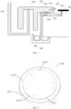
FIG. 2 is a sectional view of a structure of a semiconductor process apparatus according to an embodiment of the present disclosure. -
FIG. 3 is an enlarged view of part of a structure of the semiconductor process apparatus shown inFIG. 2 . -
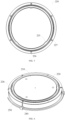
FIG. 4 is a schematic structural diagram of a base of the semiconductor process apparatus shown inFIG. 2 . -
FIG. 5 is a schematic structural diagram of a deposition ring of the semiconductor process apparatus ofFIG. 2 . -
FIG. 6 is a schematic structural diagram of an assembly structure of a base and a deposition ring of the semiconductor process apparatus shown inFIG. 2 . -
FIG. 7 is a schematic structural diagram of a first positioning boss of the deposition ring shown inFIG. 5 . -
FIG. 8 is a schematic structural diagram of a cover ring of the semiconductor process apparatus shown inFIG. 2 . -
FIG. 9 is a schematic structural diagram of a buckle slot of the deposition ring shown inFIG. 5 . -
FIG. 10 is a schematic structural diagram of a buckle of the semiconductor process apparatus shown inFIG. 3 . - The technical solutions of the embodiments of present disclosure are clearly and completely described below with reference to the drawings. Apparently, the embodiments described herein are merely some embodiments of the present disclosure, rather than all embodiments. All other embodiments, which are derived by those of ordinary skill in the art based on the embodiments in the present disclosure without any inventive work, fall within the scope of the present disclosure. The embodiments below and the technical features therein may be combined with each other if no conflict is incurred.
- At present, the technique of making interconnect lines of aluminum and aluminum alloys in a semiconductor manufacturing process is widely applied to a metallization process of chip manufacturing. A common manufacturing process is a magnetron sputtering method, and a typical magnetron sputtering apparatus is shown in
FIG. 1 . The magnetron sputtering apparatus is provided with thereaction chamber 10, thesemiconductor process assembly 20 for performing magnetron sputtering is disposed in the upper portion of thereaction chamber 10, and the bearing device for bearing thewafer 40 is disposed in the lower portion of thereaction chamber 10. The bearing device mainly includes thebase 31, thedeposition ring 32, and thecover ring 33. The bottom surface of thedeposition ring 32 is flat and is directly placed on thebase 31; and the top surface of thedeposition ring 32 is provided with the groove for deposition of a reactant generated during a magnetron sputtering process, so as to protect the surface of thebase 31 against contamination by the reactant. In the existing art, since contact parts of thecover ring 33 and thedeposition ring 32 are relatively close to the groove, after the magnetron sputtering process lasts for a period of time, the contact parts of thecover ring 33 and thedeposition ring 32 adhere to each other as the reactant deposited in the groove increases, such that thedeposition ring 32 is also lifted when thecover ring 33 is lifted, resulting in the falling of thedeposition ring 32. Meanwhile, since the inner diameter of thedeposition ring 32 is generally smaller than the diameter of thewafer 40, the lifteddeposition ring 32 can lift thewafer 40 at the same time, resulting in a wafer transfer failure and chipping of thewafer 40. - In view of the above, there is a need to propose a new solution for the bearing device, so as to solve the problems of the falling of the deposition ring, the wafer transfer failure and the chipping of the wafer which are caused because the existing bearing device is prone to adhesion during the magnetron sputtering process.
- As shown in
FIG. 2 to FIG. 4 , in an embodiment, the present disclosure provides a semiconductor process apparatus, including areaction chamber 100 with enclosed space, abearing device 200, and asemiconductor processing assembly 300, with thebearing device 200 and thesemiconductor processing assembly 300 separately disposed in the enclosed space. Thebearing device 200 may include abase 210, adeposition ring 220, and acover ring 230. Thebase 210 may include afirst surface 2111 and asecond surface 2121, thefirst surface 2111 is configured to bear awafer 400, a height of thesecond surface 2121 is smaller than that of thefirst surface 2111, and thesecond surface 2121 is disposed around thefirst surface 2111. Thedeposition ring 220 may include an upper surface provided with anannular groove 221, and a lower surface covering thesecond surface 2121 for protecting thesecond surface 2121 against contamination by a reactant during a semiconductor processing process on thewafer 400. Thecover ring 230 may be configured to cover a gap between thebase 210 and aliner 110 of thereaction chamber 100 of the semiconductor process apparatus, so as to prevent the reactant from contaminating a lower region of thereaction chamber 100, an outer ring portion of thecover ring 230 is supported on theliner 110 of thereaction chamber 100 of the semiconductor process apparatus, an inner ring portion of thecover ring 230 covers an outer ring portion of thedeposition ring 220, and a plurality of annular protrusions and a plurality of annular recesses are disposed between the inner ring portion of thecover ring 230 and the outer ring portion of thedeposition ring 220, so as to form a labyrinth passage between theannular groove 221 and contact parts of thecover ring 230 and thedeposition ring 220. - It should be noted that the semiconductor process apparatus may be a magnetron sputtering apparatus, in which case the
semiconductor processing assembly 300 is a magnetron sputtering assembly, which may include amagnetron system 310, atarget 320, and an upper electrode system (not shown). Thetarget 320 is located above thebearing device 200, and forms a closed cavity in the upper portion of thereaction chamber 100, and the closed cavity may be filled with deionized water. When a magnetron sputtering process is performed on thewafer 400 on thebearing device 200, a direct current (DC) power supply of the upper electrode system may apply a bias voltage to thetarget 320 to endow thetarget 320 with a negative bias voltage relative to the grounded chamber, so that a process gas such as argon may discharge to generate plasma, and meanwhile positively charged argon ions are attracted to thetarget 320 under the action of the negative bias voltage. When the energy of the argon ions is high enough and the argon ions bombard thetarget 320 under the action of a magnetic field generated by themagnetron system 310, metal atoms are caused to escape from a surface of thetarget 320 and are deposited on thewafer 400 through diffusion, thereby completing the magnetron sputtering process on thewafer 400. It is apparent to those of ordinary skill in the art that the semiconductor process apparatus may be an apparatus for performing other semiconductor processing processes on thewafer 400, in which case thesemiconductor processing assembly 300 may be simply replaced with assemblies capable of performing the corresponding semiconductor processing processes. - As shown in
FIG. 2 andFIG. 3 , a main objective of forming the labyrinth passage between theannular groove 221 and the contact parts of thecover ring 230 and thedeposition ring 220 by providing the plurality of annular protrusions and the plurality of annular recesses between the inner ring portion of thecover ring 230 and the outer ring portion of thedeposition ring 220 in the present embodiment is to increase the difficulty of the reactant deposited in the annular groove in reaching the contact parts, so as to reduce the probability of adhesion of the contact parts. Therefore, the number of the plurality of annular protrusions and the number of the plurality of annular recesses may be set as much as possible according to an actual setting environment. The plurality of annular protrusions are different in height, the plurality of annular recesses are different in depth, and a certain gap is provided between the highest point of an annular protrusion and the lowest point of a corresponding annular recess, so as to better form the labyrinth passage. According to actual needs, the plurality of annular protrusions may be all disposed at an upper surface of the outer ring portion of thedeposition ring 220, or all disposed at a lower surface of the inner ring portion of thecover ring 230, or part of the plurality of annular protrusions may be disposed at the upper surface of the outer ring portion of thedeposition ring 220 and the rest of the plurality of annular protrusions may be disposed at the lower surface of the inner ring portion of thecover ring 230. Similarly, according to actual needs, the plurality of annular recesses may be all disposed at the upper surface of the outer ring portion of thedeposition ring 220, or all disposed at the lower surface of the inner ring portion of thecover ring 230, or part of the plurality of annular recesses may be disposed at the upper surface of the outer ring portion of thedeposition ring 220 and the rest of the plurality of annular recesses may be disposed at the lower surface of the inner ring portion of thecover ring 230. - In order to enable the labyrinth passage to better prevent the reactant deposited in the
annular groove 221 from reaching the contact parts of thecover ring 230 and thedeposition ring 220, an entrance of the labyrinth passage may be located on a top side of an outer sidewall of theannular groove 221, and is located at a horizontal height greater than that of the contact parts of thecover ring 230 and thedeposition ring 220. Preferably, the inner ring portion of the cover ring may have an eave structure covering part of the annular groove. Taking the case illustrated byFIG. 3 as an example, the plurality of annular protrusions may include a firstannular protrusion 222 and a secondannular protrusion 223 which are respectively disposed at the upper surface of the outer ring portion of thedeposition ring 220, and the plurality of annular recesses include a firstannular recess 224 disposed at the upper surface of the outer ring portion of thedeposition ring 220, and a secondannular recess 231, a thirdannular recess 232, and a thirdannular recess 233 which are respectively disposed at the lower surface of the inner ring portion of thecover ring 230. The firstannular protrusion 222 may be formed on the outer sidewall of theannular groove 221, that is, integrally formed with the outer sidewall of theannular groove 221, so as to form a first labyrinth shield against the reactant which is deposited in theannular groove 221 during the semiconductor processing process. A top side (i.e., the highest point) of the firstannular protrusion 222 is spaced apart from a bottom wall (i.e., the lowest point) of the corresponding secondannular recess 231 by a first preset distance, a height of the secondannular protrusion 223 is smaller than that of the firstannular protrusion 222, a top side (i.e., the highest point) of the secondannular protrusion 223 is spaced apart from a bottom wall (i.e., the lowest point) of the corresponding thirdannular recess 232 by a second preset distance, and the thirdannular recess 233 is disposed adjacent to the contact parts, thereby forming the labyrinth passage together. Furthermore, the contact of thecover ring 230 with thedeposition ring 220 is realized in such a way that thecover ring 230 contacts an outermost edge of thedeposition ring 220; and with the thirdannular recess 233 disposed adjacent to the contact parts, the contact of thecover ring 230 with thedeposition ring 220 is realized in such a way that an outer sidewall (which may form a certain protrusion) of the thirdannular recess 233 contacts the outermost edge of thedeposition ring 220, so that a channel with a certain length is formed between a bottom wall (i.e., the lowest point) of the thirdannular recess 233 and the upper surface of the outer ring portion of thedeposition ring 220. In this way, even if the reactant passes across the first labyrinth shield, the reactant needs to pass through the long channel before reaching the contact parts. Thus, a second labyrinth shield is formed. - Thus, due to the labyrinth passage formed between the
annular groove 221 and the contact parts of thecover ring 230 and thedeposition ring 220, a distance for the reactant which is deposited in theannular groove 221 during the semiconductor processing process to reach the contact parts is greatly increased; and meanwhile, the reactant needs to pass across multiple labyrinth shields before reaching the contact parts, so that the difficulty of the reactant in reaching the contact parts is greatly increased. Therefore, the bearing device of the present disclosure can effectively reduce the probability of adhesion between thecover ring 230 and thedeposition ring 220 during the semiconductor processing process. - In some examples, as shown in
FIG. 4 , thebase 210 includes afirst cylinder 211 and asecond cylinder 212. Thefirst cylinder 211 and thesecond cylinder 212 are vertically and concentrically arranged and connected to each other, that is, thefirst cylinder 211 and thesecond cylinder 212 are coaxially arranged and connected to each other, thefirst cylinder 211 is located on thesecond cylinder 212, and a radius of a bottom surface of thefirst cylinder 211 is smaller than that of a bottom surface of thesecond cylinder 212, so as to respectively form thefirst surface 2111 and thesecond surface 2121 on an upper side of thebase 210. In order to better bear thewafer 400 on thefirst surface 2111, a diameter of thefirst surface 2111 may be smaller than that of thewafer 400. Meanwhile, in order to meet the requirements of some semiconductor process apparatuses for heating thewafer 400 during semiconductor processing processes, thebase 210 may be provided therein with some conventional heating structures, so as to perform corresponding heating processes on thebase 210. - In some examples, as shown in
FIG. 4 ,FIG. 5, and FIG. 6 , an inner ring portion of thedeposition ring 220 and an outer sidewall of thefirst cylinder 211 are positioned by engagement of a plurality offirst positioning bosses 225 and a plurality offirst positioning grooves 2112 in a one-to-one correspondence manner. For those of ordinary skill in the art, both the number of thefirst positioning bosses 225 and the number of thefirst positioning grooves 2112 may be arbitrarily reduced according to actual needs as long as it is ensured that the number of thefirst positioning bosses 225 is equal to the number of thefirst positioning grooves 2112. Meanwhile, according to actual needs, the plurality offirst positioning bosses 225 may be all disposed on an inner circumferential side of thedeposition ring 220, or all disposed at the outer sidewall of thefirst cylinder 211, or part of the plurality offirst positioning bosses 225 may be disposed on the inner circumferential side of thedeposition ring 220, and the rest of the plurality offirst positioning bosses 225 may be disposed at the outer sidewall of thefirst cylinder 211. Similarly, according to actual needs, the plurality offirst positioning grooves 2112 may be all disposed on the inner circumferential side of thedeposition ring 220, or all disposed at the outer sidewall of thefirst cylinder 211, or part of the plurality offirst positioning grooves 2112 may be disposed on the inner circumferential side of thedeposition ring 220, and the rest of the plurality offirst positioning grooves 2112 may be disposed at the outer sidewall of thefirst cylinder 211. Taking the case illustrated byFIG. 4 ,FIG. 5, and FIG. 6 as an example, both the number of thefirst positioning bosses 225 and the number of thefirst positioning grooves 2112 may be three. In such case, the threefirst positioning bosses 225 are all disposed on the inner circumferential side of thedeposition ring 220, and are distributed in an equilateral triangle to ensure stability of a final positioning effect. Correspondingly, the threefirst positioning grooves 2112 are all disposed at the outer sidewall of thefirst cylinder 211, and are also correspondingly distributed in an equilateral triangle, so that eachfirst positioning boss 225 may be correspondingly engaged in the correspondingfirst positioning groove 2112. In addition, in order to further ensure firmness of the engagement, eachfirst positioning boss 225 may be a trapezoidal bass shown inFIG. 7 . Correspondingly, eachfirst positioning groove 2112 may be a trapezoidal groove shown inFIG. 4 which fits the trapezoidal boss. - In some examples, in order to ensure that a center of the
cover ring 230 always coincides with a center of thedeposition ring 220 to avoid a shift of a process result, as shown inFIG. 5, FIG. 6 , andFIG. 8 , the inner ring portion of thecover ring 230 and the outer ring portion of thedeposition ring 220 are positioned by engagement of a plurality ofsecond positioning bosses 226 and a plurality ofsecond positioning grooves 234 in a one-to-one correspondence manner. For those of ordinary skill in the art, both the number of thesecond positioning bosses 226 and the number of thesecond positioning grooves 234 may be arbitrarily reduced according to actual needs as long as it is ensured that the number of thesecond positioning bosses 226 is equal to the number of thesecond positioning grooves 234. Meanwhile, according to actual needs, the plurality ofsecond positioning bosses 226 may be all disposed at the upper surface of the outer ring portion of thedeposition ring 220, or all disposed at the lower surface of the inner ring portion of thecover ring 230, or part of the plurality ofsecond positioning bosses 226 may be disposed at the upper surface of the outer ring portion of thedeposition ring 220, and the rest of the plurality ofsecond positioning bosses 226 may be disposed at the lower surface of the inner ring portion of thecover ring 230. Similarly, according to actual needs, the plurality ofsecond positioning grooves 234 may be all disposed at the upper surface of the outer ring portion of thedeposition ring 220, or all disposed at the lower surface of the inner ring portion of thecover ring 230, or part of the plurality ofsecond positioning grooves 234 may be disposed at the upper surface of the outer ring portion of thedeposition ring 220, and the rest of the plurality ofsecond positioning grooves 234 may be disposed at the lower surface of the inner ring portion of thecover ring 230. Taking the case illustrated byFIG. 5, FIG. 6 , andFIG. 8 as an example, both the number of thesecond positioning bosses 226 and the number of thesecond positioning grooves 234 may be three. In such case, the threesecond positioning bosses 226 are all disposed at the upper surface of the outer ring portion of thedeposition ring 220, and are distributed in an equilateral triangle to ensure stability of a final positioning effect. Correspondingly, the threesecond positioning grooves 234 are all disposed at the lower surface of the inner ring portion of thecover ring 230, and are also correspondingly distributed in an equilateral triangle, so that eachsecond positioning boss 226 may be correspondingly engaged in the correspondingsecond positioning groove 234. In addition, in order to further ensure firmness of the engagement, eachsecond positioning boss 226 may be a trapezoidal bass shown inFIG. 6 . Correspondingly, eachsecond positioning groove 234 may be a trapezoidal groove shown inFIG. 4 which fits the trapezoidal boss. - Since the reactant deposited in the
annular groove 221 may be continuously increased after duration of a semiconductor process (which may be a magnetron sputtering process) on thewafer 400 on thebearing device 200 is increased, the possibility of the reactant passing through the labyrinth passage to reach the contact parts of thecover ring 230 and thedeposition ring 220 is increased. In view of this, in some examples, as shown inFIG. 2 ,FIG. 3 , andFIG. 5 , the outer ring portion of thedeposition ring 220 is further provided with a plurality ofbuckle slots 227, the bearing device further includes a plurality ofbuckles 240, the outer ring portion of thedeposition ring 220 is fastened to thebase 210 by engagement of the plurality ofbuckles 240 and the plurality ofbuckle slots 227 in a one-to-one correspondence manner. In this way, thedeposition ring 220 is firmly fastened on thebase 210 by the engagement of the plurality ofbuckles 240 and the plurality ofbuckle slots 227 in a one-to-one correspondence manner, so that even if the contact parts of thecover ring 230 and thedeposition ring 220 adhere to each other, thedeposition ring 220 is not lifted when thecover ring 230 is lifted. It is apparent to those of ordinary skill in the art that the number of thebuckle slots 227 may be arbitrarily reduced according to actual needs. In order to further firmly fasten thedeposition ring 220 on thebase 210, the number of thebuckle slots 227 may be three, and the threebuckle slots 227 are distributed in an equilateral triangle. Meanwhile, as shown inFIG. 3 ,FIG. 9, and FIG. 10 , eachbuckle 240 may include abuckle rod 241, afirst hook 242 is provided at one end of thebuckle rod 241 to be hooked to acorresponding buckle slot 227, and asecond hook 243 is provided at the other end of thebuckle rod 241 to be hooked to a bottom surface of thebase 210. In this way, when eachbuckle 240 is mounted, thefirst hook 242 may be disposed in thecorresponding buckle slot 227, and then thebuckle 240 may be rotated around a top end of thebuckle rod 241 as a center to hook thesecond hook 243 to the bottom surface of thebase 210, thereby completing the installation of thecorresponding buckle 240. In order to further ensure installation firmness of thefirst hook 242 and prevent thefirst hook 242 from falling off from thecorresponding buckle slot 227, thebuckle slot 227 may be a T-shaped slot, and thefirst hook 242 may be a T-shaped hook which fits the T-shaped slot. Meanwhile, each of two ends of a horizontal portion of the T-shaped hook may be provided with a cylindrical head, so as to further enhance the connection of thefirst hook 242 to thecorresponding buckle slot 227. - Finally, with the three
buckles 240, thedeposition ring 220 can be firmly fastened on thebase 210, and the freedom of thedeposition ring 220 to move up and down can be limited. However, the possibility of circumferential movement of thedeposition ring 220 still exists, which may cause thebuckles 240 to fall off. In view of this, in some examples, as shown inFIG. 2 ,FIG. 3 , andFIG. 6 , thebearing device 200 further includes a fixingring 250, which is disposed around an outer sidewall of thebase 210, and fastens the plurality ofbuckles 240 to the outer sidewall of thebase 210. Furthermore, athird hook 244 is provided at the other end of thebuckle rod 241 to be hooked to the fixing ring. In this way, by placing the fixingring 250 in thethird hook 244 of eachbuckle 240, the circumferential freedom of eachbuckle 240 is limited, which can prevent thebuckle 240 from being rotated and falling off. - In an embodiment, the present disclosure further provides a bearing device for a semiconductor process apparatus. A structure and functions of the bearing device may be found in the description of the bearing device provided in the above embodiments, and are not described in detail here.
- Although the present disclosure is described by illustration of one or more implementations, variations and modifications may be envisaged by those of ordinary skill in the art based on reading and understanding of the description and the drawings of the present disclosure. The present disclosure includes all those modifications and variations, and is limited only by the scope of the appended claims. In particular, for each function performed by the aforesaid components, the terms used to describe the components are intended to be corresponding to any component (that is functionally equivalent, for example) which performs the specified function of the described components (unless otherwise indicated), even if the any component has a structure different from the disclosed structure which performs the function in the exemplary implementations illustrated herein.
- That is, what is described above is just the embodiments of the present disclosure, and is not intended to limit the scope of the present disclosure, and all equivalent structures or equivalent flow transformations derived from the contents of the description and the drawings of the present disclosure, such as the combinations of the technical features of the embodiments or direct or indirect applications of the technical features of the embodiments to other related technical fields, are included in the scope of the present disclosure.
- In addition, in the description of the present disclosure, it should be understood that the orientations or positional relationships indicated by the terms "center", "longitudinal", "lateral", "length", "width", "thickness", "above", "below", "front", "back", "left", "right", "vertical", "horizontal", "top", "bottom", "inner", "outer" and the like are the orientations or positional relationships based on the drawings, and those terms are used simply for conveniently describing the present disclosure and simplifying the description, rather than indicating or implying that the device or element referred to must have a particular orientation or must be constructed and operated in a particular orientation, and therefore, those terms should not be considered as limitation to the present disclosure. In addition, the structural elements having the same or similar characteristics can be identified by the same or different reference numerals in the present disclosure. Furthermore, the terms "first" and "second" are used only for the purpose of description, and should not be interpreted as indicating or implying relative importance or implicitly indicating the number of the technical features referred to. Thus, a feature defined by "first" or "second" may explicitly or implicitly include one or more features. In the description of the present disclosure, unless specifically limited otherwise, "a plurality" means two or more.
- In the present disclosure, the word "exemplary" is used to mean "serving as an example, instance, or illustration". Any embodiment described herein as being "exemplary" is not necessarily to be interpreted as being preferred or being advantageous over other embodiments. The above description is provided to enable any person skilled in the art to implement or use the present disclosure. In the above description, various details are listed for the purpose of explanation. It should be understood by those of ordinary skill in the art that the present disclosure may be implemented without using these specific details. In other embodiments, well-known structures and processes are not described in detail, so as to prevent the description of the present disclosure from being obscure due to the unnecessary details. Thus, the present disclosure is not intended to be limited to the embodiments described herein, but falls within the widest scope of the principle and features disclosed herein.
Claims (11)
- A bearing device for a semiconductor process apparatus, comprising:a base, which comprises a first surface and a second surface, the first surface being configured to bear a wafer, a height of the second surface being smaller than a height of the first surface, and the second surface being disposed around the first surface;a deposition ring, which comprises an upper surface provided with an annular groove, and a lower surface covering the second surface; anda cover ring, an outer ring portion of the cover ring being supported on a liner of a reaction chamber of the semiconductor process apparatus, an inner ring portion of the cover ring covering an outer ring portion of the deposition ring, and a plurality of annular protrusions and a plurality of annular recesses being disposed at two opposite surfaces between the inner ring portion of the cover ring and the outer ring portion of the deposition ring, so as to form a labyrinth passage between the annular groove and contact parts of the cover ring and the deposition ring.
- The bearing device of claim 1 wherein the plurality of annular protrusions are different in height, and the plurality of annular recesses are different in depth;the plurality of annular protrusions are all disposed at an upper surface of the outer ring portion of the deposition ring, and the plurality of annular recesses are all disposed at a lower surface of the inner ring portion of the cover ring; orthe plurality of annular protrusions are all disposed at the lower surface of the inner ring portion of the cover ring, and the plurality of annular recesses are all disposed at the upper surface of the outer ring portion of the deposition ring; orpart of the plurality of annular protrusions and part of the plurality of annular recesses are disposed at the upper surface of the outer ring portion of the deposition ring, and the rest of the plurality of annular protrusions and the rest of the plurality of annular recesses are disposed at the lower surface of the inner ring portion of the cover ring.
- The bearing device of claim 1, wherein the inner ring portion of the cover ring has an eave structure, which covers part of the annular groove.
- The bearing device of claim 1, wherein the base comprises a first cylinder and a second cylinder, the first cylinder and the second cylinder are coaxially arranged and connected to each other, the first cylinder is located on the second cylinder, and a radius of a bottom surface of the first cylinder is smaller than a radius of a bottom surface of the second cylinder, so as to respectively form the first surface and the second surface on an upper side of the base; and an inner ring portion of the deposition ring and an outer sidewall of the first cylinder are positioned by engagement of a plurality of first positioning bosses and a plurality of first positioning grooves in a one-to-one correspondence manner.
- The bearing device of claim 1, wherein the inner ring portion of the cover ring and the outer ring portion of the deposition ring are positioned by engagement of a plurality of second positioning bosses and a plurality of second positioning grooves in a one-to-one correspondence manner.
- The bearing device of claim 1, wherein the outer ring portion of the deposition ring is further provided with a plurality of buckle slots, the bearing device further comprises a plurality of buckles, and the outer ring portion of the deposition ring is fastened to the base by engagement of the plurality of buckles and the plurality of buckle slots in a one-to-one correspondence manner.
- The bearing device of claim 6, wherein each of the plurality of buckles comprises a buckle rod, a first hook is provided at one end of the buckle rod to be hooked to a corresponding buckle slot, and a second hook is provided at the other end of the buckle rod to be hooked to a bottom surface of the base.
- The bearing device of claim 7, wherein the buckle slot is a T-shaped slot, and the first hook is a T-shaped hook which fits the T-shaped slot.
- The bearing device of claim 7, further comprising:
a fixing ring, which is disposed around an outer sidewall of the base, and fastens the plurality of buckles to the outer sidewall of the base. - The bearing device of claim 9, wherein a third hook is provided at the other end of the buckle rod to be hooked to the fixing ring.
- A semiconductor process apparatus, comprising the bearing device of any one of claims 1 to 10, a reaction chamber with enclosed space, and a semiconductor processing assembly, wherein the bearing device and the semiconductor processing assembly are disposed in the enclosed space.
Applications Claiming Priority (2)
| Application Number | Priority Date | Filing Date | Title |
|---|---|---|---|
| CN202210738846.XA CN115074690B (en) | 2022-06-24 | 2022-06-24 | Semiconductor process equipment and bearing device thereof |
| PCT/CN2023/099884 WO2023246561A1 (en) | 2022-06-24 | 2023-06-13 | Semiconductor process apparatus and bearing device therefor |
Publications (1)
| Publication Number | Publication Date |
|---|---|
| EP4545678A1 true EP4545678A1 (en) | 2025-04-30 |
Family
ID=83256108
Family Applications (1)
| Application Number | Title | Priority Date | Filing Date |
|---|---|---|---|
| EP23826210.9A Pending EP4545678A1 (en) | 2022-06-24 | 2023-06-13 | Semiconductor process apparatus and bearing device therefor |
Country Status (5)
| Country | Link |
|---|---|
| EP (1) | EP4545678A1 (en) |
| JP (1) | JP7835905B2 (en) |
| CN (1) | CN115074690B (en) |
| TW (1) | TWI859926B (en) |
| WO (1) | WO2023246561A1 (en) |
Families Citing this family (3)
| Publication number | Priority date | Publication date | Assignee | Title |
|---|---|---|---|---|
| CN115074690B (en) * | 2022-06-24 | 2023-10-13 | 北京北方华创微电子装备有限公司 | Semiconductor process equipment and bearing device thereof |
| CN118581442B (en) * | 2023-03-03 | 2025-11-11 | 北京北方华创微电子装备有限公司 | Process chamber and semiconductor process equipment |
| CN119411104A (en) * | 2024-12-13 | 2025-02-11 | 拓荆科技(上海)有限公司 | Process chamber and thin film deposition equipment |
Family Cites Families (17)
| Publication number | Priority date | Publication date | Assignee | Title |
|---|---|---|---|---|
| US6440879B1 (en) * | 2001-01-05 | 2002-08-27 | Integrated Device Technology, Inc. | Physical vapor deposition apparatus with modified shutter disk and cover ring |
| US9127362B2 (en) | 2005-10-31 | 2015-09-08 | Applied Materials, Inc. | Process kit and target for substrate processing chamber |
| US20090050272A1 (en) * | 2007-08-24 | 2009-02-26 | Applied Materials, Inc. | Deposition ring and cover ring to extend process components life and performance for process chambers |
| US8900471B2 (en) | 2009-02-27 | 2014-12-02 | Applied Materials, Inc. | In situ plasma clean for removal of residue from pedestal surface without breaking vacuum |
| WO2012024061A2 (en) | 2010-08-20 | 2012-02-23 | Applied Materials, Inc. | Extended life deposition ring |
| JP6715019B2 (en) | 2016-02-09 | 2020-07-01 | 株式会社Screenホールディングス | Substrate processing apparatus and substrate processing method |
| CN207176067U (en) * | 2017-06-08 | 2018-04-03 | 北京北方华创微电子装备有限公司 | Deposition ring and chuck assembly |
| CN109023287B (en) * | 2017-06-08 | 2024-05-17 | 北京北方华创微电子装备有限公司 | Deposition ring and chuck assembly |
| CN109837518B (en) * | 2017-11-28 | 2021-06-08 | 北京北方华创微电子装备有限公司 | Deposition ring fixing assembly, bearing device and reaction chamber |
| CN208308944U (en) * | 2017-12-29 | 2019-01-01 | 中航(重庆)微电子有限公司 | A kind of sputtering chamber and Pvd equipment |
| CN111254383B (en) * | 2020-03-25 | 2020-09-25 | 上海陛通半导体能源科技股份有限公司 | Physical vapor deposition equipment for improving uniformity of reactive sputtering film |
| CN112030130B (en) * | 2020-08-27 | 2023-06-13 | 上海华力集成电路制造有限公司 | Positioning structure and positioning method thereof |
| CN214193444U (en) * | 2020-11-25 | 2021-09-14 | 鑫天虹(厦门)科技有限公司 | Film deposition equipment for reducing fine dust and shielding component thereof |
| CN214736062U (en) * | 2021-03-25 | 2021-11-16 | 鑫天虹(厦门)科技有限公司 | Substrate bearing and fixing device and thin film deposition equipment |
| CN113322440B (en) * | 2021-05-26 | 2022-08-16 | 北京北方华创微电子装备有限公司 | Semiconductor processing equipment and process chamber thereof |
| TWM620754U (en) * | 2021-08-31 | 2021-12-01 | 天虹科技股份有限公司 | Wafer carrying and fixing device and thin film deposition equipment using the wafer carrying and fixing device |
| CN115074690B (en) * | 2022-06-24 | 2023-10-13 | 北京北方华创微电子装备有限公司 | Semiconductor process equipment and bearing device thereof |
-
2022
- 2022-06-24 CN CN202210738846.XA patent/CN115074690B/en active Active
-
2023
- 2023-06-13 TW TW112122029A patent/TWI859926B/en active
- 2023-06-13 WO PCT/CN2023/099884 patent/WO2023246561A1/en not_active Ceased
- 2023-06-13 JP JP2024574615A patent/JP7835905B2/en active Active
- 2023-06-13 EP EP23826210.9A patent/EP4545678A1/en active Pending
Also Published As
| Publication number | Publication date |
|---|---|
| TWI859926B (en) | 2024-10-21 |
| WO2023246561A1 (en) | 2023-12-28 |
| JP7835905B2 (en) | 2026-03-25 |
| TW202401545A (en) | 2024-01-01 |
| CN115074690B (en) | 2023-10-13 |
| CN115074690A (en) | 2022-09-20 |
| WO2023246561A9 (en) | 2025-01-16 |
| JP2025519804A (en) | 2025-06-26 |
Similar Documents
| Publication | Publication Date | Title |
|---|---|---|
| EP4545678A1 (en) | Semiconductor process apparatus and bearing device therefor | |
| KR102415847B1 (en) | Universal process kit | |
| CN206418192U (en) | Collimater, collimator assembly and substrate processing chamber | |
| US20090308739A1 (en) | Wafer processing deposition shielding components | |
| KR102020010B1 (en) | Wafer processing deposition shielding components | |
| US12344929B2 (en) | Multi-functional shutter disk for thin film deposition chamber | |
| TWI515765B (en) | Method and apparatus for processing substrates using a selectively grounded and movable process collar | |
| US10580622B2 (en) | Plasma processing apparatus | |
| TW201802274A (en) | Non-disappearing anode for use with dielectric deposition | |
| HK40118968A (en) | Semiconductor process apparatus and bearing device therefor | |
| EP0742579A2 (en) | A method and apparatus for concentrating plasma on a substrate surface during processing | |
| EP1700334A1 (en) | Electrostatic chuck and chuck base having cooling path for cooling wafer | |
| EP2368258B1 (en) | Rf sputtering arrangement | |
| US20200024725A1 (en) | Pre-conditioned chamber components | |
| US10072330B2 (en) | Shield mask mounting fitting for a sputtering apparatus | |
| CN109755089B (en) | Plasma cavity and semiconductor processing equipment | |
| KR20210045340A (en) | Sputtering apparatus | |
| KR20010053749A (en) | Ionic Metal Plasma Device |
Legal Events
| Date | Code | Title | Description |
|---|---|---|---|
| STAA | Information on the status of an ep patent application or granted ep patent |
Free format text: STATUS: THE INTERNATIONAL PUBLICATION HAS BEEN MADE |
|
| PUAI | Public reference made under article 153(3) epc to a published international application that has entered the european phase |
Free format text: ORIGINAL CODE: 0009012 |
|
| STAA | Information on the status of an ep patent application or granted ep patent |
Free format text: STATUS: REQUEST FOR EXAMINATION WAS MADE |
|
| 17P | Request for examination filed |
Effective date: 20250103 |
|
| AK | Designated contracting states |
Kind code of ref document: A1 Designated state(s): AL AT BE BG CH CY CZ DE DK EE ES FI FR GB GR HR HU IE IS IT LI LT LU LV MC ME MK MT NL NO PL PT RO RS SE SI SK SM TR |
|
| REG | Reference to a national code |
Ref country code: HK Ref legal event code: DE Ref document number: 40118968 Country of ref document: HK |
|
| DAV | Request for validation of the european patent (deleted) | ||
| DAX | Request for extension of the european patent (deleted) |