EP4539087A1 - Field emission device, and x-ray generation device using same - Google Patents
Field emission device, and x-ray generation device using same Download PDFInfo
- Publication number
- EP4539087A1 EP4539087A1 EP22946958.0A EP22946958A EP4539087A1 EP 4539087 A1 EP4539087 A1 EP 4539087A1 EP 22946958 A EP22946958 A EP 22946958A EP 4539087 A1 EP4539087 A1 EP 4539087A1
- Authority
- EP
- European Patent Office
- Prior art keywords
- field emission
- condition
- emission device
- gate electrode
- layer
- Prior art date
- Legal status (The legal status is an assumption and is not a legal conclusion. Google has not performed a legal analysis and makes no representation as to the accuracy of the status listed.)
- Pending
Links
Images









Classifications
-
- H—ELECTRICITY
- H01—ELECTRIC ELEMENTS
- H01J—ELECTRIC DISCHARGE TUBES OR DISCHARGE LAMPS
- H01J35/00—X-ray tubes
- H01J35/02—Details
- H01J35/04—Electrodes ; Mutual position thereof; Constructional adaptations therefor
- H01J35/06—Cathodes
-
- H—ELECTRICITY
- H01—ELECTRIC ELEMENTS
- H01J—ELECTRIC DISCHARGE TUBES OR DISCHARGE LAMPS
- H01J1/00—Details of electrodes, of magnetic control means, of screens, or of the mounting or spacing thereof, common to two or more basic types of discharge tubes or lamps
- H01J1/02—Main electrodes
- H01J1/30—Cold cathodes, e.g. field-emissive cathode
- H01J1/312—Cold cathodes, e.g. field-emissive cathode having an electric field perpendicular to the surface, e.g. tunnel-effect cathodes of metal-insulator-metal [MIM] type
-
- H—ELECTRICITY
- H01—ELECTRIC ELEMENTS
- H01J—ELECTRIC DISCHARGE TUBES OR DISCHARGE LAMPS
- H01J35/00—X-ray tubes
- H01J35/02—Details
- H01J35/04—Electrodes ; Mutual position thereof; Constructional adaptations therefor
- H01J35/06—Cathodes
- H01J35/065—Field emission, photo emission or secondary emission cathodes
-
- H—ELECTRICITY
- H01—ELECTRIC ELEMENTS
- H01J—ELECTRIC DISCHARGE TUBES OR DISCHARGE LAMPS
- H01J1/00—Details of electrodes, of magnetic control means, of screens, or of the mounting or spacing thereof, common to two or more basic types of discharge tubes or lamps
- H01J1/02—Main electrodes
- H01J1/30—Cold cathodes, e.g. field-emissive cathode
- H01J1/304—Field-emissive cathodes
-
- H—ELECTRICITY
- H01—ELECTRIC ELEMENTS
- H01J—ELECTRIC DISCHARGE TUBES OR DISCHARGE LAMPS
- H01J1/00—Details of electrodes, of magnetic control means, of screens, or of the mounting or spacing thereof, common to two or more basic types of discharge tubes or lamps
- H01J1/02—Main electrodes
- H01J1/30—Cold cathodes, e.g. field-emissive cathode
- H01J1/308—Semiconductor cathodes, e.g. cathodes with PN junction layers
-
- H—ELECTRICITY
- H01—ELECTRIC ELEMENTS
- H01J—ELECTRIC DISCHARGE TUBES OR DISCHARGE LAMPS
- H01J1/00—Details of electrodes, of magnetic control means, of screens, or of the mounting or spacing thereof, common to two or more basic types of discharge tubes or lamps
- H01J1/46—Control electrodes, e.g. grid; Auxiliary electrodes
-
- H—ELECTRICITY
- H01—ELECTRIC ELEMENTS
- H01J—ELECTRIC DISCHARGE TUBES OR DISCHARGE LAMPS
- H01J35/00—X-ray tubes
- H01J35/02—Details
- H01J35/16—Vessels; Containers; Shields associated therewith
- H01J35/18—Windows
-
- H—ELECTRICITY
- H01—ELECTRIC ELEMENTS
- H01J—ELECTRIC DISCHARGE TUBES OR DISCHARGE LAMPS
- H01J2201/00—Electrodes common to discharge tubes
- H01J2201/30—Cold cathodes
- H01J2201/308—Semiconductor cathodes, e.g. having PN junction layers
-
- H—ELECTRICITY
- H01—ELECTRIC ELEMENTS
- H01J—ELECTRIC DISCHARGE TUBES OR DISCHARGE LAMPS
- H01J2201/00—Electrodes common to discharge tubes
- H01J2201/30—Cold cathodes
- H01J2201/312—Cold cathodes having an electric field perpendicular to the surface thereof
- H01J2201/3125—Metal-insulator-Metal [MIM] emission type cathodes
-
- H—ELECTRICITY
- H01—ELECTRIC ELEMENTS
- H01J—ELECTRIC DISCHARGE TUBES OR DISCHARGE LAMPS
- H01J2235/00—X-ray tubes
- H01J2235/06—Cathode assembly
- H01J2235/062—Cold cathodes
-
- H—ELECTRICITY
- H01—ELECTRIC ELEMENTS
- H01J—ELECTRIC DISCHARGE TUBES OR DISCHARGE LAMPS
- H01J2235/00—X-ray tubes
- H01J2235/06—Cathode assembly
- H01J2235/068—Multi-cathode assembly
-
- H—ELECTRICITY
- H01—ELECTRIC ELEMENTS
- H01J—ELECTRIC DISCHARGE TUBES OR DISCHARGE LAMPS
- H01J2235/00—X-ray tubes
- H01J2235/18—Windows, e.g. for X-ray transmission
Definitions
- the present disclosure relates to a field emission device that generates X-rays by emitting an electron beam and an X-ray generating apparatus using the same.
- an X-ray generating apparatus is widely used for medical diagnosis and non-destructive testing to reveal defects inside various structures.
- the X-ray generating apparatus can use field emission devices of various structures as X-ray emission sources.
- X-ray generating apparatus have been using field emission devices with a Metal Insulator Semiconductor (MIS) structure as X-ray emission sources in order to achieve miniaturization and improved resolution.
- MIS Metal Insulator Semiconductor
- the field emission device of the MIS structure includes a semiconductor layer, an insulating layer, and a gate electrode layer, and the field emission performance, reliability, and stability can be determined according to the conditions of the constituent materials, thickness, and structure thereof.
- An object of the present disclosure is to solve the problems described above and the other problems.
- An object of the present disclosure is to provide a field emission device which can improve field emission performance, reliability and stability by forming a semiconductor layer, an insulating layer and a gate electrode layer based on specific conditions, and an X-ray generating apparatus using the same.
- a field emission device includes a semiconductor substrate; a bottom electrode disposed below the semiconductor substrate; an insulating layer disposed above the semiconductor substrate; a gate electrode disposed on the insulating layer; and, a top electrode disposed on the gate electrode; in which the gate electrode may be composed of a material satisfying at least one of a first condition for work function, a second condition for Gibbs free energy of a redox reaction with the insulating layer, a third condition for sublimation energy, and a fourth condition for electron mean free path.
- An X-ray generating apparatus includes a field emission device having a plurality of electron beam emitting regions arranged; and an anode generating X-rays by collision with electrons emitted from the electron beam emission region of the field emission device and reflects and transmits the X-rays in a specific direction
- the field emission device may include a semiconductor substrate; a bottom electrode disposed below the semiconductor substrate; an insulating layer disposed above the semiconductor substrate; a gate electrode disposed on the insulating layer; and, a top electrode disposed on the gate electrode; in which the gate electrode may be composed of a material satisfying at least one of a first condition for work function, a second condition for Gibbs free energy of a redox reaction with the insulating layer, a third condition for sublimation energy, and a fourth condition for electron mean free path.
- a field emission device and an X-ray generating apparatus using the same can improve field emission performance, reliability, and stability by forming a semiconductor layer, an insulating layer, and a gate electrode layer based on specific conditions.
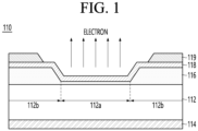
- FIG. 1 is a cross-sectional view illustrating a field emission device according to one embodiment of the present disclosure.
- the field emission device 110 of the present disclosure illustrates, as an example, a field emission device having a MIS (Metal Insulator Semiconductor) structure, and the present disclosure is applicable to field emission devices of various structures, including a field emission device having a MIM (Metal-Insulator-Metal) structure.
- MIS Metal Insulator Semiconductor
- MIM Metal-Insulator-Metal
- the field emission device 110 of the present disclosure may include a semiconductor substrate 112, a bottom electrode 114 disposed below the semiconductor substrate 112, an insulating layer 116 disposed above the semiconductor substrate 112, a gate electrode 118 disposed on the insulating layer 116, and a top electrode 119 disposed on the gate electrode 118.
- the gate electrode 118 may be composed of a material that satisfies at least one of a first condition for the work function, a second condition for the Gibbs free energy of the redox reaction with the insulating layer 116, a third condition for the sublimation energy, and a fourth condition for the electron mean free path.
- the gate electrode 118 may be composed of a material that satisfies one of a first condition in which the work function is about 5.5 eV or less, a second condition in which the Gibbs free energy has a positive value, a third condition in which sublimation energy is about 300 kJ/mol or more, and a fourth condition in which the electron mean free path is about 0.9 nm or more.
- the gate electrode 118 may be composed of a material that satisfies a plurality of conditions among a first condition in which the work function is about 5.5 eV or less, a second condition in which the Gibbs free energy has a positive value, a third condition in which sublimation energy is about 300 kJ/mol or more, and a fourth condition in which the electron mean free path is about 0.9 nm or more.
- the gate electrode 118 may be composed of any one of graphene, metal, and metal compound materials that satisfy a plurality of conditions among a first condition in which the work function is about 5.5 eV or less, a second condition in which the Gibbs free energy has a positive value, a third condition in which sublimation energy is about 300 kJ/mol or more, and a fourth condition in which the electron mean free path is about 0.9 nm or more.
- the gate electrode 118 may be composed of any one of graphene, W, Mo, TiN, Au, Ir, and Pt, but this is only an example and is not limited thereto.
- the gate electrode 118 may be preferentially composed of a material that satisfies a condition with a higher priority among the first to fourth conditions based on preset priorities.
- the preset priorities may be set such that the first condition for the work function is set as the first priority, the second condition for the Gibbs free energy as the second priority, the third condition for sublimation energy as the third priority, and the fourth condition for the electron mean free path as the fourth priority, but this is only an example and is not limited thereto.
- the gate electrode 118 may be preferentially composed of a material that satisfies the highest priority condition among the first to fourth conditions and satisfies the greatest number of conditions.
- the present disclosure proposes conditions of the gate electrode 118 to implement a field emission device with excellent field emission performance and reliability.
- the conditions of the gate electrode 118 may include a first condition for the work function, a second condition for the Gibbs free energy of the redox reaction with the insulating layer 116, a third condition for the sublimation energy, and a fourth condition for the electron mean free path.
- the reason why the work function of the gate electrode 118 is included among the conditions of the gate electrode 118 is as follows.
- the thermal, chemical, and electrical stability of the gate electrode 118 in contact with the insulating layer 116 is a factor related to the reliability of the field emission device 110, and it is important to select the material of the gate electrode 118 so that the phenomenon of the gate electrode 118 diffusing into the insulating layer 116 or reacting with the material of the insulating layer 116 does not occur.
- the reason why the electron mean free path is included among the conditions of the gate electrode 118 is as follows.
- the thickness of the gate electrode 118 may be from about 0.1 nm to about 100 nm.
- the gate electrode 118 can be formed in contact with the insulating layer 116.
- the insulating layer 116 may include at least one of SiO 2 , SiN x , Al 2 O 3 , and Ti 2 O 3 , but this is only an example and is not limited thereto.
- the thickness of the insulating layer 116 may be about 5 nm to about 30 nm.
- the reason why the thickness of the gate electrode 118 and the insulating layer 116 is set to a predetermined range is that if the preset thickness range is exceeded, the field emission performance and reliability may deteriorate.
- the semiconductor substrate 112 may include a plurality of electron beam emitting regions 112a and electron beam non-emitting regions 112b.
- the top electrode 119 can be placed on the gate electrode 118 located in the electron beam non-emitting region 112b.
- the semiconductor substrate 112 is composed of a first conductive type or second conductive type semiconductor, and the first conductive type or second conductive type semiconductor may have a doping concentration in the range of 1 ⁇ 10 14 cm -3 to 1 ⁇ 10 21 cm -3 .
- the semiconductor substrate 112 may be composed of n-type or p-type silicon, and the dopant may include one of boron, phosphorous, and arsenic, but this is only an example and is not limited thereto.
- the semiconductor substrate 112 may include a first semiconductor layer having a first doping concentration and a second semiconductor layer formed on the first semiconductor layer and having a second doping concentration lower than the first doping concentration.
- the first doping concentration of the first semiconductor layer may be 1 ⁇ 10 19 cm -3
- the second doping concentration of the second semiconductor layer may be 1 ⁇ 10 16 cm -3 , but this is only an example and is not limited thereto.
- the thickness of the second semiconductor layer can be thinner than the thickness of the first semiconductor layer.
- the thickness of the semiconductor substrate 112 and the second semiconductor layer may be about 10 nm to about 10 um.
- the second semiconductor layer may be formed as a single layer having a lower surface in contact with the first semiconductor layer and an upper surface in contact with the insulating layer.
- the second semiconductor layer can be formed in both the electron beam emitting region 112a and the electron beam non-emitting region 112b of the semiconductor substrate 112.
- the second semiconductor layer may be partially formed only in the electron beam emitting region 112a of the semiconductor substrate 112.
- the second semiconductor layer is formed to correspond one-to-one to each electron beam emitting region 112a of the semiconductor substrate 112, and the area of one second semiconductor layer may be the area of the corresponding electron beam emitting region 112a or more.
- the area of the second semiconductor layer can be determined so as not to overlap with the top electrode 119 located in the electron beam non-emitting region 112b.
- the second semiconductor layer may be formed of a plurality of doping layers having different doping concentrations, and the doping concentration of the first doping layer in contact with the first semiconductor layer among the doping layers may be higher than the doping concentration of the second doping layer in contact with the insulating layer.
- the second semiconductor layer can be formed in both the electron beam emitting region 112a and the electron beam non-emitting region 112b of the semiconductor substrate 112.
- the second semiconductor layer may be partially formed only in the electron beam emitting region 112a of the semiconductor substrate 112.
- the second semiconductor layer is formed to correspond one-to-one to each electron beam emitting region 112a of the semiconductor substrate 112, and the area of one second semiconductor layer may be greater than the area of the corresponding electron beam emitting region 112a.
- the area of the second semiconductor layer can be determined so as not to overlap with the top electrode 119 located in the electron beam non-emitting region 112b.
- the second semiconductor layer may be formed of a plurality of doping layers having different doping concentrations, and the doping concentration of the doping layers in the plurality of doping layers may gradually increase as they are closer to the first semiconductor layer, and may gradually decrease as they are closer to the insulating layer.
- the reason why the present disclosure forms a doping layer with a low doping concentration in a part or the entire region of the surface of a semiconductor substrate 112 is as follows.
- the quality of the insulating layer of a field emission device is an important factor that determines the performance and stability of the field emission device.
- the insulating layer 116 is composed of silicon dioxide (SiO 2 ) formed by oxidizing silicon which is a semiconductor material, at high temperature, and during the oxidation process, the silicon dopant acts as an impurity and can increase the trap density within the silicon dioxide thin film.
- the present disclosure can obtain a high-quality silicon dioxide thin film without significantly increasing the resistance of the field emission device by forming a doping layer with a low doping concentration on a part or the entire area of the surface of a semiconductor substrate 112, and can secure the performance and reliability of the field emission device.
- top electrode 119 can be electrically connected to the bottom electrode 114 so that a positive voltage can be applied.
- the thickness of the insulating layer 116 positioned in the electron beam emitting region 112a of the semiconductor substrate 112 may be thinner than the thickness of the insulating layer 116 positioned in the electron beam non-emitting region 112b of the semiconductor substrate 112.
- the thickness of the insulating layer 116 can be about 5 nm to about 30 nm.
- the insulating layer 116 may include at least one of SiO 2 , SiN x , Al 2 O 3 , and Ti 2 O 3 , but this is only an example and is not limited thereto.
- the present disclosure can improve field emission performance, reliability and stability by forming a semiconductor layer, an insulating layer and a gate electrode layer based on specific conditions.
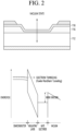
- FIG. 2 is a view illustrating an energy band diagram of a field emission device according to an embodiment of the present disclosure.
- the field emission device of the present disclosure if a certain voltage is applied to the bottom electrode and the top electrode, a strong electric field is induced in a region where the thickness of the insulating layer 116 is thin, and due to this electric field, electrons can tunnel (Fowler-Nordheim) from the semiconductor layer of the semiconductor substrate 112 toward the gate electrode 118 and reach the gate electrode 118.
- a certain voltage is applied to the bottom electrode and the top electrode, a strong electric field is induced in a region where the thickness of the insulating layer 116 is thin, and due to this electric field, electrons can tunnel (Fowler-Nordheim) from the semiconductor layer of the semiconductor substrate 112 toward the gate electrode 118 and reach the gate electrode 118.
- electrons that have energy higher than the work function of the gate electrode 118 can pass through the gate electrode 118 and be emitted into the external space, which is a vacuum state.
- the gate electrode 118 can be a major factor that determines the probability that electrons of the semiconductor will pass through the insulating layer and the gate electrode and be emitted into the vacuum space.
- the present disclosure may configure the gate electrode 118 with a material satisfying at least one of a first condition for a work function, a second condition for a Gibbs free energy of a redox reaction with an insulating layer, a third condition for a heat of sublimation, and a fourth condition for an electron mean free path.
- FIGS. 3 and 4 are graphs illustrating the performance of a field emission device according to the conditions of the gate electrode.
- the present disclosure proposes the following conditions of a gate electrode in order to realize a field emission device having excellent field emission performance and reliability.
- the conditions of the gate electrode may include a first condition for the work function, a second condition for the Gibbs free energy of the redox reaction with the insulating layer, a third condition for sublimation energy, and a fourth condition for the electron mean free path.
- the present disclosure can configure the gate electrode with a material selected from among materials having a work function of about 5.5 eV or less.
- the thermal, chemical, and electrical stability of the gate electrode in contact with the insulating layer can be related to the reliability of the field emission device.
- the gate electrode can easily diffusion when sublimation energy of the gate electrode material is low, and the reaction can easily occur when the Gibbs free energy for redox reaction with the insulating layer material is low (the more negative the value).
- the present disclosure can configure the gate electrode with a material selected from among materials having a Gibbs free energy of a positive value and a heat of sublimation of about 300 kJ/mol or more.
- the electrons In addition, in order for electrons that have passed through the tunnel barrier layer of the insulating layer in the semiconductor substrate and reached the gate electrode to be emitted out of the field emission device through the gate electrode through the tunneling phenomenon, the electrons must minimize their energy loss at the gate electrode.
- the present disclosure can configure the gate electrode with a material selected from materials having an electron mean free path of about 0.9 nm or more.
- FIGS. 5a and 5b are graphs illustrating the performance of a field emission device according to the material of the gate electrode.
- FIG. 5a is a graph illustrating the performance of a field emission device using a Ni/Au metal compound having a work function of about 5.3 as a gate electrode material
- FIG. 5b is a graph illustrating the performance of a field emission device using graphene having a work function of about 4.5 as a gate electrode material.
- performance indicators of a field emission device may include emission efficiency, which is calculated as the ratio of an emission current through which electrons are emitted and a diode current, which represents the electrical performance of a diode.
- the present disclosure was able to increase the emission current density and emission efficiency by applying Ni/Au and graphene materials with low work functions as gate electrode materials.
- the present disclosure can improve the emission current density and emission efficiency by applying a material having a work function of about 5.5 eV or less as a gate electrode material among the conditions of the gate electrode.
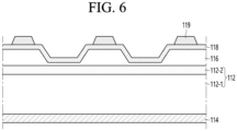
- FIG. 6 is a cross-sectional view illustrating a field emission device according to another embodiment of the present disclosure.
- the field emission device of the present disclosure may include a semiconductor substrate 112, a bottom electrode 114 disposed below the semiconductor substrate 112, an insulating layer 116 disposed above the semiconductor substrate 112, a gate electrode 118 disposed on the insulating layer 116, and a top electrode 119 disposed on the gate electrode 118.
- the semiconductor substrate 112 may include a first semiconductor layer 112-1 having a first doping concentration and a second semiconductor layer 112-2 formed on the first semiconductor layer 112-1 and having a second doping concentration lower than the first doping concentration.
- the first doping concentration of the first semiconductor layer 112-1 may be 1 ⁇ 10 19 cm -3
- the second doping concentration of the second semiconductor layer 112-2 may be 1 ⁇ 10 16 cm -3 , but this is only an example and is not limited thereto.
- the thickness of the second semiconductor layer 112-2 can be thinner than the thickness of the first semiconductor layer 112-1.
- the thickness of the second semiconductor layer 112-2 can be about 10 nm to about 10 um.
- the second semiconductor layer 112-2 can be formed as a single layer with the lower surface contacting the first semiconductor layer 112-1 and the upper surface contacting the insulating layer 116.
- the second semiconductor layer 112-2 can be formed in both the electron beam emitting region 112a and the electron beam non-emitting region 112b of the semiconductor substrate 112.
- the reason why the present disclosure forms a doping layer with a low doping concentration in a part or the entire region of the surface of a semiconductor substrate 112 is as follows.
- the quality of the insulating layer of a field emission device is an important factor that determines the performance and stability of the field emission device.
- the insulating layer 116 is composed of silicon dioxide (SiO 2 ) formed by oxidizing silicon which is a semiconductor material, at high temperature, and thus during the oxidation process, the silicon dopant acts as an impurity and can increase the trap density within the silicon dioxide thin film.
- the present disclosure can obtain a high-quality silicon dioxide thin film without significantly increasing the resistance of the field emission device by forming a doping layer with a low doping concentration on a part or the entire area of the surface of a semiconductor substrate 112, and can secure the performance and reliability of the field emission device.
- FIG. 7 is a graph illustrating electrical characteristics of a field emission device according to another embodiment of the present disclosure.
- the semiconductor substrate of the present disclosure may be configured with a first semiconductor layer in contact with a bottom electrode as a layer having a relatively high doping concentration, and a part or the entire area of a second semiconductor layer in contact with an insulating film as a surface on which an oxidation process is performed may be configured with a layer having a relatively low doping concentration.
- the present disclosure can reduce changes in diode current and emission current over time while minimizing performance degradation of the field emission device due to resistance of the semiconductor substrate, as illustrated in FIG. 7 , thereby ensuring current stability and reliability of the field emission device.
- FIG. 8 is a cross-sectional view illustrating the boundary between semiconductor layers with different doping concentrations
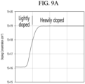
- FIGS. 9a to 9c are graphs illustrating the doping profile of the AB cross section of FIG. 8 .
- the semiconductor substrate 112 of the present disclosure may include a first semiconductor layer 112-1 having a first doping concentration, and a second semiconductor layer 112-2 formed on the first semiconductor layer 112-1 and having a second doping concentration lower than the first doping concentration.
- the doping profile of the interface (A-B cross-section) between the heavily doped first semiconductor layer 112-1 and the lightly doped second semiconductor layer 112-2 may be in a graded or abrupt shape.
- FIGS. 9a to 9c are graphs illustrating the doping profile of the interface between the first semiconductor layer 112-1 and the second semiconductor layer 112-2 when the first doping concentration of the first semiconductor layer 112-1 is about 1 ⁇ 10 19 cm -3 and the second doping concentration of the second semiconductor layer 112-2 is about 1 ⁇ 10 16 cm -3 .
- the doping profile of the interface between the first semiconductor layer 112-1 and the second semiconductor layer 112-2 may have a Gaussian doping profile in a graded shape.
- the doping profile of the boundary between the first semiconductor layer 112-1 and the second semiconductor layer 112-2 may have a linear-graded doping profile in a graded shape.
- the doping profile of the interface between the first semiconductor layer 112-1 and the second semiconductor layer 112-2 may have an abrupt-shaped doping profile.
- FIGS. 10 to 12 are cross-sectional views illustrating a field emission device according to another embodiment of the present disclosure.
- the semiconductor substrate 112 of the present disclosure may include a first semiconductor layer 112-1 having a first doping concentration, and a second semiconductor layer 112-2 formed on the first semiconductor layer 112-1 and having a second doping concentration lower than the first doping concentration.
- the second semiconductor layer 112-2 may be partially formed only in the electron beam emission region 112a of the semiconductor substrate 112.
- the second semiconductor layer 112-2 is formed to correspond one-to-one to each electron beam emitting region 112a of the semiconductor substrate 112, and the area S2 of one second semiconductor layer 112-2 may be greater than or equal to the area S1 of the corresponding electron beam emitting region 112a.
- the area S2 of the second semiconductor layer 112-2 can be determined so as not to overlap with the top electrode 119 located in the electron beam non-emitting region 112b.
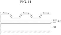
- the second semiconductor layer 112-2 may be formed of a plurality of doping layers 112-2a, 112-2b having different doping concentrations.
- the doping concentration of the first doping layer 112-2a in contact with the first semiconductor layer 112-1 among the doping layers may be higher than the doping concentration of the second doping layer 112-2b in contact with the insulating layer 116.
- the second semiconductor layer 112-2 can be formed in both the electron beam emitting region 112a and the electron beam non-emitting region 112b of the semiconductor substrate 112.
- the second semiconductor layer 112-2 may be partially formed only in the electron beam emitting region 112a of the semiconductor substrate 112.
- the second semiconductor layer 112-2 is formed to correspond one-to-one to each electron beam emitting region 112a of the semiconductor substrate 112, and the area of one second semiconductor layer 112-2 may be greater than or equal to the area of the corresponding electron beam emitting region 112a.
- the area of the second semiconductor layer 112-2 can be determined so as not to overlap with the top electrode 119 located in the electron beam non-emitting region 112b.
- the second semiconductor layer 112-2 is composed of a plurality of doping layers having different doping concentrations, and the doping concentration of the doping layer of the plurality of doping layers may gradually increase as it approaches the first semiconductor layer, and may gradually decrease as it approaches the insulating layer.
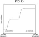
- FIG. 13 is a graph illustrating the doping profile for the field emission devices of FIGS. 11 and 12 .
- the doping profile at the boundary between the doping layers may have an abrupt-shaped doping profile.
- the present disclosure can obtain a high-quality insulating thin film without significantly increasing the resistance of the field emission device by forming a doping layer with a low doping concentration on a part or the entire area of the surface of a semiconductor substrate, and can secure the performance and reliability of the field emission device.
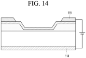
- FIG. 14 is a cross-sectional view illustrating electrical connections of a field emission device according to one embodiment of the present disclosure.
- the top electrode 119 of the present disclosure can be electrically connected to the bottom electrode 114 so that a positive voltage can be applied.
- FIGS. 15 to 17 are cross-sectional views illustrating an X-ray generating apparatus according to an embodiment of the present disclosure.
- the X-ray generating apparatus of the present disclosure may include a field emission device 110 in which a plurality of electron beam emitting regions 112a are arranged, and an anode 120 that generates X-rays by collision with electrons emitted from the electron beam emitting regions 112a of the field emission device 110 and reflects and transmits them in a specific direction.
- the field emission device 110 may include a semiconductor substrate 112, a bottom electrode 114 disposed below the semiconductor substrate 112, an insulating layer 116 disposed above the semiconductor substrate 112, a gate electrode 118 disposed on the insulating layer 116, and a top electrode 119 disposed on the gate electrode 118.
- the gate electrode 118 may be composed of a material that satisfies at least one of the first condition for the work function, the second condition for the Gibbs free energy of the redox reaction with the insulating layer 116, the third condition for the sublimation energy, and the fourth condition for the electron mean free path.
- the gate electrode 118 may be composed of a material that satisfies one of a first condition in which the work function is about 5.5 eV or less, a second condition in which the Gibbs free energy has a positive value, a third condition in which sublimation energy is about 300 kJ/mol or more, and a fourth condition in which the electron mean free path is about 0.9 nm or more.
- the gate electrode 118 may be composed of a material that satisfies a plurality of conditions among a first condition in which the work function is about 5.5 eV or less, a second condition in which the Gibbs free energy has a positive value, a third condition in which sublimation energy is about 300 kJ/mol or more, and a fourth condition in which the electron mean free path is about 0.9 nm or more.
- the gate electrode 118 may be composed of any one of graphene, metal, and metal compound materials that satisfy multiple conditions among a first condition in which the work function is about 5.5 eV or less, a second condition in which the Gibbs free energy has a positive value, a third condition in which sublimation energy is about 300 kJ/mol or more, and a fourth condition in which the electron mean free path is about 0.9 nm or more.
- the semiconductor substrate 112 may include a first semiconductor layer having a first doping concentration and a second semiconductor layer formed on the first semiconductor layer and having a second doping concentration lower than the first doping concentration.
- the anode 120 is disposed at a predetermined interval so as to have a predetermined space from the field emission device 110, and the predetermined space between the anode 120 and the field emission device 110 can be in a vacuum state.
- the anode 120 can be disposed to cover the entire area of the field emission device 110.
- the bottom electrode 114 can be electrically connected in parallel to the top electrode 119 and the anode 120.
- the top electrode 119 can be applied with a first positive voltage
- the anode 120 can be applied with a second positive voltage
- the present disclosure may further include a transmission window 140 disposed over the anode 120 and transmitting X-rays.
- the present disclosure may also dispose the anode 120 to cover only a part of the area of the field emission device 110.
- the anode 120 can be disposed to cover only the electron beam emission regions 112a of the field emission device 110.
- the anode 120 is arranged so that a plurality of sub-anodes are separated and spaced apart at a certain interval, and the sub-anodes can be arranged corresponding to the electron beam emission region 112a of the field emission device 110.
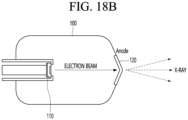
- FIGS. 18a and 18b are views illustrating an X-ray tube to which the field emission device of the present disclosure is applied.
- the present disclosure can be applied to an X-ray tube.
- the reflective X-ray tube of the X-ray generating apparatus 100 is spaced apart at a predetermined interval so that the reflective anode 120 has a predetermined space from the field emission device 110, and the predetermined space between the anode 120 and the field emission device 110 can be in a vacuum state.
- the reflective anode 120 can generate an X-ray by collision with the electrons and reflect it in a specific direction.
- the transmission type X-ray tube of the X-ray generating apparatus 100 is arranged at a predetermined interval so that the reflection type anode 120 has a predetermined space from the field emission device 110, and the predetermined space between the anode 120 and the field emission device 110 can be in a vacuum state.
- the transmission type anode 120 can generate X-rays by collision with electrons and transmit them in a specific direction.
- the field emission device of the present disclosure and the X-ray generating apparatus using the same can improve field emission performance, reliability, and stability by forming a semiconductor layer, an insulating layer, and a gate electrode layer based on specific conditions.
- the field emission performance, reliability and stability can be improved by forming a semiconductor layer, an insulating layer and a gate electrode layer based on specific conditions, and therefore, the industrial applicability is remarkable.
Landscapes
- Cold Cathode And The Manufacture (AREA)
Abstract
Description
- The present disclosure relates to a field emission device that generates X-rays by emitting an electron beam and an X-ray generating apparatus using the same.
- In general, an X-ray generating apparatus is widely used for medical diagnosis and non-destructive testing to reveal defects inside various structures.
- The X-ray generating apparatus can use field emission devices of various structures as X-ray emission sources.
- Recently, X-ray generating apparatus have been using field emission devices with a Metal Insulator Semiconductor (MIS) structure as X-ray emission sources in order to achieve miniaturization and improved resolution.
- The field emission device of the MIS structure includes a semiconductor layer, an insulating layer, and a gate electrode layer, and the field emission performance, reliability, and stability can be determined according to the conditions of the constituent materials, thickness, and structure thereof.
- Therefore, in the future, the development of a field emission device capable of improving field emission performance, reliability, and stability is required, and the development of an X-ray emission device with excellent X-ray generation efficiency and reliability by applying the corresponding field emission device is required.
- An object of the present disclosure is to solve the problems described above and the other problems.
- An object of the present disclosure is to provide a field emission device which can improve field emission performance, reliability and stability by forming a semiconductor layer, an insulating layer and a gate electrode layer based on specific conditions, and an X-ray generating apparatus using the same.
- A field emission device according to one embodiment of the present disclosure includes a semiconductor substrate; a bottom electrode disposed below the semiconductor substrate; an insulating layer disposed above the semiconductor substrate; a gate electrode disposed on the insulating layer; and, a top electrode disposed on the gate electrode; in which the gate electrode may be composed of a material satisfying at least one of a first condition for work function, a second condition for Gibbs free energy of a redox reaction with the insulating layer, a third condition for sublimation energy, and a fourth condition for electron mean free path.
- An X-ray generating apparatus according to one embodiment of the present disclosure includes a field emission device having a plurality of electron beam emitting regions arranged; and an anode generating X-rays by collision with electrons emitted from the electron beam emission region of the field emission device and reflects and transmits the X-rays in a specific direction, in which the field emission device may include a semiconductor substrate; a bottom electrode disposed below the semiconductor substrate; an insulating layer disposed above the semiconductor substrate; a gate electrode disposed on the insulating layer; and, a top electrode disposed on the gate electrode; in which the gate electrode may be composed of a material satisfying at least one of a first condition for work function, a second condition for Gibbs free energy of a redox reaction with the insulating layer, a third condition for sublimation energy, and a fourth condition for electron mean free path.
- According to one embodiment of the present disclosure, a field emission device and an X-ray generating apparatus using the same can improve field emission performance, reliability, and stability by forming a semiconductor layer, an insulating layer, and a gate electrode layer based on specific conditions.
-
-
FIG. 1 is a cross-sectional view illustrating a field emission device according to one embodiment of the present disclosure. -
FIG. 2 is a view illustrating an energy band diagram of a field emission device according to an embodiment of the present disclosure. -
FIGS. 3 and4 are graphs illustrating the performance of a field emission device according to the conditions of the gate electrode. -
FIGS. 5a and5b are graphs illustrating the performance of a field emission device according to the material of the gate electrode. -
FIG. 6 is a cross-sectional view illustrating a field emission device according to another embodiment of the present disclosure. -
FIG. 7 is a graph illustrating electrical characteristics of a field emission device according to another embodiment of the present disclosure. -
FIG. 8 is a cross-sectional view illustrating the boundary between semiconductor layers with different doping concentrations. -
FIGS. 9a to 9c are graphs illustrating the doping profile of the AB cross section ofFIG. 8 . -
FIGS. 10 to 12 are cross-sectional views illustrating a field emission device according to another embodiment of the present disclosure. -
FIG. 13 is a graph illustrating the doping profile for the field emission devices ofFIGS. 11 and12 . -
FIG. 14 is a cross-sectional view illustrating electrical connections of a field emission device according to one embodiment of the present disclosure. -
FIGS. 15 to 17 are cross-sectional views illustrating an X-ray generating apparatus according to an embodiment of the present disclosure. -
FIGS. 18a and18b are views illustrating an X-ray tube to which the field emission device of the present disclosure is applied. - Hereinafter, embodiments disclosed in this specification will be described in detail with reference to the attached drawings, wherein. regardless of the drawing symbols, identical or similar components will be given the same reference numerals and redundant descriptions thereof will be omitted. The suffixes "module" and "part" used for components in the following description are assigned or used interchangeably only for the convenience of writing the specification, and do not have distinct meanings or roles in themselves. In addition, when describing embodiments disclosed in this specification, if it is determined that a specific description of a related known technology may obscure the gist of the embodiments disclosed in this specification, the detailed description thereof will be omitted. In addition, the attached drawings are only intended to facilitate easy understanding of the embodiments disclosed in this specification, and the technical ideas disclosed in this specification are not limited by the attached drawings, and should be understood to include all modifications, equivalents, and substitutes included in the idea and technical scope of the present disclosure.
- Terms including ordinal numbers, such as first, second, and the like, may be used to describe various components, but the components are not limited by the terms. The terms are used only to distinguish one component from another.
- When it is said that a component is "connected" or "accessed" to another component, it should be understood that it may be directly connected or accessed to that other component, but that there may be other components in between. On the other hand, when it is said that a component is "directly connected" or "directly accessed" to another component, it should be understood that there are no other components in between.
-
FIG. 1 is a cross-sectional view illustrating a field emission device according to one embodiment of the present disclosure. - As illustrated in
FIG. 1 , thefield emission device 110 of the present disclosure illustrates, as an example, a field emission device having a MIS (Metal Insulator Semiconductor) structure, and the present disclosure is applicable to field emission devices of various structures, including a field emission device having a MIM (Metal-Insulator-Metal) structure. - The
field emission device 110 of the present disclosure may include asemiconductor substrate 112, abottom electrode 114 disposed below thesemiconductor substrate 112, aninsulating layer 116 disposed above thesemiconductor substrate 112, agate electrode 118 disposed on theinsulating layer 116, and atop electrode 119 disposed on thegate electrode 118. - Here, the
gate electrode 118 may be composed of a material that satisfies at least one of a first condition for the work function, a second condition for the Gibbs free energy of the redox reaction with theinsulating layer 116, a third condition for the sublimation energy, and a fourth condition for the electron mean free path. - For example, the
gate electrode 118 may be composed of a material that satisfies one of a first condition in which the work function is about 5.5 eV or less, a second condition in which the Gibbs free energy has a positive value, a third condition in which sublimation energy is about 300 kJ/mol or more, and a fourth condition in which the electron mean free path is about 0.9 nm or more. - As another example, the
gate electrode 118 may be composed of a material that satisfies a plurality of conditions among a first condition in which the work function is about 5.5 eV or less, a second condition in which the Gibbs free energy has a positive value, a third condition in which sublimation energy is about 300 kJ/mol or more, and a fourth condition in which the electron mean free path is about 0.9 nm or more. - As another example, the
gate electrode 118 may be composed of any one of graphene, metal, and metal compound materials that satisfy a plurality of conditions among a first condition in which the work function is about 5.5 eV or less, a second condition in which the Gibbs free energy has a positive value, a third condition in which sublimation energy is about 300 kJ/mol or more, and a fourth condition in which the electron mean free path is about 0.9 nm or more. - For example, the
gate electrode 118 may be composed of any one of graphene, W, Mo, TiN, Au, Ir, and Pt, but this is only an example and is not limited thereto. - In some cases, the
gate electrode 118 may be preferentially composed of a material that satisfies a condition with a higher priority among the first to fourth conditions based on preset priorities. - As an example, the preset priorities may be set such that the first condition for the work function is set as the first priority, the second condition for the Gibbs free energy as the second priority, the third condition for sublimation energy as the third priority, and the fourth condition for the electron mean free path as the fourth priority, but this is only an example and is not limited thereto.
- In another case, the
gate electrode 118 may be preferentially composed of a material that satisfies the highest priority condition among the first to fourth conditions and satisfies the greatest number of conditions. - In this way, the present disclosure proposes conditions of the
gate electrode 118 to implement a field emission device with excellent field emission performance and reliability. - In other words, the conditions of the
gate electrode 118 may include a first condition for the work function, a second condition for the Gibbs free energy of the redox reaction with theinsulating layer 116, a third condition for the sublimation energy, and a fourth condition for the electron mean free path. - The reason why the work function of the
gate electrode 118 is included among the conditions of thegate electrode 118 is as follows. - This is because, in the
field emission device 110, if voltage is applied to thebottom electrode 114 and thetop electrode 119, a strong electric field is induced in a thin area (tunnel barrier layer) of theinsulating layer 116, and electron tunneling begins, and thus as the work function of thegate electrode 118 decreases, the electric field of the tunnel barrier layer increases, which increases the tunneling current, thereby increasing the field emission performance of thefield emission device 110. - In addition, the reason why the Gibbs free energy of the redox reaction is included among the conditions of the
gate electrode 118 is as follows. - This is because, the thermal, chemical, and electrical stability of the
gate electrode 118 in contact with the insulating layer 116 (particularly, the tunnel barrier layer) is a factor related to the reliability of thefield emission device 110, and it is important to select the material of thegate electrode 118 so that the phenomenon of thegate electrode 118 diffusing into theinsulating layer 116 or reacting with the material of theinsulating layer 116 does not occur. - In addition, the reason why sublimation energy is included among the conditions of the
gate electrode 118 is as follows. - This is because, the
gate electrode 118 diffusion occurs more easily as sublimation energy of the gate electrode material is lower, and the reaction occurs more easily as the Gibbs free energy for the redox reaction with theinsulating layer 116 material is lower (the more negative the value). - In addition, the reason why the electron mean free path is included among the conditions of the
gate electrode 118 is as follows. - This is because, in order for electrons that have passed through the tunnel barrier layer of the
insulating layer 116 in thesemiconductor substrate 112 and reached thegate electrode 118 to be emitted out of thefield emission device 110 through thegate electrode 118 through the tunneling phenomenon, the electrons must minimize their energy loss at thegate electrode 118. - If electrons lose energy due to scattering at the
gate electrode 118 and have energy lower than the work function of thegate electrode 118, they are not emitted out of thefield emission device 110, and thus scattering of the electron at thegate electrode 118 must be minimized, and therefore, the mean free path of electrons in the gate electrode material must be long. - Meanwhile, the thickness of the
gate electrode 118 may be from about 0.1 nm to about 100 nm. - Additionally, the
gate electrode 118 can be formed in contact with the insulatinglayer 116. - For example, the insulating
layer 116 may include at least one of SiO2, SiNx, Al2O3, and Ti2O3, but this is only an example and is not limited thereto. - Additionally, the thickness of the insulating
layer 116 may be about 5 nm to about 30 nm. - Here, the reason why the thickness of the
gate electrode 118 and the insulatinglayer 116 is set to a predetermined range is that if the preset thickness range is exceeded, the field emission performance and reliability may deteriorate. - In addition, the
semiconductor substrate 112 may include a plurality of electronbeam emitting regions 112a and electron beamnon-emitting regions 112b. - Next, the
top electrode 119 can be placed on thegate electrode 118 located in the electron beamnon-emitting region 112b. - Next, the
semiconductor substrate 112 is composed of a first conductive type or second conductive type semiconductor, and the first conductive type or second conductive type semiconductor may have a doping concentration in the range of 1 × 1014 cm-3 to 1 × 1021 cm-3. - For example, the
semiconductor substrate 112 may be composed of n-type or p-type silicon, and the dopant may include one of boron, phosphorous, and arsenic, but this is only an example and is not limited thereto. - Additionally, the
semiconductor substrate 112 may include a first semiconductor layer having a first doping concentration and a second semiconductor layer formed on the first semiconductor layer and having a second doping concentration lower than the first doping concentration. - For example, the first doping concentration of the first semiconductor layer may be 1 × 1019 cm-3, and the second doping concentration of the second semiconductor layer may be 1 × 1016 cm-3, but this is only an example and is not limited thereto.
- In addition, the thickness of the second semiconductor layer can be thinner than the thickness of the first semiconductor layer.
- Here, the thickness of the
semiconductor substrate 112 and the second semiconductor layer may be about 10 nm to about 10 um. - As an example, the second semiconductor layer may be formed as a single layer having a lower surface in contact with the first semiconductor layer and an upper surface in contact with the insulating layer.
- Here, the second semiconductor layer can be formed in both the electron
beam emitting region 112a and the electron beamnon-emitting region 112b of thesemiconductor substrate 112. - In some cases, the second semiconductor layer may be partially formed only in the electron
beam emitting region 112a of thesemiconductor substrate 112. - Here, the second semiconductor layer is formed to correspond one-to-one to each electron
beam emitting region 112a of thesemiconductor substrate 112, and the area of one second semiconductor layer may be the area of the corresponding electronbeam emitting region 112a or more. - At this time, the area of the second semiconductor layer can be determined so as not to overlap with the
top electrode 119 located in the electron beamnon-emitting region 112b. - As another embodiment, the second semiconductor layer may be formed of a plurality of doping layers having different doping concentrations, and the doping concentration of the first doping layer in contact with the first semiconductor layer among the doping layers may be higher than the doping concentration of the second doping layer in contact with the insulating layer.
- Here, the second semiconductor layer can be formed in both the electron
beam emitting region 112a and the electron beamnon-emitting region 112b of thesemiconductor substrate 112. - In some cases, the second semiconductor layer may be partially formed only in the electron
beam emitting region 112a of thesemiconductor substrate 112. - Here, the second semiconductor layer is formed to correspond one-to-one to each electron
beam emitting region 112a of thesemiconductor substrate 112, and the area of one second semiconductor layer may be greater than the area of the corresponding electronbeam emitting region 112a. - At this time, the area of the second semiconductor layer can be determined so as not to overlap with the
top electrode 119 located in the electron beamnon-emitting region 112b. - As another embodiment, the second semiconductor layer may be formed of a plurality of doping layers having different doping concentrations, and the doping concentration of the doping layers in the plurality of doping layers may gradually increase as they are closer to the first semiconductor layer, and may gradually decrease as they are closer to the insulating layer.
- Thus, the reason why the present disclosure forms a doping layer with a low doping concentration in a part or the entire region of the surface of a
semiconductor substrate 112 is as follows. - The quality of the insulating layer of a field emission device is an important factor that determines the performance and stability of the field emission device.
- The insulating
layer 116 is composed of silicon dioxide (SiO2) formed by oxidizing silicon which is a semiconductor material, at high temperature, and during the oxidation process, the silicon dopant acts as an impurity and can increase the trap density within the silicon dioxide thin film. - If using a silicon substrate with a high doping concentration to minimize the resistance of the field emission device, the higher the doping concentration, the lower the resistance, but the thin film quality of the silicon dioxide insulating layer inevitably deteriorates.
- Therefore, the present disclosure can obtain a high-quality silicon dioxide thin film without significantly increasing the resistance of the field emission device by forming a doping layer with a low doping concentration on a part or the entire area of the surface of a
semiconductor substrate 112, and can secure the performance and reliability of the field emission device. - Additionally, the
top electrode 119 can be electrically connected to thebottom electrode 114 so that a positive voltage can be applied. - Next, the thickness of the insulating
layer 116 positioned in the electronbeam emitting region 112a of thesemiconductor substrate 112 may be thinner than the thickness of the insulatinglayer 116 positioned in the electron beamnon-emitting region 112b of thesemiconductor substrate 112. - Here, the thickness of the insulating
layer 116 can be about 5 nm to about 30 nm. - In addition, the insulating
layer 116 may include at least one of SiO2, SiNx, Al2O3, and Ti2O3, but this is only an example and is not limited thereto. - In this way, the present disclosure can improve field emission performance, reliability and stability by forming a semiconductor layer, an insulating layer and a gate electrode layer based on specific conditions.
-
FIG. 2 is a view illustrating an energy band diagram of a field emission device according to an embodiment of the present disclosure. - As illustrated in
FIG. 2 , in the field emission device of the present disclosure, if a certain voltage is applied to the bottom electrode and the top electrode, a strong electric field is induced in a region where the thickness of the insulatinglayer 116 is thin, and due to this electric field, electrons can tunnel (Fowler-Nordheim) from the semiconductor layer of thesemiconductor substrate 112 toward thegate electrode 118 and reach thegate electrode 118. - Among the electrons that reach the
gate electrode 118, electrons that have energy higher than the work function of thegate electrode 118 can pass through thegate electrode 118 and be emitted into the external space, which is a vacuum state. - Here, the
gate electrode 118 can be a major factor that determines the probability that electrons of the semiconductor will pass through the insulating layer and the gate electrode and be emitted into the vacuum space. - Accordingly, the present disclosure may configure the
gate electrode 118 with a material satisfying at least one of a first condition for a work function, a second condition for a Gibbs free energy of a redox reaction with an insulating layer, a third condition for a heat of sublimation, and a fourth condition for an electron mean free path. -
FIGS. 3 and4 are graphs illustrating the performance of a field emission device according to the conditions of the gate electrode. - The present disclosure proposes the following conditions of a gate electrode in order to realize a field emission device having excellent field emission performance and reliability.
- The conditions of the gate electrode may include a first condition for the work function, a second condition for the Gibbs free energy of the redox reaction with the insulating layer, a third condition for sublimation energy, and a fourth condition for the electron mean free path.
- As illustrated in
FIG. 3 , when voltage is applied to the bottom electrode and the top electrode, a strong electric field is induced in a thin area of the insulating layer (tunnel barrier layer) in the field emission device, and electron tunneling begins, and thus as the work function of the gate electrode decreases, the electric field of the tunnel barrier layer increases, which increases the tunneling current, thereby increasing the field emission performance of the field emission device. - Accordingly, the present disclosure can configure the gate electrode with a material selected from among materials having a work function of about 5.5 eV or less.
- In addition, as illustrated in
FIG. 4 , the thermal, chemical, and electrical stability of the gate electrode in contact with the insulating layer (particularly, the tunnel barrier layer) can be related to the reliability of the field emission device. - Therefore, it is important to select the material of the gate electrode so that the phenomenon of the gate electrode diffusing into the insulating layer or reacting with the insulating layer material does not occur.
- The gate electrode can easily diffusion when sublimation energy of the gate electrode material is low, and the reaction can easily occur when the Gibbs free energy for redox reaction with the insulating layer material is low (the more negative the value).
- Accordingly, the present disclosure can configure the gate electrode with a material selected from among materials having a Gibbs free energy of a positive value and a heat of sublimation of about 300 kJ/mol or more.
- In addition, in order for electrons that have passed through the tunnel barrier layer of the insulating layer in the semiconductor substrate and reached the gate electrode to be emitted out of the field emission device through the gate electrode through the tunneling phenomenon, the electrons must minimize their energy loss at the gate electrode.
- If electrons lose energy due to scattering at the gate electrode and have energy lower than the work function of the gate electrode, they will not be emitted out of the field emission device, and thus, scattering at the gate electrode must be minimized, and the mean free path of electrons in the gate electrode material must be long.
- Accordingly, the present disclosure can configure the gate electrode with a material selected from materials having an electron mean free path of about 0.9 nm or more.
-
FIGS. 5a and5b are graphs illustrating the performance of a field emission device according to the material of the gate electrode. -
FIG. 5a is a graph illustrating the performance of a field emission device using a Ni/Au metal compound having a work function of about 5.3 as a gate electrode material, andFIG. 5b is a graph illustrating the performance of a field emission device using graphene having a work function of about 4.5 as a gate electrode material. - As illustrated in
FIGS. 5a and5b , performance indicators of a field emission device may include emission efficiency, which is calculated as the ratio of an emission current through which electrons are emitted and a diode current, which represents the electrical performance of a diode. - Therefore, the present disclosure was able to increase the emission current density and emission efficiency by applying Ni/Au and graphene materials with low work functions as gate electrode materials.
- In other words, the present disclosure can improve the emission current density and emission efficiency by applying a material having a work function of about 5.5 eV or less as a gate electrode material among the conditions of the gate electrode.
-
FIG. 6 is a cross-sectional view illustrating a field emission device according to another embodiment of the present disclosure. - As illustrated in
FIG. 6 , the field emission device of the present disclosure may include asemiconductor substrate 112, abottom electrode 114 disposed below thesemiconductor substrate 112, an insulatinglayer 116 disposed above thesemiconductor substrate 112, agate electrode 118 disposed on the insulatinglayer 116, and atop electrode 119 disposed on thegate electrode 118. - Here, the
semiconductor substrate 112 may include a first semiconductor layer 112-1 having a first doping concentration and a second semiconductor layer 112-2 formed on the first semiconductor layer 112-1 and having a second doping concentration lower than the first doping concentration. - For example, the first doping concentration of the first semiconductor layer 112-1 may be 1 × 1019 cm-3, and the second doping concentration of the second semiconductor layer 112-2 may be 1 × 1016 cm-3, but this is only an example and is not limited thereto.
- In addition, the thickness of the second semiconductor layer 112-2 can be thinner than the thickness of the first semiconductor layer 112-1.
- Here, the thickness of the second semiconductor layer 112-2 can be about 10 nm to about 10 um.
- In this way, the second semiconductor layer 112-2 can be formed as a single layer with the lower surface contacting the first semiconductor layer 112-1 and the upper surface contacting the insulating
layer 116. - Here, the second semiconductor layer 112-2 can be formed in both the electron
beam emitting region 112a and the electron beamnon-emitting region 112b of thesemiconductor substrate 112. - Thus, the reason why the present disclosure forms a doping layer with a low doping concentration in a part or the entire region of the surface of a
semiconductor substrate 112 is as follows. - The quality of the insulating layer of a field emission device is an important factor that determines the performance and stability of the field emission device.
- The insulating
layer 116 is composed of silicon dioxide (SiO2) formed by oxidizing silicon which is a semiconductor material, at high temperature, and thus during the oxidation process, the silicon dopant acts as an impurity and can increase the trap density within the silicon dioxide thin film. - If using a silicon substrate with a high doping concentration to minimize the resistance of the field emission device, the higher the doping concentration, the lower the resistance, but the thin film quality of the silicon dioxide insulating layer inevitably deteriorates.
- Therefore, the present disclosure can obtain a high-quality silicon dioxide thin film without significantly increasing the resistance of the field emission device by forming a doping layer with a low doping concentration on a part or the entire area of the surface of a
semiconductor substrate 112, and can secure the performance and reliability of the field emission device. -
FIG. 7 is a graph illustrating electrical characteristics of a field emission device according to another embodiment of the present disclosure. - The semiconductor substrate of the present disclosure may be configured with a first semiconductor layer in contact with a bottom electrode as a layer having a relatively high doping concentration, and a part or the entire area of a second semiconductor layer in contact with an insulating film as a surface on which an oxidation process is performed may be configured with a layer having a relatively low doping concentration.
- Through this, the present disclosure can reduce changes in diode current and emission current over time while minimizing performance degradation of the field emission device due to resistance of the semiconductor substrate, as illustrated in
FIG. 7 , thereby ensuring current stability and reliability of the field emission device. -
FIG. 8 is a cross-sectional view illustrating the boundary between semiconductor layers with different doping concentrations, andFIGS. 9a to 9c are graphs illustrating the doping profile of the AB cross section ofFIG. 8 . - As illustrated in
FIG. 8 , thesemiconductor substrate 112 of the present disclosure may include a first semiconductor layer 112-1 having a first doping concentration, and a second semiconductor layer 112-2 formed on the first semiconductor layer 112-1 and having a second doping concentration lower than the first doping concentration. - As illustrated in
FIGS. 9a to 9c , the doping profile of the interface (A-B cross-section) between the heavily doped first semiconductor layer 112-1 and the lightly doped second semiconductor layer 112-2 may be in a graded or abrupt shape. -
FIGS. 9a to 9c are graphs illustrating the doping profile of the interface between the first semiconductor layer 112-1 and the second semiconductor layer 112-2 when the first doping concentration of the first semiconductor layer 112-1 is about 1 × 1019cm-3 and the second doping concentration of the second semiconductor layer 112-2 is about 1 × 1016cm-3. - As illustrated in
FIG. 9a , the doping profile of the interface between the first semiconductor layer 112-1 and the second semiconductor layer 112-2 may have a Gaussian doping profile in a graded shape. - In some cases, as illustrated in
FIG. 9b , the doping profile of the boundary between the first semiconductor layer 112-1 and the second semiconductor layer 112-2 may have a linear-graded doping profile in a graded shape. - In another case, as illustrated in
FIG. 9C , the doping profile of the interface between the first semiconductor layer 112-1 and the second semiconductor layer 112-2 may have an abrupt-shaped doping profile. -
FIGS. 10 to 12 are cross-sectional views illustrating a field emission device according to another embodiment of the present disclosure. - As illustrated in
FIG. 10 , thesemiconductor substrate 112 of the present disclosure may include a first semiconductor layer 112-1 having a first doping concentration, and a second semiconductor layer 112-2 formed on the first semiconductor layer 112-1 and having a second doping concentration lower than the first doping concentration. - Here, the second semiconductor layer 112-2 may be partially formed only in the electron
beam emission region 112a of thesemiconductor substrate 112. - Here, the second semiconductor layer 112-2 is formed to correspond one-to-one to each electron
beam emitting region 112a of thesemiconductor substrate 112, and the area S2 of one second semiconductor layer 112-2 may be greater than or equal to the area S1 of the corresponding electronbeam emitting region 112a. - At this time, the area S2 of the second semiconductor layer 112-2 can be determined so as not to overlap with the
top electrode 119 located in the electron beamnon-emitting region 112b. - As another embodiment, as illustrated in
FIG. 11 , the second semiconductor layer 112-2 may be formed of a plurality of doping layers 112-2a, 112-2b having different doping concentrations. - Here, the doping concentration of the first doping layer 112-2a in contact with the first semiconductor layer 112-1 among the doping layers may be higher than the doping concentration of the second doping layer 112-2b in contact with the insulating
layer 116. - Here, the second semiconductor layer 112-2 can be formed in both the electron
beam emitting region 112a and the electron beamnon-emitting region 112b of thesemiconductor substrate 112. - In some cases, as illustrated in
FIG. 12 , the second semiconductor layer 112-2 may be partially formed only in the electronbeam emitting region 112a of thesemiconductor substrate 112. - Here, the second semiconductor layer 112-2 is formed to correspond one-to-one to each electron
beam emitting region 112a of thesemiconductor substrate 112, and the area of one second semiconductor layer 112-2 may be greater than or equal to the area of the corresponding electronbeam emitting region 112a. - At this time, the area of the second semiconductor layer 112-2 can be determined so as not to overlap with the
top electrode 119 located in the electron beamnon-emitting region 112b. - In another case, the second semiconductor layer 112-2 is composed of a plurality of doping layers having different doping concentrations, and the doping concentration of the doping layer of the plurality of doping layers may gradually increase as it approaches the first semiconductor layer, and may gradually decrease as it approaches the insulating layer.
-
FIG. 13 is a graph illustrating the doping profile for the field emission devices ofFIGS. 11 and12 . - As illustrated in
FIG. 13 , if the second semiconductor layer is formed of a plurality of doping layers having different doping concentrations, the doping profile at the boundary between the doping layers may have an abrupt-shaped doping profile. - In this way, the present disclosure can obtain a high-quality insulating thin film without significantly increasing the resistance of the field emission device by forming a doping layer with a low doping concentration on a part or the entire area of the surface of a semiconductor substrate, and can secure the performance and reliability of the field emission device.
-
FIG. 14 is a cross-sectional view illustrating electrical connections of a field emission device according to one embodiment of the present disclosure. - As illustrated in
FIG. 14 , thetop electrode 119 of the present disclosure can be electrically connected to thebottom electrode 114 so that a positive voltage can be applied. - In other words, in the present disclosure, after a positive voltage is applied to the
top electrode 119 and a negative voltage is applied to thebottom electrode 114, if the threshold voltage is exceeded, electron tunneling may occur in the tunnel barrier layer of the field emission device and field emission may begin. -
FIGS. 15 to 17 are cross-sectional views illustrating an X-ray generating apparatus according to an embodiment of the present disclosure. - As illustrated in
FIG. 15 , the X-ray generating apparatus of the present disclosure may include afield emission device 110 in which a plurality of electronbeam emitting regions 112a are arranged, and ananode 120 that generates X-rays by collision with electrons emitted from the electronbeam emitting regions 112a of thefield emission device 110 and reflects and transmits them in a specific direction. - Here, the
field emission device 110 may include asemiconductor substrate 112, abottom electrode 114 disposed below thesemiconductor substrate 112, an insulatinglayer 116 disposed above thesemiconductor substrate 112, agate electrode 118 disposed on the insulatinglayer 116, and atop electrode 119 disposed on thegate electrode 118. - Here, the
gate electrode 118 may be composed of a material that satisfies at least one of the first condition for the work function, the second condition for the Gibbs free energy of the redox reaction with the insulatinglayer 116, the third condition for the sublimation energy, and the fourth condition for the electron mean free path. - For example, the
gate electrode 118 may be composed of a material that satisfies one of a first condition in which the work function is about 5.5 eV or less, a second condition in which the Gibbs free energy has a positive value, a third condition in which sublimation energy is about 300 kJ/mol or more, and a fourth condition in which the electron mean free path is about 0.9 nm or more. - As another example, the
gate electrode 118 may be composed of a material that satisfies a plurality of conditions among a first condition in which the work function is about 5.5 eV or less, a second condition in which the Gibbs free energy has a positive value, a third condition in which sublimation energy is about 300 kJ/mol or more, and a fourth condition in which the electron mean free path is about 0.9 nm or more. - As another example, the
gate electrode 118 may be composed of any one of graphene, metal, and metal compound materials that satisfy multiple conditions among a first condition in which the work function is about 5.5 eV or less, a second condition in which the Gibbs free energy has a positive value, a third condition in which sublimation energy is about 300 kJ/mol or more, and a fourth condition in which the electron mean free path is about 0.9 nm or more. - Additionally, the
semiconductor substrate 112 may include a first semiconductor layer having a first doping concentration and a second semiconductor layer formed on the first semiconductor layer and having a second doping concentration lower than the first doping concentration. - In addition, the
anode 120 is disposed at a predetermined interval so as to have a predetermined space from thefield emission device 110, and the predetermined space between theanode 120 and thefield emission device 110 can be in a vacuum state. - Here, the
anode 120 can be disposed to cover the entire area of thefield emission device 110. - Additionally, the
bottom electrode 114 can be electrically connected in parallel to thetop electrode 119 and theanode 120. - Here, the
top electrode 119 can be applied with a first positive voltage, and theanode 120 can be applied with a second positive voltage. - As another embodiment, as illustrated in
FIG. 16 , the present disclosure may further include atransmission window 140 disposed over theanode 120 and transmitting X-rays. - As another embodiment, as illustrated in
FIG. 17 , the present disclosure may also dispose theanode 120 to cover only a part of the area of thefield emission device 110. - In other words, the
anode 120 can be disposed to cover only the electronbeam emission regions 112a of thefield emission device 110. - Here, the
anode 120 is arranged so that a plurality of sub-anodes are separated and spaced apart at a certain interval, and the sub-anodes can be arranged corresponding to the electronbeam emission region 112a of thefield emission device 110. -
FIGS. 18a and18b are views illustrating an X-ray tube to which the field emission device of the present disclosure is applied. - As illustrated in
FIGS. 18a and18b , the present disclosure can be applied to an X-ray tube. - As illustrated in
FIG. 18a , the reflective X-ray tube of theX-ray generating apparatus 100 is spaced apart at a predetermined interval so that thereflective anode 120 has a predetermined space from thefield emission device 110, and the predetermined space between theanode 120 and thefield emission device 110 can be in a vacuum state. - In addition, when an electron beam is emitted from the electron beam emission region of the
field emission device 110, thereflective anode 120 can generate an X-ray by collision with the electrons and reflect it in a specific direction. - In addition, as illustrated in
FIG. 18b , the transmission type X-ray tube of theX-ray generating apparatus 100 is arranged at a predetermined interval so that thereflection type anode 120 has a predetermined space from thefield emission device 110, and the predetermined space between theanode 120 and thefield emission device 110 can be in a vacuum state. - In addition, when an electron beam is emitted from the electron beam emission region of the
field emission device 110, thetransmission type anode 120 can generate X-rays by collision with electrons and transmit them in a specific direction. - In this way, the field emission device of the present disclosure and the X-ray generating apparatus using the same can improve field emission performance, reliability, and stability by forming a semiconductor layer, an insulating layer, and a gate electrode layer based on specific conditions.
- According to the field emission device according to the present disclosure, the field emission performance, reliability and stability can be improved by forming a semiconductor layer, an insulating layer and a gate electrode layer based on specific conditions, and therefore, the industrial applicability is remarkable.
Claims (15)
- A field emission device comprising:a semiconductor substrate;a bottom electrode disposed below the semiconductor substrate;an insulating layer disposed above the semiconductor substrate;a gate electrode disposed on the insulating layer; and,a top electrode disposed on the gate electrode;wherein the gate electrode is composed of a material satisfying at least one of a first condition for work function, a second condition for Gibbs free energy of a redox reaction with the insulating layer, a third condition for sublimation energy, and a fourth condition for electron mean free path.
- The field emission device of claim 1,
wherein the gate electrode is composed of a material satisfying one of a first condition in which the work function is 5.5 eV or less, a second condition in which the Gibbs free energy has a positive value, a third condition in which the sublimation energy is 300 kJ/mol or more, and a fourth condition in which the electron mean free path is 0.9 nm or more. - The field emission device of claim 1,
wherein the gate electrode is composed of a material that satisfies a plurality of conditions among a first condition in which the work function is 5.5 eV or less, a second condition in which the Gibbs free energy has a positive value, a third condition in which the sublimation energy is 300 kJ/mol or more, and a fourth condition in which the electron mean free path is 0.9 nm or more. - The field emission device of claim 1,
wherein the gate electrode is composed of a material that satisfies a condition with a higher priority among the first to fourth conditions based on a preset priority. - The field emission device of claim 1,
wherein the thickness of the gate electrode is 0.1 nm to 100 nm. - The field emission device of claim 1,
wherein the gate electrode is formed by being in contact with the insulating layer. - The field emission device of claim 6,
wherein the thickness of the insulation layer is 5 nm to 30 nm. - The field emission device of claim 1,wherein the semiconductor substrate includes,a first semiconductor layer having a first doping concentration; and,a second semiconductor layer formed on the first semiconductor layer and having a second doping concentration lower than the first doping concentration.
- The field emission device of claim 8,
wherein the second semiconductor layer has a lower surface beng in contact with the first semiconductor layer and a upper surface formed of a single layer in contact with the insulating layer. - The field emission device of claim 9,
wherein the second semiconductor layer is partially formed only in the electron beam emitting region of the semiconductor substrate. - The field emission device of claim 8,wherein the second semiconductor layer is composed of a plurality of doping layers with different doping concentrations, andwherein the doping concentration of the first doping layer in contact with the first semiconductor layer among the doping layers is higher than the doping concentration of the second doping layer in contact with the insulating layer.
- The field emission device of claim 11,
wherein the second semiconductor layer is partially formed only in the electron beam emitting region of the semiconductor substrate. - The field emission device of claim 8,wherein the second semiconductor layer is composed of a plurality of doping layers with different doping concentrations.wherein the plurality of doping layers are configured so that the doping concentration of the doping layer gradually increases as approaching the first semiconductor layer, and the doping concentration of the doping layer gradually decreases as approaching the insulating layer.
- An X-ray generating apparatus comprising:a field emission device having a plurality of electron beam emitting regions arranged; andan anode generating X-rays by collision with electrons emitted from the electron beam emission region of the field emission device and reflects and transmits the X-rays in a specific direction,wherein the field emission device includes:a semiconductor substrate;a bottom electrode disposed below the semiconductor substrate;an insulating layer disposed above the semiconductor substrate;a gate electrode disposed on the insulating layer; and,a top electrode disposed on the gate electrode;wherein the gate electrode is composed of a material satisfying at least one of a first condition for work function, a second condition for Gibbs free energy of a redox reaction with the insulating layer, a third condition for sublimation energy, and a fourth condition for electron mean free path.
- The X-ray generating apparatus of claim 14, further comprising:
a transmission window disposed above the anode and transmitting the X-rays.
Applications Claiming Priority (1)
| Application Number | Priority Date | Filing Date | Title |
|---|---|---|---|
| PCT/KR2022/008626 WO2023243752A1 (en) | 2022-06-17 | 2022-06-17 | Field emission device, and x-ray generation device using same |
Publications (2)
| Publication Number | Publication Date |
|---|---|
| EP4539087A1 true EP4539087A1 (en) | 2025-04-16 |
| EP4539087A4 EP4539087A4 (en) | 2025-12-10 |
Family
ID=89191529
Family Applications (1)
| Application Number | Title | Priority Date | Filing Date |
|---|---|---|---|
| EP22946958.0A Pending EP4539087A4 (en) | 2022-06-17 | 2022-06-17 | FIELD EMISSION DEVICE AND X-RAYS GENERATING DEVICE WITH IT |
Country Status (4)
| Country | Link |
|---|---|
| US (1) | US20250364204A1 (en) |
| EP (1) | EP4539087A4 (en) |
| KR (1) | KR20250010629A (en) |
| WO (1) | WO2023243752A1 (en) |
Families Citing this family (1)
| Publication number | Priority date | Publication date | Assignee | Title |
|---|---|---|---|---|
| CN118610054B (en) * | 2024-05-23 | 2025-12-16 | 中山大学 | Method and device for determining performance index of field emission electron source |
Family Cites Families (14)
| Publication number | Priority date | Publication date | Assignee | Title |
|---|---|---|---|---|
| JPH05342995A (en) * | 1992-06-08 | 1993-12-24 | Olympus Optical Co Ltd | Mis type cold cathode electron emitting apparatus |
| US6794805B1 (en) * | 1998-05-26 | 2004-09-21 | Matsushita Electric Works, Ltd. | Field emission electron source, method of producing the same, and use of the same |
| JP2001210229A (en) * | 2000-01-26 | 2001-08-03 | Matsushita Electric Works Ltd | Method of manufacturing electric field emission type electron source |
| JP3403165B2 (en) * | 2000-12-04 | 2003-05-06 | キヤノン株式会社 | Method for manufacturing electron-emitting device |
| US6822380B2 (en) * | 2001-10-12 | 2004-11-23 | Hewlett-Packard Development Company, L.P. | Field-enhanced MIS/MIM electron emitters |
| JP2005056592A (en) * | 2003-08-04 | 2005-03-03 | Toshiba Electronic Engineering Corp | X-ray tube |
| JP2009211987A (en) * | 2008-03-05 | 2009-09-17 | Canon Inc | Ballistic electron emission source, vacuum-tube device, display, terahertz emission source, electromagnetic wave emission device, and x-ray source |
| JP2009245672A (en) * | 2008-03-31 | 2009-10-22 | Univ Of Tokyo | Field emission device and method of manufacturing the same |
| JP2012089258A (en) * | 2010-10-15 | 2012-05-10 | Canon Inc | Electron emission element |
| KR101266055B1 (en) * | 2011-11-18 | 2013-05-21 | 주식회사 에스엔디스플레이 | Field emission display and fabricating method thereof |
| KR20150026363A (en) * | 2013-09-02 | 2015-03-11 | 삼성전자주식회사 | Field emission element and method of manufacturing gate electrode of field emission element |
| KR102088111B1 (en) * | 2018-09-20 | 2020-03-11 | 경희대학교 산학협력단 | Fabrication method of Highly conductive and higher performance carbon nanotube emitters and the emitters |
| JP7394453B2 (en) * | 2020-03-23 | 2023-12-08 | 国立研究開発法人産業技術総合研究所 | Electron-emitting device and its manufacturing method |
| WO2023243742A1 (en) * | 2022-06-14 | 2023-12-21 | 엘지전자 주식회사 | X-ray generator and x-ray system using same |
-
2022
- 2022-06-17 KR KR1020247040452A patent/KR20250010629A/en active Pending
- 2022-06-17 EP EP22946958.0A patent/EP4539087A4/en active Pending
- 2022-06-17 US US18/874,727 patent/US20250364204A1/en active Pending
- 2022-06-17 WO PCT/KR2022/008626 patent/WO2023243752A1/en not_active Ceased
Also Published As
| Publication number | Publication date |
|---|---|
| US20250364204A1 (en) | 2025-11-27 |
| KR20250010629A (en) | 2025-01-21 |
| WO2023243752A1 (en) | 2023-12-21 |
| EP4539087A4 (en) | 2025-12-10 |
Similar Documents
| Publication | Publication Date | Title |
|---|---|---|
| US12336260B2 (en) | Semiconductor device and method of manufacturing the same | |
| US9130078B2 (en) | Solar cell and method for manufacturing the same | |
| JP6168945B2 (en) | Semiconductor device and manufacturing method thereof | |
| US20190148540A1 (en) | Floating gate non-volatile memory device | |
| US11355592B2 (en) | Semiconductor device, method of manufacturing semiconductor device, inverter circuit, drive device, vehicle, and elevator | |
| US11398556B2 (en) | Semiconductor device, inverter circuit, drive device, vehicle, and elevator | |
| EP4539087A1 (en) | Field emission device, and x-ray generation device using same | |
| US11769800B2 (en) | Semiconductor device | |
| JP6728097B2 (en) | Semiconductor device, method of manufacturing semiconductor device, inverter circuit, drive device, vehicle, and elevator | |
| CN1217371C (en) | Electric field emission type electron source | |
| US8711601B2 (en) | Resistive random access memory cell and resistive random access memory module | |
| CN111727510B (en) | Optoelectronic device comprising a gate and a cathode coupled to each other | |
| Yeom et al. | High-performance oxide thin-film diode and its conduction mechanism based on ALD-assisted interface engineering | |
| JP6367434B2 (en) | Semiconductor device and manufacturing method thereof | |
| JP2013037855A (en) | Electron emission source and substrate for thin film growth | |
| US20230307528A1 (en) | Manufacturing method of forming semiconductor device and semiconductor device | |
| US20170365664A1 (en) | Semiconductor device, inverter circuit, driving device, vehicle, and elevator | |
| JPWO2013157090A1 (en) | Solar cell and method for manufacturing the same | |
| CN114695541A (en) | Gallium nitride device | |
| JP3465657B2 (en) | Field emission type electron source and manufacturing method thereof | |
| JP3102783B2 (en) | A cold cathode electron-emitting device that activates electron emission using an external electric field | |
| JP3335161B2 (en) | Field emission electron source | |
| US20260114011A1 (en) | Semiconductor device and method for manufacturing the same | |
| JP3480464B2 (en) | Method for manufacturing field emission electron source | |
| EP0404246B1 (en) | Semiconductor device for generating an electron current |
Legal Events
| Date | Code | Title | Description |
|---|---|---|---|
| STAA | Information on the status of an ep patent application or granted ep patent |
Free format text: STATUS: THE INTERNATIONAL PUBLICATION HAS BEEN MADE |
|
| PUAI | Public reference made under article 153(3) epc to a published international application that has entered the european phase |
Free format text: ORIGINAL CODE: 0009012 |
|
| STAA | Information on the status of an ep patent application or granted ep patent |
Free format text: STATUS: REQUEST FOR EXAMINATION WAS MADE |
|
| 17P | Request for examination filed |
Effective date: 20250108 |
|
| AK | Designated contracting states |
Kind code of ref document: A1 Designated state(s): AL AT BE BG CH CY CZ DE DK EE ES FI FR GB GR HR HU IE IS IT LI LT LU LV MC MK MT NL NO PL PT RO RS SE SI SK SM TR |
|
| RIC1 | Information provided on ipc code assigned before grant |
Ipc: H01J 35/04 20060101AFI20250711BHEP Ipc: H01J 35/06 20060101ALI20250711BHEP Ipc: H01J 35/18 20060101ALI20250711BHEP Ipc: H01J 1/304 20060101ALI20250711BHEP Ipc: H01J 1/46 20060101ALI20250711BHEP |
|
| DAV | Request for validation of the european patent (deleted) | ||
| DAX | Request for extension of the european patent (deleted) | ||
| A4 | Supplementary search report drawn up and despatched |
Effective date: 20251112 |
|
| RIC1 | Information provided on ipc code assigned before grant |
Ipc: H01J 35/04 20060101AFI20251106BHEP Ipc: H01J 35/06 20060101ALI20251106BHEP Ipc: H01J 35/18 20060101ALI20251106BHEP Ipc: H01J 1/304 20060101ALI20251106BHEP Ipc: H01J 1/46 20060101ALI20251106BHEP |