EP4535929A1 - Multi-structure connector including spark gap - Google Patents
Multi-structure connector including spark gap Download PDFInfo
- Publication number
- EP4535929A1 EP4535929A1 EP24204498.0A EP24204498A EP4535929A1 EP 4535929 A1 EP4535929 A1 EP 4535929A1 EP 24204498 A EP24204498 A EP 24204498A EP 4535929 A1 EP4535929 A1 EP 4535929A1
- Authority
- EP
- European Patent Office
- Prior art keywords
- layer
- connector
- circuit board
- printed circuit
- holes
- Prior art date
- Legal status (The legal status is an assumption and is not a legal conclusion. Google has not performed a legal analysis and makes no representation as to the accuracy of the status listed.)
- Pending
Links
Images



Classifications
-
- H—ELECTRICITY
- H01—ELECTRIC ELEMENTS
- H01R—ELECTRICALLY-CONDUCTIVE CONNECTIONS; STRUCTURAL ASSOCIATIONS OF A PLURALITY OF MUTUALLY-INSULATED ELECTRICAL CONNECTING ELEMENTS; COUPLING DEVICES; CURRENT COLLECTORS
- H01R12/00—Structural associations of a plurality of mutually-insulated electrical connecting elements, specially adapted for printed circuits, e.g. printed circuit boards [PCB], flat or ribbon cables, or like generally planar structures, e.g. terminal strips, terminal blocks; Coupling devices specially adapted for printed circuits, flat or ribbon cables, or like generally planar structures; Terminals specially adapted for contact with, or insertion into, printed circuits, flat or ribbon cables, or like generally planar structures
- H01R12/50—Fixed connections
- H01R12/51—Fixed connections for rigid printed circuits or like structures
- H01R12/55—Fixed connections for rigid printed circuits or like structures characterised by the terminals
-
- H—ELECTRICITY
- H01—ELECTRIC ELEMENTS
- H01R—ELECTRICALLY-CONDUCTIVE CONNECTIONS; STRUCTURAL ASSOCIATIONS OF A PLURALITY OF MUTUALLY-INSULATED ELECTRICAL CONNECTING ELEMENTS; COUPLING DEVICES; CURRENT COLLECTORS
- H01R12/00—Structural associations of a plurality of mutually-insulated electrical connecting elements, specially adapted for printed circuits, e.g. printed circuit boards [PCB], flat or ribbon cables, or like generally planar structures, e.g. terminal strips, terminal blocks; Coupling devices specially adapted for printed circuits, flat or ribbon cables, or like generally planar structures; Terminals specially adapted for contact with, or insertion into, printed circuits, flat or ribbon cables, or like generally planar structures
- H01R12/70—Coupling devices
- H01R12/71—Coupling devices for rigid printing circuits or like structures
- H01R12/712—Coupling devices for rigid printing circuits or like structures co-operating with the surface of the printed circuit or with a coupling device exclusively provided on the surface of the printed circuit
- H01R12/716—Coupling device provided on the PCB
-
- H—ELECTRICITY
- H01—ELECTRIC ELEMENTS
- H01R—ELECTRICALLY-CONDUCTIVE CONNECTIONS; STRUCTURAL ASSOCIATIONS OF A PLURALITY OF MUTUALLY-INSULATED ELECTRICAL CONNECTING ELEMENTS; COUPLING DEVICES; CURRENT COLLECTORS
- H01R13/00—Details of coupling devices of the kinds covered by groups H01R12/70 or H01R24/00 - H01R33/00
- H01R13/648—Protective earth or shield arrangements on coupling devices, e.g. anti-static shielding
-
- H—ELECTRICITY
- H01—ELECTRIC ELEMENTS
- H01R—ELECTRICALLY-CONDUCTIVE CONNECTIONS; STRUCTURAL ASSOCIATIONS OF A PLURALITY OF MUTUALLY-INSULATED ELECTRICAL CONNECTING ELEMENTS; COUPLING DEVICES; CURRENT COLLECTORS
- H01R13/00—Details of coupling devices of the kinds covered by groups H01R12/70 or H01R24/00 - H01R33/00
- H01R13/66—Structural association with built-in electrical component
- H01R13/665—Structural association with built-in electrical component with built-in electronic circuit
- H01R13/6666—Structural association with built-in electrical component with built-in electronic circuit with built-in overvoltage protection
-
- H—ELECTRICITY
- H01—ELECTRIC ELEMENTS
- H01R—ELECTRICALLY-CONDUCTIVE CONNECTIONS; STRUCTURAL ASSOCIATIONS OF A PLURALITY OF MUTUALLY-INSULATED ELECTRICAL CONNECTING ELEMENTS; COUPLING DEVICES; CURRENT COLLECTORS
- H01R33/00—Coupling devices specially adapted for supporting apparatus and having one part acting as a holder providing support and electrical connection via a counterpart which is structurally associated with the apparatus, e.g. lamp holders; Separate parts thereof
- H01R33/74—Devices having four or more poles, e.g. holders for compact fluorescent lamps
- H01R33/76—Holders with sockets, clips, or analogous contacts adapted for axially-sliding engagement with parallely-arranged pins, blades, or analogous contacts on counterpart, e.g. electronic tube socket
- H01R33/7678—Holders with sockets, clips, or analogous contacts adapted for axially-sliding engagement with parallely-arranged pins, blades, or analogous contacts on counterpart, e.g. electronic tube socket having a separated part for spark preventing means
-
- H—ELECTRICITY
- H05—ELECTRIC TECHNIQUES NOT OTHERWISE PROVIDED FOR
- H05K—PRINTED CIRCUITS; CASINGS OR CONSTRUCTIONAL DETAILS OF ELECTRIC APPARATUS; MANUFACTURE OF ASSEMBLAGES OF ELECTRICAL COMPONENTS
- H05K1/00—Printed circuits
- H05K1/02—Details
- H05K1/0213—Electrical arrangements not otherwise provided for
- H05K1/0254—High voltage adaptations; Electrical insulation details; Overvoltage or electrostatic discharge protection ; Arrangements for regulating voltages or for using plural voltages
- H05K1/0257—Overvoltage protection
- H05K1/0259—Electrostatic discharge [ESD] protection
-
- H—ELECTRICITY
- H05—ELECTRIC TECHNIQUES NOT OTHERWISE PROVIDED FOR
- H05K—PRINTED CIRCUITS; CASINGS OR CONSTRUCTIONAL DETAILS OF ELECTRIC APPARATUS; MANUFACTURE OF ASSEMBLAGES OF ELECTRICAL COMPONENTS
- H05K1/00—Printed circuits
- H05K1/02—Details
- H05K1/0213—Electrical arrangements not otherwise provided for
- H05K1/0254—High voltage adaptations; Electrical insulation details; Overvoltage or electrostatic discharge protection ; Arrangements for regulating voltages or for using plural voltages
- H05K1/0257—Overvoltage protection
- H05K1/026—Spark gaps
-
- H—ELECTRICITY
- H05—ELECTRIC TECHNIQUES NOT OTHERWISE PROVIDED FOR
- H05K—PRINTED CIRCUITS; CASINGS OR CONSTRUCTIONAL DETAILS OF ELECTRIC APPARATUS; MANUFACTURE OF ASSEMBLAGES OF ELECTRICAL COMPONENTS
- H05K1/00—Printed circuits
- H05K1/02—Details
- H05K1/14—Structural association of two or more printed circuits
- H05K1/144—Stacked arrangements of planar printed circuit boards
-
- H—ELECTRICITY
- H05—ELECTRIC TECHNIQUES NOT OTHERWISE PROVIDED FOR
- H05K—PRINTED CIRCUITS; CASINGS OR CONSTRUCTIONAL DETAILS OF ELECTRIC APPARATUS; MANUFACTURE OF ASSEMBLAGES OF ELECTRICAL COMPONENTS
- H05K1/00—Printed circuits
- H05K1/18—Printed circuits structurally associated with non-printed electric components
- H05K1/181—Printed circuits structurally associated with non-printed electric components associated with surface mounted components
-
- H—ELECTRICITY
- H01—ELECTRIC ELEMENTS
- H01T—SPARK GAPS; OVERVOLTAGE ARRESTERS USING SPARK GAPS; SPARKING PLUGS; CORONA DEVICES; GENERATING IONS TO BE INTRODUCED INTO NON-ENCLOSED GASES
- H01T4/00—Overvoltage arresters using spark gaps
- H01T4/08—Overvoltage arresters using spark gaps structurally associated with protected apparatus
-
- H—ELECTRICITY
- H05—ELECTRIC TECHNIQUES NOT OTHERWISE PROVIDED FOR
- H05K—PRINTED CIRCUITS; CASINGS OR CONSTRUCTIONAL DETAILS OF ELECTRIC APPARATUS; MANUFACTURE OF ASSEMBLAGES OF ELECTRICAL COMPONENTS
- H05K1/00—Printed circuits
- H05K1/02—Details
- H05K1/11—Printed elements for providing electric connections to or between printed circuits
-
- H—ELECTRICITY
- H05—ELECTRIC TECHNIQUES NOT OTHERWISE PROVIDED FOR
- H05K—PRINTED CIRCUITS; CASINGS OR CONSTRUCTIONAL DETAILS OF ELECTRIC APPARATUS; MANUFACTURE OF ASSEMBLAGES OF ELECTRICAL COMPONENTS
- H05K2201/00—Indexing scheme relating to printed circuits covered by H05K1/00
- H05K2201/09—Shape and layout
- H05K2201/09209—Shape and layout details of conductors
- H05K2201/0929—Conductive planes
- H05K2201/09354—Ground conductor along edge of main surface
-
- H—ELECTRICITY
- H05—ELECTRIC TECHNIQUES NOT OTHERWISE PROVIDED FOR
- H05K—PRINTED CIRCUITS; CASINGS OR CONSTRUCTIONAL DETAILS OF ELECTRIC APPARATUS; MANUFACTURE OF ASSEMBLAGES OF ELECTRICAL COMPONENTS
- H05K2201/00—Indexing scheme relating to printed circuits covered by H05K1/00
- H05K2201/09—Shape and layout
- H05K2201/09209—Shape and layout details of conductors
- H05K2201/09372—Pads and lands
- H05K2201/0939—Curved pads, e.g. semi-circular or elliptical pads or lands
-
- H—ELECTRICITY
- H05—ELECTRIC TECHNIQUES NOT OTHERWISE PROVIDED FOR
- H05K—PRINTED CIRCUITS; CASINGS OR CONSTRUCTIONAL DETAILS OF ELECTRIC APPARATUS; MANUFACTURE OF ASSEMBLAGES OF ELECTRICAL COMPONENTS
- H05K2201/00—Indexing scheme relating to printed circuits covered by H05K1/00
- H05K2201/09—Shape and layout
- H05K2201/09209—Shape and layout details of conductors
- H05K2201/09372—Pads and lands
- H05K2201/09418—Special orientation of pads, lands or terminals of component, e.g. radial or polygonal orientation
-
- H—ELECTRICITY
- H05—ELECTRIC TECHNIQUES NOT OTHERWISE PROVIDED FOR
- H05K—PRINTED CIRCUITS; CASINGS OR CONSTRUCTIONAL DETAILS OF ELECTRIC APPARATUS; MANUFACTURE OF ASSEMBLAGES OF ELECTRICAL COMPONENTS
- H05K2201/00—Indexing scheme relating to printed circuits covered by H05K1/00
- H05K2201/09—Shape and layout
- H05K2201/09209—Shape and layout details of conductors
- H05K2201/095—Conductive through-holes or vias
- H05K2201/096—Vertically aligned vias, holes or stacked vias
-
- H—ELECTRICITY
- H05—ELECTRIC TECHNIQUES NOT OTHERWISE PROVIDED FOR
- H05K—PRINTED CIRCUITS; CASINGS OR CONSTRUCTIONAL DETAILS OF ELECTRIC APPARATUS; MANUFACTURE OF ASSEMBLAGES OF ELECTRICAL COMPONENTS
- H05K2201/00—Indexing scheme relating to printed circuits covered by H05K1/00
- H05K2201/09—Shape and layout
- H05K2201/09209—Shape and layout details of conductors
- H05K2201/095—Conductive through-holes or vias
- H05K2201/09609—Via grid, i.e. two-dimensional array of vias or holes in a single plane
-
- H—ELECTRICITY
- H05—ELECTRIC TECHNIQUES NOT OTHERWISE PROVIDED FOR
- H05K—PRINTED CIRCUITS; CASINGS OR CONSTRUCTIONAL DETAILS OF ELECTRIC APPARATUS; MANUFACTURE OF ASSEMBLAGES OF ELECTRICAL COMPONENTS
- H05K2201/00—Indexing scheme relating to printed circuits covered by H05K1/00
- H05K2201/09—Shape and layout
- H05K2201/09209—Shape and layout details of conductors
- H05K2201/09654—Shape and layout details of conductors covering at least two types of conductors provided for in H05K2201/09218 - H05K2201/095
- H05K2201/09754—Connector integrally incorporated in the printed circuit board [PCB] or in housing
-
- H—ELECTRICITY
- H05—ELECTRIC TECHNIQUES NOT OTHERWISE PROVIDED FOR
- H05K—PRINTED CIRCUITS; CASINGS OR CONSTRUCTIONAL DETAILS OF ELECTRIC APPARATUS; MANUFACTURE OF ASSEMBLAGES OF ELECTRICAL COMPONENTS
- H05K2201/00—Indexing scheme relating to printed circuits covered by H05K1/00
- H05K2201/10—Details of components or other objects attached to or integrated in a printed circuit board
- H05K2201/10007—Types of components
- H05K2201/10037—Printed or non-printed battery
-
- H—ELECTRICITY
- H05—ELECTRIC TECHNIQUES NOT OTHERWISE PROVIDED FOR
- H05K—PRINTED CIRCUITS; CASINGS OR CONSTRUCTIONAL DETAILS OF ELECTRIC APPARATUS; MANUFACTURE OF ASSEMBLAGES OF ELECTRICAL COMPONENTS
- H05K2201/00—Indexing scheme relating to printed circuits covered by H05K1/00
- H05K2201/10—Details of components or other objects attached to or integrated in a printed circuit board
- H05K2201/10007—Types of components
- H05K2201/10189—Non-printed connector
-
- H—ELECTRICITY
- H05—ELECTRIC TECHNIQUES NOT OTHERWISE PROVIDED FOR
- H05K—PRINTED CIRCUITS; CASINGS OR CONSTRUCTIONAL DETAILS OF ELECTRIC APPARATUS; MANUFACTURE OF ASSEMBLAGES OF ELECTRICAL COMPONENTS
- H05K3/00—Apparatus or processes for manufacturing printed circuits
- H05K3/40—Forming printed elements for providing electric connections to or between printed circuits
- H05K3/4038—Through-connections; Vertical interconnect access [VIA] connections
-
- Y—GENERAL TAGGING OF NEW TECHNOLOGICAL DEVELOPMENTS; GENERAL TAGGING OF CROSS-SECTIONAL TECHNOLOGIES SPANNING OVER SEVERAL SECTIONS OF THE IPC; TECHNICAL SUBJECTS COVERED BY FORMER USPC CROSS-REFERENCE ART COLLECTIONS [XRACs] AND DIGESTS
- Y02—TECHNOLOGIES OR APPLICATIONS FOR MITIGATION OR ADAPTATION AGAINST CLIMATE CHANGE
- Y02E—REDUCTION OF GREENHOUSE GAS [GHG] EMISSIONS, RELATED TO ENERGY GENERATION, TRANSMISSION OR DISTRIBUTION
- Y02E60/00—Enabling technologies; Technologies with a potential or indirect contribution to GHG emissions mitigation
- Y02E60/10—Energy storage using batteries
Definitions
- Embodiments relate to a multi-layer connector structure including a spark gap.
- An electrostatic discharge (ESD) test for a connector is a test wherein an ESD is applied to a protruding connector pin to examine a circuit board for damage, malfunction, etc.
- ESD electrostatic discharge
- an ESD capacitor and a transient voltage suppressor (TVS) are added to each connector pin or a connector spark gap is provided.
- a conventional connector with a spark gap includes a connector of a (1-Layer) structure.
- Embodiments include a connector mounted on a printed circuit board, the connector including a first layer.
- the first layer includes a plurality of connector holes having an array structure of two or more columns allowing a connector pin to be inserted thereinto, a spark gap between at least one connector hole of the plurality of connector holes and a ground of a printed circuit board, and a conductor line having an end connected to the at least one connector hole, the conductor line being arranged between the ground of the printed circuit board and the at least one connector hole.
- the connector may further include a third layer stacked with the first layer and the second layer.
- the third layer may include a plurality of connector holes orthogonally spaced from and corresponding to the plurality of connector holes of the first layer and the plurality of connector holes of the second layer.
- the connector may further include a fourth layer stacked with the first layer, the second layer, and the third layer.
- the fourth layer may include a plurality of connector holes orthogonally spaced from and corresponding to the plurality of connector holes of the first layer, the plurality of connector holes of the second layer, and the plurality of connector holes of the third layer.
- the spark gap may include a gap between the plurality of connector holes having an electrostatic discharge protection function and the ground of the printed circuit board.
- the spark gap may include a gap between a ground protruding portion connected to the ground of the printed circuit board and a hole protruding portion protruding from a connector hole in a shape corresponding to the ground protruding portion.
- the ground protruding portion and the hole protruding portion may each include a copper foil layer in a triangular patch shape facing each other.
- the third layer may include a spark gap between a connector hole, among the plurality of connector holes of the third layer, corresponding to the at least one connector hole of the first layer, and the ground of the printed circuit board.
- the spark gap may include a gap between the plurality of connector holes having an electrostatic discharge protection function and the ground of the printed circuit board.
- the spark gap may include a gap between a ground protruding portion connected to the ground of the printed circuit board and a hole protruding portion protruding from a connector hole in a shape corresponding to the ground protruding portion.
- the ground protruding portion and the hole protruding portion may each include a copper foil layer in a triangular patch shape facing each other.
- a battery pack may include the battery management system circuit board.
- Embodiments include a multi-layer connector, the multi-layer connector including a first printed circuit board layer having a first plurality of connector holes in an array structure of two or more columns allowing connector pins to inserted thereinto, a first electrically conductive member coupled to the first printed circuit board layer at one or more first connector holes of the first plurality of connector holes, the first electrically conductive member being spaced apart from a second electrically conductive member connected to a ground of the first printed circuit board layer so as to create a first spark gap, a second printed circuit board layer stacked on a surface of the first printed circuit board layer, the second printed circuit board layer having a second plurality of connector holes orthogonally spaced from and lined up with the first plurality of connector holes, and a third electrically conductive member coupled to the second printed circuit board layer at one or more second connector holes of the second plurality of connector holes, the third electrically conductive member being spaced apart from a fourth electrically conductive member connected to a ground of the first printed circuit board layer so as to create a
- the multi-layer connector may further include a third printed circuit board layer stacked with the first printed circuit board layer and the second circuit board layer, the third printed circuit board layer including a third plurality of connector holes orthogonally spaced from and lined up with the first plurality of connector holes and the second plurality of connector holes, and a fifth electrically conductive member coupled to the third printed circuit board layer at one or more third connector holes of the third plurality of connector holes, the fifth electrically conductive member being spaced apart from a sixth electrically conductive member connected to a ground of the third printed circuit board layer so as to create a third spark gap.
- the multi-layer connector may further include a fourth printed circuit board layer stacked with the first printed circuit board layer, the second circuit board layer and the third circuit board layer, the fourth printed circuit board layer including a fourth plurality of connector holes orthogonally spaced from and lined up with the first plurality of connector holes, the second plurality of connector holes and the third plurality of connector holes, and a seventh electrically conductive member coupled to the fourth printed circuit board layer at one or more fourth connector holes of the fourth plurality of connector holes, the seventh electrically conductive member being spaced apart from an eighth electrically conductive member connected to a ground of the fourth printed circuit board layer so as to create a fourth spark gap.
- an x-axis, a y-axis, and a z-axis are not limited to three axes on an orthogonal coordinate system, and may be interpreted in a broad sense including them.
- the x-axis, the y-axis, and the z-axis may be orthogonal to each other, but may also refer to different directions that are not orthogonal to each other.
- FIG. 1 is a view for describing a connector according to embodiments of the present disclosure.
- the connector may include connector pins inserted therein and arranged in a 2-column array structure.
- the connector may include a plurality of connector holes 10 having a 2-column array structure into which the connector pins may be inserted.
- the connector may include a spark gap 20 between at least one connector hole 10 of the plurality of connector holes 10 and ground 60 of a printed circuit board.
- the connector according to embodiments of the present disclosure may be mounted on a printed circuit board.
- a BMS circuit board according to embodiments of the present disclosure may include a printed circuit board having the connector according to the present disclosure mounted thereon.
- a battery pack according to embodiments of the present disclosure may include the printed circuit board having the connector according to the present disclosure mounted thereon.
- the connector according to embodiments of the present disclosure may include the first layer (1-Layer) and the second layer (2-Layer).
- each of the first layer (1-Layer) and the second layer (2-Layer) may indicate one layer of the connector.
- Each of the first layer (1-Layer) and the second layer (2-Layer) may also indicate one layer of the printed circuit board.
- the connector according to embodiments of the present disclosure may indicate a connector of a structure where two layers may be stacked.
- the first layer (1 -Layer) may include the spark gap 20 between the at least one connector hole 10 and the ground 60 of the printed circuit board. A detailed description of the spark gap 20 will be provided later.
- the first layer (1-Layer) may include the conductor line 50 having an end connected to the at least one connector hole 10.
- the conductor line 50 may be a conductive pattern formed on the printed circuit board.
- the second layer (2-Layer) may include the plurality of connector holes 10 orthogonally spaced from and corresponding to (e.g., lined up with) the plurality of connector holes 10 of the first layer (1-Layer).
- the second layer (2-Layer) may include the plurality of connector holes 10 spaced from and corresponding to the plurality of connector holes 10 of the first layer (1-Layer) in a y-axis direction (e.g., if an x-axis is a major axis of the first layer (1-Layer)) orthogonal to the first layer (1-Layer).
- the plurality of connector holes 10 may be formed to penetrate the first layer (1-Layer) and the second layer (2-Layer). In this case, the connector pin may be inserted into the connector hole 10 penetrating the first layer (1-Layer) and the second layer (2-Layer).
- the second layer (2-Layer) may include the spark gap 20 between the connector hole 10 to correspond to the at least one connector hole 10 of the first layer (1-Layer), among the plurality of connector holes 10 of the second layer (2-Layer), and the ground 60 of the printed circuit board.
- the second layer (2-Layer) may include the spark gap 20 between the ground of the printed circuit board and the (or each) connector hole 10 of the second layer (2-Layer) corresponding to the (or each) connector hole 10 of the first layer (1-Layer) to which a spark gap is not applied due to the arrangement of the conductor line 50 between the ground 60 of the printed circuit board and the (or each) connector hole 10 of the first layer (1-Layer).
- the spark gap not included on the first layer (1-Layer) may be provided on the second layer (2-Layer).
- the connector according to embodiments of the present disclosure may further include a third layer (3-Layer).
- the connector according to embodiments of the present disclosure may indicate a connector having a structure where three layers including the first layer (1-Layer) to the third layer (3-Layer) may be stacked.
- the third layer (3-Layer) may be arranged to be stacked with the first layer (1-Layer) and the second layer (2-Layer).
- the third layer (3-Layer) may be arranged in parallel with the first layer (1-Layer) and the second layer (2-Layer) in such a way to be stacked under the first layer (1-Layer) and the second layer (2-Layer).
- the third layer (3-Layer) may be arranged in parallel with the first layer (1-Layer) and the second layer (2-Layer) in such a way to be stacked on the first layer (1-Layer) and the second layer (2-Layer).
- the third layer (3-Layer) may include the plurality of connector holes 10 orthogonally spaced from and corresponding to the plurality of connector holes 10 of each of the first layer (1-Layer) and the second layer (2-Layer).
- the third layer (3-Layer) may include the plurality of connector holes 10 spaced from and corresponding to the plurality of connector holes 10 of each of the first layer (1-Layer) and the second layer (2-Layer) in a y-axis direction (e.g., if the major axis of the first layer (1-Layer) is the x-axis) orthogonal to the first layer (1-Layer) and the second layer (2-Layer).
- the plurality of connector holes 10 may be formed to penetrate the first layer (1-Layer), the second layer (2-Layer), and the third layer (3-Layer).
- the connector pin may be inserted into the connector hole 10 penetrating the first layer (1-Layer), the second layer (2-Layer), and the third layer (3-Layer).
- the third layer (3-Layer) may include the spark gap 20 between the connector hole 10 corresponding to the at least one connector hole 10 of the first layer (1-Layer), among the plurality of connector holes 10 of the third layer (3-Layer), and the ground 60 of the printed circuit board.
- the third layer (3-Layer) may include the spark gap 20 between the ground 60 of the printed circuit board and the (or each) connector hole 10 of the third layer (3-Layer) corresponding to the (or each) connector hole 10 of the first layer (1-Layer) to which the spark gap 20 is not applied due to the arrangement of the conductor line 50 between the ground 60 of the printed circuit board and the (or each) connector hole 10 of the first layer (1-Layer).
- the spark gap 20 not included on the first layer (1-Layer) may be provided on the third layer (3-Layer).
- the spark gap 20 not provided on the first layer (1-Layer) may be provided on the second layer (2-Layer) and the third layer (3-Layer), thereby dually preventing a damage from occurring due to an ESD.
- the connector according to embodiments of the present disclosure may further include the fourth layer (4-Layer).
- the connector according to embodiments of the present disclosure may provide a connector having a structure where four layers including the first layer (1-Layer) to the fourth layer (4-Layer) may be stacked.
- the fourth layer (4-Layer) may be stacked with the first layer (1-Layer), the second layer (2-Layer), and the third layer (3-Layer).
- the fourth layer (4-Layer) may be arranged in parallel with the first layer (1-Layer), the second layer (2-Layer), and the third layer (3-Layer) in such a way to be stacked under the first layer (1-Layer), the second layer (2-Layer), and the third layer (3-Layer).
- the fourth layer (4-Layer) may be arranged in parallel with the first layer (1-Layer), the second layer (2-Layer), and the third layer (3-Layer) in such a way to be stacked on the first layer (1-Layer), the second layer (2-Layer), and the third layer (3-Layer).
- the fourth layer (4-Layer) may include the plurality of connector holes 10 orthogonally spaced from and corresponding to the plurality of connector holes 10 of each of the first layer (1-Layer), the second layer (2-Layer), and the third layer (3-Layer). For example, referring to FIG.
- the fourth layer (4-Layer) may include the plurality of connector holes 10 spaced from and corresponding to the plurality of connector holes 10 of each of the first layer (1-Layer), the second layer (2-Layer), and the third layer (3-Layer) in the y-axis direction (e.g., if the major axis of the first layer is the x-axis) orthogonal to the first layer (1-Layer), the second layer (2-Layer), and the third layer (3-Layer).
- the plurality of connector holes 10 may be formed to penetrate the first layer (1-Layer), the second layer (2-Layer), the third layer (3-Layer), and the fourth layer (4-Layer).
- the connector pin may be inserted into the connector hole 10 penetrating the first layer (1-Layer), the second layer (2-Layer), the third layer (3-Layer), and the fourth layer (4-Layer).
- the fourth layer (4-Layer) may include the spark gap 20 between the connector hole 10 corresponding to the at least one connector hole 10 of the first layer (1-Layer), among the plurality of connector holes 10 of the fourth layer (4-Layer), and the ground 60 of the printed circuit board.
- the fourth layer (4-Layer) may include the spark gap 20 between the ground 60 of the printed circuit board and the (or each) connector hole 10 of the fourth layer (4-Layer) corresponding to the (or each) connector hole 10 of the first layer (1-Layer) to which a spark gap is not applied due to the arrangement of the conductor line 50 between the ground 60 of the printed circuit board and the (or each) connector hole 10 of the first layer (1-Layer).
- the spark gap 20 may include a gap between the connector hole 10 having an ESD protection function and the ground 60 of the printed circuit board.
- the ground protruding portion 23 and the hole protruding portion 25 may each include a copper foil layer in a triangular patch shape facing or pointing to each other.
Landscapes
- Engineering & Computer Science (AREA)
- Microelectronics & Electronic Packaging (AREA)
- Coupling Device And Connection With Printed Circuit (AREA)
- Details Of Connecting Devices For Male And Female Coupling (AREA)
Abstract
A connector mounted on a printed circuit board includes a first layer including connector holes having an array structure of two or more columns allowing connector pins to be inserted thereinto, a spark gap between connector hole(s) of the plurality of connector holes and a ground of a printed circuit board, and a conductor line having an end connected to the connector hole(s), the conductor line being arranged between the ground of the printed circuit board and the connector hole(s), and a second layer stacked on a surface of the first layer including connector holes orthogonally spaced from and corresponding to the connector holes of the first layer, and a spark gap between a connector hole, among the plurality of connector holes of the second layer, corresponding to the connector hole(s) of the first layer, and a ground of the printed circuit board.
Description
- Embodiments relate to a multi-layer connector structure including a spark gap.
- An electrostatic discharge (ESD) test for a connector is a test wherein an ESD is applied to a protruding connector pin to examine a circuit board for damage, malfunction, etc. Generally, for protection against an ESD, an ESD capacitor and a transient voltage suppressor (TVS) are added to each connector pin or a connector spark gap is provided. In particular, a conventional connector with a spark gap includes a connector of a (1-Layer) structure. Thus, on a circuit board including a connector of a structure with two or more columns, conductor lines overlap in circuit design. This causes difficulties in circuit design and makes it difficult to employ such a spark gap.
- Embodiments include a connector mounted on a printed circuit board, the connector including a first layer. The first layer includes a plurality of connector holes having an array structure of two or more columns allowing a connector pin to be inserted thereinto, a spark gap between at least one connector hole of the plurality of connector holes and a ground of a printed circuit board, and a conductor line having an end connected to the at least one connector hole, the conductor line being arranged between the ground of the printed circuit board and the at least one connector hole. The connector further includes a second layer stacked on a surface of the first layer, the second layer including a plurality of connector holes orthogonally spaced from and corresponding to the plurality of connector holes of the first layer, and a spark gap between a connector hole, among the plurality of connector holes of the second layer, corresponding to the at least one connector hole of the first layer, and a ground of the printed circuit board.
- The connector may further include a third layer stacked with the first layer and the second layer. The third layer may include a plurality of connector holes orthogonally spaced from and corresponding to the plurality of connector holes of the first layer and the plurality of connector holes of the second layer.
- The third layer may include a spark gap between a connector hole, among the plurality of connector holes of the third layer, corresponding to the at least one connector hole of the first layer, and the ground of the printed circuit board.
- The connector may further include a fourth layer stacked with the first layer, the second layer, and the third layer. The fourth layer may include a plurality of connector holes orthogonally spaced from and corresponding to the plurality of connector holes of the first layer, the plurality of connector holes of the second layer, and the plurality of connector holes of the third layer.
- The fourth layer may include a spark gap between a connector hole, among the plurality of connector holes of the fourth layer, corresponding to the at least one connector hole of the first layer, and the ground of the printed circuit board.
- The spark gap may include a gap between the plurality of connector holes having an electrostatic discharge protection function and the ground of the printed circuit board.
- The spark gap may include a gap between a ground protruding portion connected to the ground of the printed circuit board and a hole protruding portion protruding from a connector hole in a shape corresponding to the ground protruding portion.
- The ground protruding portion and the hole protruding portion may each include a copper foil layer in a triangular patch shape facing each other.
- A battery management system circuit board may include the connector.
- The battery management system circuit board may further include a third layer stacked with the first layer and the second layer, the third layer including a plurality of connector holes orthogonally spaced from and corresponding to the plurality of connector holes of the first layer and the plurality of connector holes of the second layer.
- The third layer may include a spark gap between a connector hole, among the plurality of connector holes of the third layer, corresponding to the at least one connector hole of the first layer, and the ground of the printed circuit board.
- The battery management system circuit board may further include a fourth layer stacked with the first layer, the second layer, and the third layer, the fourth layer including a plurality of connector holes orthogonally spaced from and corresponding to the plurality of connector holes of the first layer, the plurality of connector holes of the second layer, and the plurality of connector holes of the third layer.
- The fourth layer may include a spark gap between a connector hole, among the plurality of connector holes of the fourth layer, corresponding to the at least one connector hole of the first layer, and the ground of the printed circuit board.
- The spark gap may include a gap between the plurality of connector holes having an electrostatic discharge protection function and the ground of the printed circuit board.
- The spark gap may include a gap between a ground protruding portion connected to the ground of the printed circuit board and a hole protruding portion protruding from a connector hole in a shape corresponding to the ground protruding portion.
- The ground protruding portion and the hole protruding portion may each include a copper foil layer in a triangular patch shape facing each other.
- A battery pack may include the battery management system circuit board.
- Embodiments include a multi-layer connector, the multi-layer connector including a first printed circuit board layer having a first plurality of connector holes in an array structure of two or more columns allowing connector pins to inserted thereinto, a first electrically conductive member coupled to the first printed circuit board layer at one or more first connector holes of the first plurality of connector holes, the first electrically conductive member being spaced apart from a second electrically conductive member connected to a ground of the first printed circuit board layer so as to create a first spark gap, a second printed circuit board layer stacked on a surface of the first printed circuit board layer, the second printed circuit board layer having a second plurality of connector holes orthogonally spaced from and lined up with the first plurality of connector holes, and a third electrically conductive member coupled to the second printed circuit board layer at one or more second connector holes of the second plurality of connector holes, the third electrically conductive member being spaced apart from a fourth electrically conductive member connected to a ground of the first printed circuit board layer so as to create a second spark gap.
- The multi-layer connector may further include a third printed circuit board layer stacked with the first printed circuit board layer and the second circuit board layer, the third printed circuit board layer including a third plurality of connector holes orthogonally spaced from and lined up with the first plurality of connector holes and the second plurality of connector holes, and a fifth electrically conductive member coupled to the third printed circuit board layer at one or more third connector holes of the third plurality of connector holes, the fifth electrically conductive member being spaced apart from a sixth electrically conductive member connected to a ground of the third printed circuit board layer so as to create a third spark gap.
- The multi-layer connector may further include a fourth printed circuit board layer stacked with the first printed circuit board layer, the second circuit board layer and the third circuit board layer, the fourth printed circuit board layer including a fourth plurality of connector holes orthogonally spaced from and lined up with the first plurality of connector holes, the second plurality of connector holes and the third plurality of connector holes, and a seventh electrically conductive member coupled to the fourth printed circuit board layer at one or more fourth connector holes of the fourth plurality of connector holes, the seventh electrically conductive member being spaced apart from an eighth electrically conductive member connected to a ground of the fourth printed circuit board layer so as to create a fourth spark gap.
- At least some of the above and other features of the invention are set out in the claims.
- Features will become apparent to those of ordinary skill in the art by describing in detail example embodiments with reference to the attached drawings, in which:
-
FIG. 1 is a view for describing a connector according to embodiments of the present disclosure; -
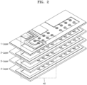
FIGS. 2 and3 schematically show a connector according to embodiments of the present disclosure; and -
FIG. 4 is a view for describing a spark gap according to embodiments of the present disclosure. - In the drawing figures, the dimensions of layers and regions may be exaggerated or reduced for clarity of illustration. It will also be understood that if a layer or element is referred to as being "on" another layer or substrate, it can be directly on the other layer or substrate, or intervening layers may also be present. Further, it will be understood that if a layer is referred to as being "under" another layer, it can be directly under, and one or more intervening layers may also be present. In addition, it will also be understood that if a layer is referred to as being "between" two layers, it can be the only layer between the two layers, or one or more intervening layers may also be present. Like reference numerals refer to like elements throughout.
- Expressions such as "at least one of," if preceding a list of components, modify the entire list of components and do not modify the individual components of the list.
- In the following embodiments, an x-axis, a y-axis, and a z-axis are not limited to three axes on an orthogonal coordinate system, and may be interpreted in a broad sense including them. For example, the x-axis, the y-axis, and the z-axis may be orthogonal to each other, but may also refer to different directions that are not orthogonal to each other.
-
FIG. 1 is a view for describing a connector according to embodiments of the present disclosure. - Referring to
FIG. 1 , an example of a connector of a (1-Layer) structure is shown. For example, the connector may include connector pins inserted therein and arranged in a 2-column array structure. - The connector may include a plurality of
connector holes 10 having a 2-column array structure into which the connector pins may be inserted. - Referring to
FIG. 1 , the connector may include aspark gap 20 between at least oneconnector hole 10 of the plurality ofconnector holes 10 andground 60 of a printed circuit board. - The connector may include a
conductor line 50 having an end connected to at least oneconnector hole 10. For example, referring toFIG. 1 , theconductor line 50 may be connected to the at least oneconnector hole 10 and thus electrically connected to the connector pin. In a case of a connector with a structure of two or more columns including theconductor line 50, applying thespark gap 20 may be difficult due to an arrangement of theconductor line 50. For example, referring toFIG. 1 , in the case of the connector having the structure of two or more columns, theconductor line 50 may be formed between the at least oneconnector hole 10 and theground 60 of the printed circuit board such that the at least oneconnector hole 10 to which thespark gap 20 is not applied may be formed. In this case, if anESD 30 is applied to the connector pin inserted into theconnector hole 10 to which thespark gap 20 is not applied, a circuit board or components may be damaged by theESD 30. -
FIGS. 2 and3 schematically show a connector according to embodiments of the present disclosure. - Referring to
FIG. 2 , a connector including four layers according to embodiments of the present disclosure is shown. It will be understood that more or fewer layers may be present. Referring toFIG. 3 , an enlarged view of apartial section 40 of the connector ofFIG. 2 is shown. For example, referring to apartial section 45 ofFIG. 3 , for theconnector hole 10 not including thespark gap 20 in a first layer (1-Layer), the connector including thespark gap 20 in a second layer (2-Layer), a third layer (3-Layer), and a fourth layer (4-Layer) is shown. - In one layer of a connector including connector holes having a structure of two or more columns, the
connector hole 10 to which thespark gap 20 is not applied may be formed. However, the connector according to embodiments of the present disclosure, including a multilayer structure, may form a spark gap in another layer for theconnector hole 10 to which thespark gap 20 is not applied, thereby preventing damage caused by an ESD. - Referring to
FIGS. 1 and2 , the connector according to embodiments of the present disclosure may be mounted on a printed circuit board. For example, a BMS circuit board according to embodiments of the present disclosure may include a printed circuit board having the connector according to the present disclosure mounted thereon. A battery pack according to embodiments of the present disclosure may include the printed circuit board having the connector according to the present disclosure mounted thereon. - The connector according to embodiments of the present disclosure may include the first layer (1-Layer) and the second layer (2-Layer). Herein, each of the first layer (1-Layer) and the second layer (2-Layer) may indicate one layer of the connector. Each of the first layer (1-Layer) and the second layer (2-Layer) may also indicate one layer of the printed circuit board. In this case, the connector according to embodiments of the present disclosure may indicate a connector of a structure where two layers may be stacked.
- The first layer (1-Layer) may include the plurality of connector holes 10 having an array structure of two or more columns allowing the connector pin to be inserted thereinto. For example, referring to
FIGS. 1 and2 , the first layer (1-Layer) may include the plurality of connector holes 10 having a 2-column array structure allowing the connector pin to be inserted thereinto. However, the present disclosure is not limited thereto, and the connector according to embodiments of the present disclosure may include the plurality of connector holes 10 having an array structure of two or more columns, such as three or four columns, etc. - The first layer (1 -Layer) may include the
spark gap 20 between the at least oneconnector hole 10 and theground 60 of the printed circuit board. A detailed description of thespark gap 20 will be provided later. - The first layer (1-Layer) may include the
conductor line 50 having an end connected to the at least oneconnector hole 10. For example, theconductor line 50 may be a conductive pattern formed on the printed circuit board. - The second layer (2-Layer) may be arranged to be stacked on a surface (e.g., a top surface in the orientation of
FIG. 2 ) of the first layer (1-Layer). For example, referring toFIG. 2 , the second layer (2-Layer) may be arranged in parallel with the first layer (1-Layer) in such a way to be stacked under the first layer (1-Layer). The second layer (2-Layer) may be arranged in parallel with the first layer (1-Layer) in such a way to be stacked on the first layer (1 -Layer). - The second layer (2-Layer) may include the plurality of connector holes 10 orthogonally spaced from and corresponding to (e.g., lined up with) the plurality of connector holes 10 of the first layer (1-Layer). For example, referring to
FIG. 2 , the second layer (2-Layer) may include the plurality of connector holes 10 spaced from and corresponding to the plurality of connector holes 10 of the first layer (1-Layer) in a y-axis direction (e.g., if an x-axis is a major axis of the first layer (1-Layer)) orthogonal to the first layer (1-Layer). For example, the plurality of connector holes 10 may be formed to penetrate the first layer (1-Layer) and the second layer (2-Layer). In this case, the connector pin may be inserted into theconnector hole 10 penetrating the first layer (1-Layer) and the second layer (2-Layer). - The second layer (2-Layer) may include the
spark gap 20 between theconnector hole 10 to correspond to the at least oneconnector hole 10 of the first layer (1-Layer), among the plurality of connector holes 10 of the second layer (2-Layer), and theground 60 of the printed circuit board. For example, referring toFIGS. 2 and3 , the second layer (2-Layer) may include thespark gap 20 between the ground of the printed circuit board and the (or each)connector hole 10 of the second layer (2-Layer) corresponding to the (or each)connector hole 10 of the first layer (1-Layer) to which a spark gap is not applied due to the arrangement of theconductor line 50 between theground 60 of the printed circuit board and the (or each)connector hole 10 of the first layer (1-Layer). More specifically, for theconnector hole 10 of the second layer (2-Layer) corresponding to the (or each)connector hole 10 of the first layer (1-Layer) to which the spark gap is not applied due to the arrangement of theconductor line 50 between theground 60 of the printed circuit board and the (or each)connector hole 10 of the first layer (1-Layer), the spark gap not included on the first layer (1-Layer) may be provided on the second layer (2-Layer). - The connector according to embodiments of the present disclosure may further include a third layer (3-Layer). In this case, the connector according to embodiments of the present disclosure may indicate a connector having a structure where three layers including the first layer (1-Layer) to the third layer (3-Layer) may be stacked.
- The third layer (3-Layer) may be arranged to be stacked with the first layer (1-Layer) and the second layer (2-Layer). For example, referring to
FIG. 2 , the third layer (3-Layer) may be arranged in parallel with the first layer (1-Layer) and the second layer (2-Layer) in such a way to be stacked under the first layer (1-Layer) and the second layer (2-Layer). The third layer (3-Layer) may be arranged in parallel with the first layer (1-Layer) and the second layer (2-Layer) in such a way to be stacked on the first layer (1-Layer) and the second layer (2-Layer). - The third layer (3-Layer) may include the plurality of connector holes 10 orthogonally spaced from and corresponding to the plurality of connector holes 10 of each of the first layer (1-Layer) and the second layer (2-Layer). For example, referring to
FIG. 2 , the third layer (3-Layer) may include the plurality of connector holes 10 spaced from and corresponding to the plurality of connector holes 10 of each of the first layer (1-Layer) and the second layer (2-Layer) in a y-axis direction (e.g., if the major axis of the first layer (1-Layer) is the x-axis) orthogonal to the first layer (1-Layer) and the second layer (2-Layer). For example, the plurality of connector holes 10 may be formed to penetrate the first layer (1-Layer), the second layer (2-Layer), and the third layer (3-Layer). In this case, the connector pin may be inserted into theconnector hole 10 penetrating the first layer (1-Layer), the second layer (2-Layer), and the third layer (3-Layer). - The third layer (3-Layer) may include the
spark gap 20 between theconnector hole 10 corresponding to the at least oneconnector hole 10 of the first layer (1-Layer), among the plurality of connector holes 10 of the third layer (3-Layer), and theground 60 of the printed circuit board. For example, referring toFIGS. 2 and3 , the third layer (3-Layer) may include thespark gap 20 between theground 60 of the printed circuit board and the (or each)connector hole 10 of the third layer (3-Layer) corresponding to the (or each)connector hole 10 of the first layer (1-Layer) to which thespark gap 20 is not applied due to the arrangement of theconductor line 50 between theground 60 of the printed circuit board and the (or each)connector hole 10 of the first layer (1-Layer). More specifically, for theconnector hole 10 of the third layer (3-Layer) corresponding to the (or each)connector hole 10 of the first layer (1-Layer) to which thespark gap 20 is not applied due to the arrangement of theconductor line 50 between theground 60 of the printed circuit board and the (or each)connector hole 10 of the first layer (1-Layer), thespark gap 20 not included on the first layer (1-Layer) may be provided on the third layer (3-Layer). In this case, thespark gap 20 not provided on the first layer (1-Layer) may be provided on the second layer (2-Layer) and the third layer (3-Layer), thereby dually preventing a damage from occurring due to an ESD. - The connector according to embodiments of the present disclosure may further include the fourth layer (4-Layer). In this case, the connector according to embodiments of the present disclosure may provide a connector having a structure where four layers including the first layer (1-Layer) to the fourth layer (4-Layer) may be stacked.
- The fourth layer (4-Layer) may be stacked with the first layer (1-Layer), the second layer (2-Layer), and the third layer (3-Layer). For example, referring to
FIG. 2 , the fourth layer (4-Layer) may be arranged in parallel with the first layer (1-Layer), the second layer (2-Layer), and the third layer (3-Layer) in such a way to be stacked under the first layer (1-Layer), the second layer (2-Layer), and the third layer (3-Layer). The fourth layer (4-Layer) may be arranged in parallel with the first layer (1-Layer), the second layer (2-Layer), and the third layer (3-Layer) in such a way to be stacked on the first layer (1-Layer), the second layer (2-Layer), and the third layer (3-Layer). - The fourth layer (4-Layer) may include the plurality of connector holes 10 orthogonally spaced from and corresponding to the plurality of connector holes 10 of each of the first layer (1-Layer), the second layer (2-Layer), and the third layer (3-Layer). For example, referring to
FIG. 2 , the fourth layer (4-Layer) may include the plurality of connector holes 10 spaced from and corresponding to the plurality of connector holes 10 of each of the first layer (1-Layer), the second layer (2-Layer), and the third layer (3-Layer) in the y-axis direction (e.g., if the major axis of the first layer is the x-axis) orthogonal to the first layer (1-Layer), the second layer (2-Layer), and the third layer (3-Layer). For example, the plurality of connector holes 10 may be formed to penetrate the first layer (1-Layer), the second layer (2-Layer), the third layer (3-Layer), and the fourth layer (4-Layer). In this case, the connector pin may be inserted into theconnector hole 10 penetrating the first layer (1-Layer), the second layer (2-Layer), the third layer (3-Layer), and the fourth layer (4-Layer). - The fourth layer (4-Layer) may include the
spark gap 20 between theconnector hole 10 corresponding to the at least oneconnector hole 10 of the first layer (1-Layer), among the plurality of connector holes 10 of the fourth layer (4-Layer), and theground 60 of the printed circuit board. For example, referring toFIGS. 2 and3 , the fourth layer (4-Layer) may include thespark gap 20 between theground 60 of the printed circuit board and the (or each)connector hole 10 of the fourth layer (4-Layer) corresponding to the (or each)connector hole 10 of the first layer (1-Layer) to which a spark gap is not applied due to the arrangement of theconductor line 50 between theground 60 of the printed circuit board and the (or each)connector hole 10 of the first layer (1-Layer). More specifically, for theconnector hole 10 of the fourth layer (4-Layer) corresponding to the (or each)connector hole 10 of the first layer (1-Layer) to which thespark gap 20 is not applied due to the arrangement of theconductor line 50 between theground 60 of the printed circuit board and the (or each)connector hole 10 of the first layer (1-Layer), thespark gap 20 not included on the first layer (1-Layer) may be provided on the fourth layer (4-Layer). In this case, thespark gap 20 not provided on the first layer (1-Layer) may be provided on the second layer (2-Layer), the third layer (3-Layer), and the fourth layer (4-Layer), thereby triply preventing a damage from occurring due to an ESD. -
FIG. 4 is a view for describing a spark gap according to embodiments of the present disclosure. - Referring to
FIG. 4 , thespark gap 20 according to embodiments of the present disclosure may include a gap between theconnector hole 10 having an ESD protection function and theground 60 of the printed circuit board. - For example, referring to
FIG. 4 , thespark gap 20 may include a gap between aground protruding portion 23 connected to theground 60 of the printed circuit board and ahole protruding portion 25 connected to theconnector hole 10 in a shape corresponding to theground protruding portion 23. - For example, the
ground protruding portion 23 and thehole protruding portion 25 may each include a copper foil layer in a triangular patch shape facing or pointing to each other. - According to embodiments of the present disclosure, if the
connector hole 10 is surrounded by theconductor line 50, thespark gap 20 may not be arranged on the first layer (1 -Layer), such that the connector according to embodiments of the present disclosure may include thespark gap 20 on the second to fourth layers (2-Layer to 4-Layer), thereby preventing a damage from occurring due to an ESD. - Although the present disclosure has been described with reference to an example shown in the drawings, it will be understood by those of ordinary skill in the art that various modifications and equivalent other examples may be made from the shown example within the scope of the appended claims.
- Those of ordinary skill in the art to which the present disclosure pertains will appreciate that the present disclosure may be implemented in different detailed ways without departing from the essential characteristics of the present disclosure. Accordingly, the aforementioned embodiments should be construed as being only illustrative, but should not be constructed as being restrictive from all aspects. For example, each element described as a single type may be implemented in a distributed manner, and likewise, elements described as being distributed may be implemented as a coupled type.
- The scope of the present disclosure is defined by the following claims rather than the detailed description, and the meanings and scope of the claims and all changes or modified forms derived from their equivalents should be construed as falling within the scope of the present disclosure.
- According to the present disclosure, by applying a spark gap to a connector with a structure of two or more columns, resistance to chronic ESD problems may be strengthened, and ESD reduction components such as an ESD capacitor, TVS, etc., may be reduced. However, the scope of the present disclosure is not limited by these effects.
- Example embodiments have been disclosed herein, and although specific terms may be employed, they are used and are to be interpreted in a generic and descriptive sense only and not for purpose of limitation. In some instances, as would be apparent to one of ordinary skill in the art as of the filing of the present application, features, characteristics, and/or elements described in connection with a particular embodiment may be used singly or in combination with features, characteristics, and/or elements described in connection with other embodiments unless otherwise specifically indicated. Accordingly, it will be understood by those of skill in the art that various changes in form and details may be made without departing from the scope of the present invention as set forth in the following claims.
Claims (13)
- A connector mounted on a printed circuit board, the connector comprising:a first layer including:a plurality of connector holes having an array structure of two or more columns allowing connector pins to be inserted thereinto;a spark gap between at least one connector hole of the plurality of connector holes and a ground of a printed circuit board; anda conductor line having an end connected to the at least one connector hole, the conductor line being arranged between the ground of the printed circuit board and the at least one connector hole; anda second layer stacked on a surface of the first layer, the second layer including:a plurality of connector holes orthogonally spaced from and corresponding to the plurality of connector holes of the first layer; anda spark gap between a connector hole, among the plurality of connector holes of the second layer, corresponding to the at least one connector hole of the first layer, and a ground of the printed circuit board.
- The connector as claimed in claim 1, further comprising a third layer stacked with the first layer and the second layer, the third layer including a plurality of connector holes orthogonally spaced from and corresponding to the plurality of connector holes of the first layer and the plurality of connector holes of the second layer.
- The connector as claimed in claim 2, wherein the third layer includes a spark gap between a connector hole, among the plurality of connector holes of the third layer, corresponding to the at least one connector hole of the first layer, and the ground of the printed circuit board.
- The connector as claimed in claim 2 or 3, further comprising a fourth layer stacked with the first layer, the second layer, and the third layer, the fourth layer including a plurality of connector holes orthogonally spaced from and corresponding to the plurality of connector holes of the first layer, the plurality of connector holes of the second layer, and the plurality of connector holes of the third layer.
- The connector as claimed in claim 4, wherein the fourth layer includes a spark gap between a connector hole, among the plurality of connector holes of the fourth layer, corresponding to the at least one connector hole of the first layer, and the ground of the printed circuit board.
- The connector as claimed in any preceding claim, wherein the spark gap comprises a gap between each of the plurality of connector holes having an electrostatic discharge protection function and the ground of the printed circuit board.
- The connector as claimed in claim 6, wherein the spark gap includes a gap between a ground protruding portion connected to the ground of the printed circuit board and a hole protruding portion protruding from a connector hole in a shape corresponding to the ground protruding portion.
- The connector as claimed in claim 7, wherein the ground protruding portion and the hole protruding portion each include a copper foil layer in a triangular patch shape facing each other.
- A battery management system circuit board including the connector as claimed in any preceding claim.
- A battery pack including the battery management system circuit board as claimed in claim 9.
- A multi-layer connector, comprising:a first printed circuit board layer having a first plurality of connector holes in an array structure of two or more columns allowing connector pins to be inserted thereinto;a first electrically conductive member coupled to the first printed circuit board layer at one or more first connector holes of the first plurality of connector holes, the first electrically conductive member being spaced apart from a second electrically conductive member connected to a ground of the first printed circuit board layer so as to create a first spark gap;a second printed circuit board layer stacked on a surface of the first printed circuit board layer, the second printed circuit board layer having a second plurality of connector holes orthogonally spaced from and lined up with the first plurality of connector holes; anda third electrically conductive member coupled to the second printed circuit board layer at one or more second connector holes of the second plurality of connector holes, the third electrically conductive member being spaced apart from a fourth electrically conductive member connected to a ground of the first printed circuit board layer so as to create a second spark gap.
- The multi-layer connector as claimed in claim 11, further comprising:a third printed circuit board layer stacked with the first printed circuit board layer and the second circuit board layer, the third printed circuit board layer including a third plurality of connector holes orthogonally spaced from and lined up with the first plurality of connector holes and the second plurality of connector holes; anda fifth electrically conductive member coupled to the third printed circuit board layer at one or more third connector holes of the third plurality of connector holes, the fifth electrically conductive member being spaced apart from a sixth electrically conductive member connected to a ground of the third printed circuit board layer so as to create a third spark gap.
- The multi-layer connector as claimed in claim 12, further comprising:a fourth printed circuit board layer stacked with the first printed circuit board layer, the second circuit board layer and the third circuit board layer, the fourth printed circuit board layer including a fourth plurality of connector holes orthogonally spaced from and lined up with the first plurality of connector holes, the second plurality of connector holes and the third plurality of connector holes; anda seventh electrically conductive member coupled to the fourth printed circuit board layer at one or more fourth connector holes of the fourth plurality of connector holes, the seventh electrically conductive member being spaced apart from an eighth electrically conductive member connected to a ground of the fourth printed circuit board layer so as to create a fourth spark gap.
Applications Claiming Priority (1)
| Application Number | Priority Date | Filing Date | Title |
|---|---|---|---|
| KR1020230132457A KR20250049703A (en) | 2023-10-05 | 2023-10-05 | Multistructure connector with spark gap |
Publications (1)
| Publication Number | Publication Date |
|---|---|
| EP4535929A1 true EP4535929A1 (en) | 2025-04-09 |
Family
ID=93010786
Family Applications (1)
| Application Number | Title | Priority Date | Filing Date |
|---|---|---|---|
| EP24204498.0A Pending EP4535929A1 (en) | 2023-10-05 | 2024-10-03 | Multi-structure connector including spark gap |
Country Status (4)
| Country | Link |
|---|---|
| US (1) | US20250118911A1 (en) |
| EP (1) | EP4535929A1 (en) |
| KR (1) | KR20250049703A (en) |
| CN (1) | CN119786999A (en) |
Citations (7)
| Publication number | Priority date | Publication date | Assignee | Title |
|---|---|---|---|---|
| GB2344615A (en) * | 1998-12-11 | 2000-06-14 | Kigass Electronics Ltd | Capacitive discharge ignition system with shunt track on printed circuit board |
| US20080266730A1 (en) * | 2007-04-25 | 2008-10-30 | Karsten Viborg | Spark Gaps for ESD Protection |
| US20090180225A1 (en) * | 2008-01-10 | 2009-07-16 | Industrial Technology Research Institute | Esd protection structure |
| US20090200063A1 (en) * | 2008-02-08 | 2009-08-13 | Sony Ericsson Mobile Communications Ab | Embedded spark gap |
| US20180088155A1 (en) * | 2016-09-27 | 2018-03-29 | Analog Devices Global Unlimited Company | Electrical overstress detection device |
| US20210151804A1 (en) * | 2018-12-26 | 2021-05-20 | Lg Chem, Ltd. | Battery Module Having Connector Mounted on FPCB, and Battery Pack and Vehicle Comprising Same |
| US20220077556A1 (en) * | 2019-07-05 | 2022-03-10 | Murata Manufacturing Co., Ltd. | Transmission line and electronic device |
-
2023
- 2023-10-05 KR KR1020230132457A patent/KR20250049703A/en active Pending
-
2024
- 2024-07-23 US US18/780,625 patent/US20250118911A1/en active Pending
- 2024-09-20 CN CN202411312421.8A patent/CN119786999A/en active Pending
- 2024-10-03 EP EP24204498.0A patent/EP4535929A1/en active Pending
Patent Citations (7)
| Publication number | Priority date | Publication date | Assignee | Title |
|---|---|---|---|---|
| GB2344615A (en) * | 1998-12-11 | 2000-06-14 | Kigass Electronics Ltd | Capacitive discharge ignition system with shunt track on printed circuit board |
| US20080266730A1 (en) * | 2007-04-25 | 2008-10-30 | Karsten Viborg | Spark Gaps for ESD Protection |
| US20090180225A1 (en) * | 2008-01-10 | 2009-07-16 | Industrial Technology Research Institute | Esd protection structure |
| US20090200063A1 (en) * | 2008-02-08 | 2009-08-13 | Sony Ericsson Mobile Communications Ab | Embedded spark gap |
| US20180088155A1 (en) * | 2016-09-27 | 2018-03-29 | Analog Devices Global Unlimited Company | Electrical overstress detection device |
| US20210151804A1 (en) * | 2018-12-26 | 2021-05-20 | Lg Chem, Ltd. | Battery Module Having Connector Mounted on FPCB, and Battery Pack and Vehicle Comprising Same |
| US20220077556A1 (en) * | 2019-07-05 | 2022-03-10 | Murata Manufacturing Co., Ltd. | Transmission line and electronic device |
Also Published As
| Publication number | Publication date |
|---|---|
| CN119786999A (en) | 2025-04-08 |
| US20250118911A1 (en) | 2025-04-10 |
| KR20250049703A (en) | 2025-04-14 |
Similar Documents
| Publication | Publication Date | Title |
|---|---|---|
| US11387016B2 (en) | Transmission line substrate and electronic device | |
| US6819543B2 (en) | Multilayer capacitor with multiple plates per layer | |
| US5313416A (en) | Semiconductor memory control device and method of mounting same in high density | |
| US9549467B1 (en) | Printed circuit board assembly for use in space missions | |
| EP2654387B1 (en) | Printed circuit board | |
| US20070127175A1 (en) | Devices and System for Electrostatic Discharge Suppression | |
| US7972143B2 (en) | Printed circuit assembly | |
| US20080158773A1 (en) | Multilayer capacitor array | |
| CN101998754A (en) | Electrostatic discharge protection structure and electronic device using same | |
| EP2785155B1 (en) | Circuit board and electronic device | |
| US9748042B2 (en) | Multilayer feedthrough capacitor | |
| US7086869B1 (en) | Flexible cable interconnect with integrated EMC shielding | |
| US20080248687A1 (en) | Internally Overlapped Conditioners | |
| CN205985430U (en) | A interconnect equipment and electronic equipment for electronic equipment | |
| US9974159B2 (en) | Eggcrate radio frequency interposer | |
| JP2006128633A (en) | Multi-terminal element and printed wiring board | |
| US20030147226A1 (en) | Method and structure for reduction of impedance using decoupling capacitor | |
| EP4535929A1 (en) | Multi-structure connector including spark gap | |
| US7411775B2 (en) | Feedthrough multilayer capacitor array | |
| US7405473B1 (en) | Techniques for optimizing electrical performance and layout efficiency in connectors with via placement and routing | |
| JPH07161568A (en) | Multilayer capacitor array | |
| EP4507459A1 (en) | Circuit board and circuit board assembly | |
| US20080013295A1 (en) | Capacitor sheet and electronic circuit board | |
| DE102018215495A1 (en) | Conductor connection structure for plate-like routing elements | |
| US8964407B2 (en) | Substrate with built-in electronic component |
Legal Events
| Date | Code | Title | Description |
|---|---|---|---|
| PUAI | Public reference made under article 153(3) epc to a published international application that has entered the european phase |
Free format text: ORIGINAL CODE: 0009012 |
|
| STAA | Information on the status of an ep patent application or granted ep patent |
Free format text: STATUS: REQUEST FOR EXAMINATION WAS MADE |
|
| 17P | Request for examination filed |
Effective date: 20241003 |
|
| AK | Designated contracting states |
Kind code of ref document: A1 Designated state(s): AL AT BE BG CH CY CZ DE DK EE ES FI FR GB GR HR HU IE IS IT LI LT LU LV MC ME MK MT NL NO PL PT RO RS SE SI SK SM TR |