EP4535569A1 - Electromagnetic wave reflection device, electromagnetic wave reflection fence, and reflection panel - Google Patents
Electromagnetic wave reflection device, electromagnetic wave reflection fence, and reflection panel Download PDFInfo
- Publication number
- EP4535569A1 EP4535569A1 EP23815689.7A EP23815689A EP4535569A1 EP 4535569 A1 EP4535569 A1 EP 4535569A1 EP 23815689 A EP23815689 A EP 23815689A EP 4535569 A1 EP4535569 A1 EP 4535569A1
- Authority
- EP
- European Patent Office
- Prior art keywords
- layer
- conductive pattern
- reflection
- electromagnetic wave
- intermediate layer
- Prior art date
- Legal status (The legal status is an assumption and is not a legal conclusion. Google has not performed a legal analysis and makes no representation as to the accuracy of the status listed.)
- Pending
Links
Images







Classifications
-
- H—ELECTRICITY
- H01—ELECTRIC ELEMENTS
- H01Q—ANTENNAS, i.e. RADIO AERIALS
- H01Q15/00—Devices for reflection, refraction, diffraction or polarisation of waves radiated from an antenna, e.g. quasi-optical devices
- H01Q15/0006—Devices acting selectively as reflecting surface, as diffracting or as refracting device, e.g. frequency filtering or angular spatial filtering devices
- H01Q15/0013—Devices acting selectively as reflecting surface, as diffracting or as refracting device, e.g. frequency filtering or angular spatial filtering devices said selective devices working as frequency-selective reflecting surfaces, e.g. FSS, dichroic plates, surfaces being partly transmissive and reflective
-
- H—ELECTRICITY
- H01—ELECTRIC ELEMENTS
- H01Q—ANTENNAS, i.e. RADIO AERIALS
- H01Q15/00—Devices for reflection, refraction, diffraction or polarisation of waves radiated from an antenna, e.g. quasi-optical devices
- H01Q15/14—Reflecting surfaces; Equivalent structures
-
- H—ELECTRICITY
- H01—ELECTRIC ELEMENTS
- H01Q—ANTENNAS, i.e. RADIO AERIALS
- H01Q15/00—Devices for reflection, refraction, diffraction or polarisation of waves radiated from an antenna, e.g. quasi-optical devices
- H01Q15/0006—Devices acting selectively as reflecting surface, as diffracting or as refracting device, e.g. frequency filtering or angular spatial filtering devices
- H01Q15/0013—Devices acting selectively as reflecting surface, as diffracting or as refracting device, e.g. frequency filtering or angular spatial filtering devices said selective devices working as frequency-selective reflecting surfaces, e.g. FSS, dichroic plates, surfaces being partly transmissive and reflective
- H01Q15/0026—Devices acting selectively as reflecting surface, as diffracting or as refracting device, e.g. frequency filtering or angular spatial filtering devices said selective devices working as frequency-selective reflecting surfaces, e.g. FSS, dichroic plates, surfaces being partly transmissive and reflective said selective devices having a stacked geometry or having multiple layers
-
- H—ELECTRICITY
- H01—ELECTRIC ELEMENTS
- H01Q—ANTENNAS, i.e. RADIO AERIALS
- H01Q15/00—Devices for reflection, refraction, diffraction or polarisation of waves radiated from an antenna, e.g. quasi-optical devices
- H01Q15/0006—Devices acting selectively as reflecting surface, as diffracting or as refracting device, e.g. frequency filtering or angular spatial filtering devices
- H01Q15/0086—Devices acting selectively as reflecting surface, as diffracting or as refracting device, e.g. frequency filtering or angular spatial filtering devices said selective devices having materials with a synthesized negative refractive index, e.g. metamaterials or left-handed materials
Definitions
- the present invention relates to an electromagnetic wave reflecting device, an electromagnetic wave reflecting fence, and a reflection panel.
- NLOS non-line-of-sight
- a metasurface consists of a periodic structure or pattern finer than a wavelength, and is designed to reflect radio waves in a desired direction (for example, see Non-Patent Document 1).
- a metasurface itself is realized by a periodically repeated fine structure or metal pattern; in actual manufacturing of metasurfaces, a metal pattern is often provided on one surface of a dielectric substrate, and a ground layer is often provided on the opposite surface.
- a metal pattern and a ground layer are often made of a metal having good conductivity, such as copper (Cu), nickel (Ni), or silver (Ag).
- a metal pattern or a ground layer provided to a reflection panel of an electromagnetic wave reflecting device by applying a metasurface to the reflection panel a chemical reaction product, such as rust, is caused due to the influence of oxygen or moisture.
- a reflective surface including a metasurface functions through its metal pattern, and the reflection angle and the reflection efficiency are determined by the surface state of the metal, the size, the shape, the arrangement, the resistance value of the unit pattern, and the like.
- an electromagnetic wave reflecting device includes a reflection panel configured to reflect radio waves in a desired band selected from a band of frequencies equal to or higher than 1 GHz and equal to or lower than 170 GHz, and a frame that holds the reflection panel, wherein the reflection panel includes: a dielectric layer; a periodic conductive pattern provided on one surface of the dielectric layer; a ground layer provided on the other surface of the dielectric layer; a first intermediate layer covering the conductive pattern; a first dielectric substrate bonded to the conductive pattern by the first intermediate layer; a second intermediate layer covering the ground layer; and a second dielectric substrate bonded to the ground layer by the second intermediate layer.
- the reflection efficiency of the electromagnetic wave reflecting device is 60% or more, preferably 70% or more.
- a conductive pattern and a ground layer provided on a reflection panel are respectively covered with intermediate layers and bonded to a dielectric substrate.
- a transmittance of the intermediate layer for electromagnetic waves of a frequency used is 60% or more, preferably 70% or more, and more preferably 80% or more.
- FIG. 1 is a schematic diagram of an electromagnetic wave reflecting fence 100 in which a plurality of electromagnetic wave reflecting devices 60-1, 60-2, and 60-3 are joined.
- FIG. 1 illustrates the electromagnetic wave reflecting fence 100 configured by three electromagnetic wave reflecting devices 60-1, 60-2, and 60-3 joined to each other (hereinafter, they may be collectively referred to as "electromagnetic wave reflecting devices 60" as appropriate), the number of the electromagnetic wave reflecting devices 60 to be joined is not particularly limited.
- the conductive film may be formed in a periodic pattern, a mesh pattern, a geometric pattern, a transparent film, or the like.
- Making the layer structure of the reflection panel specific improves the weather resistance and suppresses the deterioration of the reflection characteristics.
- the reflection efficiency of the electromagnetic wave reflecting devices 60 is improved by keeping the occupancy of the conductive pattern in the reflective surface within a predetermined range.
- Each of the reflection panels 10-1, 10-2, and 10-3 may have a specular reflection surface in which an angle of incidence and an angle of emergence of the electromagnetic wave are equal, or may be a non-specular reflection surface in which an angle of incidence and an angle of reflection are different from each other.
- the non-specular reflection surface includes a metasurface which is an artificial reflection surface designed to reflect radio waves in a desired direction, in addition to a diffusion surface and a scattering surface.
- the reflection panels 10-1, 10-2, and 10-3 are preferably electrically connected to each other; in the case where the neighboring reflection panels 10 include a metasurface, on the other hand, electrical connections between the neighboring reflection panels 10 may be unnecessary.
- the neighboring reflection panels 10 are held and connected in the X direction by the frames 50, and an electromagnetic wave reflecting fence 100 is thereby obtained.
- the electromagnetic wave reflecting device 60 may include legs 56 for supporting the frame 50 in addition to the reflection panel 10 and the frame 50. As illustrated in FIG. 1 , in order to set the electromagnetic wave reflecting device 60 or the electromagnetic wave reflecting fence 100 upright on the installation surface, it is desirable to provide the legs 56, but the legs 56 are not essential.
- a top frame 57 for holding the upper end of the reflection panel 10 and a bottom frame 58 for holding the lower end of the reflection panel 10 may be used.
- the frame 50, the top frame 57, and the bottom frame 58 constitute a frame that holds the entire periphery of the reflection panel 10.
- the frame 50 may be referred to as a "side frame" due to its positional relationship with respect to the top frame 57 and the bottom frame 58.
- the electromagnetic wave reflecting device 60 may be installed on a wall surface or a ceiling, with the reflection panel 10 being held by the frame 50, the top frame 57, and the bottom frame 58.
- FIG. 2 is a cross-sectional view of the frame 50 taken along line A-A of FIG. 1 , viewed in the section parallel to the XZ plane.
- the frame 50 includes a conductive main body 500 and slits 51 formed on both sides of the main body 500 in the width direction.
- the slits 51 hold the side edges of the reflection panel 10.
- the side edge of the reflection panel 10 is an edge along the Y direction in FIG. 1 .
- the main body 500 is provided with a cavity 52 communicating with the slit 51, a groove 53 provided in the cavity 52, and a hollow 55 not communicating with the cavity 52 and the groove 53; however, the present invention is not limited to this example.
- the groove 53 is provided at a position facing the slit 51 with the cavity 52 interposed therebetween, and holds the side edge of the reflection panel 10 inserted through the slit 51.
- the weight of the frame 50 can be reduced by providing the cavity 52 and the hollow 55 in the frame 50. Provision of the groove 53 in the cavity 52 reinforces the retention of the reflection panel 10.
- a non-conductive cover 501 such as a resin-made cover, may be provided on the outer surface of the main body 500 but the cover 501 is not essential. In the case where the cover 501 is provided, the cover 501 functions as a protection member that protects the frame 50.
- FIG. 3 is a cross-sectional view parallel to the XZ plane, illustrating the state of insertion of the reflection panel 10 into the frame 50.
- the reflection panels 10-1 and 10-2 are inserted from the slits 51 (see FIG. 2 ) on both sides of the main body 500.
- the reflection panels 10-1 and 10-2 may or may not abut on the main body 500 by being inserted into the groove 53 (see FIG. 2 ) of the cavity 52 to the depth.
- the reflection panels 10-1 and 10-2 are inserted into the slits 51, respectively, so that the neighboring reflection panels 10-1 and 10-2 can be stably held.
- the main body 500 may be partially made of a non-conductive material.
- FIG. 4 illustrates an example of a layer structure of the reflection panel 10.
- This layer structure is a layer structure in the thickness (Z) direction of the reflection panel 10.
- the reflection panel 10 has a dielectric layer 14, a conductive layer 15 provided on one surface of the dielectric layer 14, a ground layer 13 provided on the other surface, a first intermediate layer 16 covering the conductive layer 15, and a second intermediate layer covering the ground layer 13.
- the first intermediate layer 16 is an adhesive film
- the first dielectric substrate 17 is bonded to the first intermediate layer 16.
- the second intermediate layer 12 is an adhesive film, and the second dielectric substrate 11 is bonded to the second intermediate layer 12.
- the dielectric layer 14 is an insulating polymer film such as polycarbonate, cycloolefin polymer (COP), polyethylene terephthalate (PET), or fluorine resin, and has a thickness of about 0.3 mm to 1.0 mm.
- the dielectric layer 14 may be made of any material having a dielectric constant and a dielectric loss tangent suitable for realizing target reflection characteristics.
- the conductive layer 15 forms a reflective surface of the reflection panel 10.
- the reflective surface constituted by the conductive layer 15 may include a metasurface having artificially controlled reflective properties.
- the conductive layer 15 includes a conductive pattern 151 including a periodic pattern and an adhesive layer 152 that fixes the conductive pattern 151 to the dielectric layer 14.
- the conductive pattern 151 is made of a material having good conductivity, such as Cu, Ni, or Ag, and has a thickness of about 10 ⁇ m to 50 ⁇ m.
- the adhesive layer 152 is a material that can support the conductive pattern 151 and fix the same to the dielectric layer 14, and may be made of a thermoplastic resin, such as a vinyl acetate resin, an acrylic resin, a cellulose resin, or a silicone resin.
- the thickness of the adhesive layer 152 is about 5 ⁇ m to 50 ⁇ m.
- the first intermediate layer 16 covering the conductive layer 15 protects the surface of the conductive layer 15 and is used for bonding the first dielectric substrate 17.
- the first intermediate layer 16 preferably has durability and moisture resistance, and for example, ethylene-vinyl acetate (EVA) copolymer or cycloolefin polymer (COP) can be used.
- EVA ethylene-vinyl acetate
- COP cycloolefin polymer
- the thickness of the first intermediate layer 16 is 10 ⁇ m to 400 ⁇ m.
- the second intermediate layer 12 covering the conductive layer 13 protects the surface of the conductive layer 13 and is used for bonding the second dielectric substrate 11.
- the second intermediate layer 12 preferably has durability and moisture resistance, and for example, EVA or COP can be used.
- the thickness of the second intermediate layer 12 is 10 ⁇ m to 400 ⁇ m.
- the reflection characteristics are evaluated by changing the area occupancy of the conductive pattern 151 of the reflection panel 10 having the layer structure illustrated in FIG. 4 . It is expected that the reflection efficiency will be improved as the area occupancy of the conductive pattern 151 is increased.
- the electromagnetic wave reflecting device 60 is used indoors or outdoors, such as on a road, in a park, in a factory, in a commercial facility, or in an office, it is desirable that, from the viewpoint of taking in natural light or illumination light, the reflection panel 10 has a certain degree of transparency. For this reason, a design capable of maintaining high reflection efficiency while maintaining a transmittance of 35% or more, more preferably 40%, is aimed.
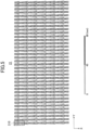
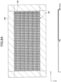
- FIG. 5 is a diagram illustrating a model 21 of the conductive pattern 151 used for evaluation of the reflection characteristics of the reflection panel 10.
- the model 21 for evaluation includes a periodic array of unit cells (also referred to as "supercells") 210.
- the unit cells 210 are arranged in six rows in the X direction and 36 columns in the Y direction, and constitute a metasurface that reflects electromagnetic waves at an angle different from an angle of incidence.
- FIG. 6 is a schematic diagram illustrating the structure of the unit cell 210 of the model 21.
- the unit cell 210 is constituted by six metal patches 211, 212, 213, 214, 215, and 216.
- the width (W) direction and the length (L) direction of the metal patches 211 through 216 correspond to the width (X) direction and the height (Y) direction of the reflection panel 10 of FIG. 1 , respectively.
- the metal patches 211 through 216 have the same width W and different lengths L but have the same central axis of the length (the Y coordinate positions of the central axis are the same).
- the pitch in the X direction is uniform.
- the evaluation method is as follows: a plane wave of 28.0 GHz is made incident at an incident angle of 0° in the layer structure of FIG. 4 , using the conductive pattern 151 of the model 21 of FIG. 5 , and the scattering cross section of the reflected wave is analyzed by general-purpose three-dimensional electromagnetic field simulation software.
- the scattering cross section namely a radar cross section (RCS), is used as an indicator of the ability to reflect incident electromagnetic waves.
- FIG. 7 shows an analysis space 101 of the electromagnetic wave simulation.
- the analysis space is expressed as (a dimension in the X direction) ⁇ (a dimension in the Y direction) ⁇ (a dimension in the Z direction).
- the dimensions of the analysis space 101 is 83.9 mm ⁇ 192.6 mm ⁇ 3.7 mm if the incident electromagnetic wave has a frequency of 28.0 GHz.
- the boundary condition is designed on an assumption that the electromagnetic wave absorber 102 is arranged around the analysis space 101.
- FIG. 8A is a schematic diagram of the XY plane of the analysis space 101 surrounded by the electromagnetic absorber 102
- FIG. 8B is a schematic diagram of the XZ plane of the analysis space 101
- FIG. 8C is a schematic diagram of the YZ plane of the analysis space 101.
- the power reflection efficiency is calculated by changing the size and the area occupancy of the metal patches of the model 21 constituting the conductive pattern 151.
- a polycarbonate film having a thickness of 0.7 mm is used as the dielectric layer 14.
- the ground layer 13 is provided on one of the surfaces of the polycarbonate film by an Ag-based multilayer film having a thickness of 0.36 mm, and the conductive layer 15 is provided on the other surface of the polycarbonate film.
- the conductive layer 15 has the conductive pattern 151 made of a copper film having a thickness of 0.03 mm formed on the adhesive layer 152 having a thickness of 0.01 mm.
- the shapes, namely the occupancy of the adhesive layer 152 and that of the conductive pattern 151 are the same.
- the intermediate layer 12 covering the ground layer 13 and the intermediate layer 16 covering the conductive layer 15 are both made of EVA having a thickness of 400 ⁇ m.
- a 2.0-mm polycarbonate sheet to serve as the dielectric substrates 11 and 17 is bonded to each of the intermediate layers 12 and 16.
- Six metallic patches 211 through 216 of the unit cell 210 of the conductive pattern 151 are formed in a rectangular shape having a uniform width W of 0.7 mm and respective lengths L of 2.8478 mm, 3.0043 mm, 3.7000 mm, 1.7348 mm, 2.5174 mm, and 2.6925 mm.
- the widthwise gap between the metallic patches is uniformly 1.6283 mm.
- the area occupancy of the conductive pattern 151 is 15.4%, and the transmittance of the entire layer structure illustrated in FIG. 4 is 55.5%.
- Six metallic patches 211 through 216 of the unit cell 210 of the conductive pattern 151 are formed in a rectangular shape having a uniform width W of 1.0 mm and respective lengths L of 2.8091 mm, 2.9861 mm, 3.7461 mm, 1.2505 mm, 2.3214 mm, and 2.5348 mm.
- the widthwise gap between the metallic patches is uniformly 1.3283 mm.
- the area occupancy of the conductive pattern 151 is 20.9%, and the transmittance of the entire layer structure is 51.9%.
- the gain value at 50° in the RCS plot in the case where a plane wave of 28.0 GHz incident at an angle of incidence of 0° is reflected at an angle of reflection of 50° is 11.6106 dB.
- Example 3 the layer structure is the same as that of Examples 1 and 2, but the size and the area occupancy of the conductive pattern 151 are changed from Examples 1 and 2.
- the ground layer 13 is provided on one of the surfaces of the polycarbonate film having a thickness of 0.7 mm, which serves as the dielectric layer 14, by an Ag-based multilayer film having a thickness of 0.36 mm, and the conductive layer 15 is provided on the other surface of the polycarbonate film.
- the conductive layer 15 has the conductive pattern 151 made of a copper film having a thickness of 0.03 mm formed on an adhesive layer 152 having a thickness of 0.01 mm.
- the shapes, namely the occupancy of the adhesive layer 152 and that of the conductive pattern 151 are the same.
- the intermediate layer 12 covering the ground layer 13 and the intermediate layer 16 covering the conductive layer 15 are both made of EVA having a thickness of 400 ⁇ m.
- a 2.0-mm polycarbonate sheet to serve as the dielectric substrates 11 and 17 is bonded to each of the intermediate layers 12 and 16.
- Six metallic patches 211 through 216 of the unit cell 210 of the conductive pattern 151 are formed in a rectangular shape having a uniform width W of 1.5 mm and respective lengths L of 2.6477 mm, 2.8607 mm, 4.0544 mm, 1.2510 mm, 2.1591 mm, and 2.3923 mm.
- the widthwise gap between the metallic patches is uniformly 0.8283 mm.
- the area occupancy of the conductive pattern 151 is 30.8%, and the transmittance of the entire layer structure is 46.0%.
- the gain value at 50° in the RCS plot in the case where a plane wave of 28.0 GHz incident at an angle of incidence of 0° is reflected at an angle of reflection of 50° is 11.5595 dB.
- Example 4 the layer structure is the same as that of Examples 1 through 3, but the size and the area occupancy of the conductive pattern 151 are changed from Examples 1 through 3.
- the ground layer 13 is provided on one of the surfaces of the polycarbonate film having a thickness of 0.7 mm, which serves as the dielectric layer 14, by an Ag-based multilayer film having a thickness of 0.36 mm, and the conductive layer 15 is provided on the other surface of the polycarbonate film.
- the conductive layer 15 has the conductive pattern 151 made of a copper film having a thickness of 0.03 mm formed on an adhesive layer 152 having a thickness of 0.01 mm.
- the shapes, namely the occupancy of the adhesive layer 152 and that of the conductive pattern 151 are the same.
- the intermediate layer 12 covering the ground layer 13 and the intermediate layer 16 covering the conductive layer 15 are both made of EVA having a thickness of 400 ⁇ m.
- a 2.0-mm polycarbonate sheet to serve as the dielectric substrates 11 and 17 is bonded to each of the intermediate layers 12 and 16.
- Six metallic patches 211 through 216 of the unit cell 210 of the conductive pattern 151 are formed in a rectangular shape having a uniform width W of 2.1 mm and respective lengths L of 2.6000 mm, 2.8354 mm, 3.5531 mm, 1.6459 mm, 2.1321 mm, and 2.3600 mm.
- the widthwise gap between the metallic patches is uniformly 0.2283 mm.
- the area occupancy of the conductive pattern 151 is 42.4%, and the transmittance of the entire layer structure is 38.8%.
- the gain value at 50° in the RCS plot in the case where a plane wave of 28.0 GHz incident at an angle of incidence of 0° is reflected at an angle of reflection of 50° is 11.6908 dB.
- Example 5 the same layer structure as that of Examples 1 through 4 and the same conductive pattern 151 as that of Example 4 are used, but the thickness of the Cu-made conductive pattern 151 supported by the adhesive layer 152 having a thickness of 0.01 mm is increased to 0.05 mm.
- the intermediate layer 16 covering the adhesive layer 152 and the conductive pattern 151 and the intermediate layer 12 covering the Ag-made ground layer 13 are both made of EVA having a thickness of 400 ⁇ m.
- a 2.0-mm polycarbonate sheet to serve as the dielectric substrates 11 and 17 is bonded to each of the intermediate layers 12 and 16.
- Six metallic patches 211 through 216 of the unit cell 210 of the conductive pattern 151 are, similarly to Example 4, formed in a rectangular shape having a uniform width W of 2.1 mm and respective lengths L of 2.6000 mm, 2.8354 mm, 3.5531 mm, 1.6459 mm, 2.1321 mm, and 2.3600 mm.
- the widthwise gap between the metallic patches is uniformly 0.2283 mm.
- the area occupancy of the conductive pattern 151 is 42.4%, and the transmittance of the entire layer structure is 38.8%.
- the gain value at 50° in the RCS plot in the case where a plane wave of 28.0 GHz incident at an angle of incidence of 0° is reflected at an angle of reflection of 50° is 11.7083 dB.
- Example 8 the same layer structure as that of Examples 1 through 7, the conductive pattern 151 having the same thickness and shape as those of Example 7, and the intermediate layers 16 and 12 having the same thickness as that of Example 7 are used, but the thickness of the dielectric substrates 17 and 11 bonded to the intermediate layers 16 and 12, respectively, is reduced to 1.0 mm.
- An EVA having a thickness of 100 ⁇ m is used as the intermediate layer 16 covering the adhesive layer 152 and the conductive pattern 151, and a polycarbonate sheet having a thickness of 1.0 mm is bonded to the intermediate layer 16.
- An EVA having a thickness of 100 ⁇ m is used as the intermediate layer 12 covering the Ag-made ground layer 13, and a polycarbonate sheet having a thickness of 1.0 mm is bonded to the intermediate layer 12.
- the area occupancy of the conductive pattern 151 is preferably 10% or more and 45% or less, more preferably 15% or more and 45% or less in order to maintain the transmittance at 35% or more and to maintain the power reflection efficiency at 60% or more, more preferably 70% or more.
- the thickness of the conductive pattern 151 in this case is 0.01 mm or more and 0.05 mm or less. This is considered to be because, in the case where the area occupancy of the conductive pattern 151 becomes less than 10%, the electric fields of the incident electromagnetic wave and the reflected wave are concentrated on the surrounding dielectric, and the reflection efficiency in the designed angle and direction is deteriorated.
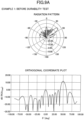
- FIG. 9A is a diagram illustrating a radiation pattern and an orthogonal coordinate plot of the reflection panel 10 having the layer structure of Example 1 and being in an initial state.
- FIG. 9B is a diagram illustrating a radiation pattern and an orthogonal coordinate plot of the reflection panel 10 of Example 1 after being left for 500 hours in an environment where the temperature is 60 °C and the humidity is 90%.
- a main peak is observed in a direction of +50°, and a side peak is observed in a direction of -50° with respect to the normal incidence.
- the reflected radio waves cover a range of 30° to 80° in the plus direction and the minus direction with respect to the normal incidence.
Landscapes
- Physics & Mathematics (AREA)
- Electromagnetism (AREA)
- Aerials With Secondary Devices (AREA)
- Shielding Devices Or Components To Electric Or Magnetic Fields (AREA)
Applications Claiming Priority (2)
| Application Number | Priority Date | Filing Date | Title |
|---|---|---|---|
| JP2022089848 | 2022-06-01 | ||
| PCT/JP2023/017289 WO2023233928A1 (ja) | 2022-06-01 | 2023-05-08 | 電磁波反射装置、電磁波反射フェンス、及び反射パネル |
Publications (1)
| Publication Number | Publication Date |
|---|---|
| EP4535569A1 true EP4535569A1 (en) | 2025-04-09 |
Family
ID=89026305
Family Applications (1)
| Application Number | Title | Priority Date | Filing Date |
|---|---|---|---|
| EP23815689.7A Pending EP4535569A1 (en) | 2022-06-01 | 2023-05-08 | Electromagnetic wave reflection device, electromagnetic wave reflection fence, and reflection panel |
Country Status (6)
| Country | Link |
|---|---|
| US (1) | US20250055201A1 (https=) |
| EP (1) | EP4535569A1 (https=) |
| JP (1) | JPWO2023233928A1 (https=) |
| KR (1) | KR20250018470A (https=) |
| CN (1) | CN119013844A (https=) |
| WO (1) | WO2023233928A1 (https=) |
Families Citing this family (2)
| Publication number | Priority date | Publication date | Assignee | Title |
|---|---|---|---|---|
| WO2025158773A1 (ja) * | 2024-01-26 | 2025-07-31 | Agc株式会社 | 電磁波反射パネル、電磁波反射装置、及び電磁波反射フェンス |
| CN119627451B (zh) * | 2025-01-23 | 2025-10-31 | 东南大学 | 一种宽角域隐身吸波超表面 |
Family Cites Families (5)
| Publication number | Priority date | Publication date | Assignee | Title |
|---|---|---|---|---|
| JP6930784B2 (ja) * | 2017-01-05 | 2021-09-01 | 住友電工プリントサーキット株式会社 | プリント配線用原板及びプリント配線板 |
| EP4131655B1 (en) * | 2020-03-31 | 2025-11-19 | Agc Inc. | Wireless transmission system |
| JP7048671B2 (ja) | 2020-06-10 | 2022-04-05 | 大王製紙株式会社 | 繊維状セルロース含有物、繊維状セルロース複合樹脂、及び繊維状セルロース含有物の製造方法 |
| JP7785474B2 (ja) * | 2020-09-29 | 2025-12-15 | 日東電工株式会社 | ミリ波アンテナ |
| JP7623820B2 (ja) * | 2020-10-30 | 2025-01-29 | 電気興業株式会社 | 可変リフレクトアレーおよび可変リフレクトアレーの設計方法 |
-
2023
- 2023-05-08 JP JP2024524273A patent/JPWO2023233928A1/ja active Pending
- 2023-05-08 CN CN202380033667.9A patent/CN119013844A/zh active Pending
- 2023-05-08 WO PCT/JP2023/017289 patent/WO2023233928A1/ja not_active Ceased
- 2023-05-08 KR KR1020247034280A patent/KR20250018470A/ko active Pending
- 2023-05-08 EP EP23815689.7A patent/EP4535569A1/en active Pending
-
2024
- 2024-10-22 US US18/923,582 patent/US20250055201A1/en active Pending
Also Published As
| Publication number | Publication date |
|---|---|
| KR20250018470A (ko) | 2025-02-06 |
| CN119013844A (zh) | 2024-11-22 |
| WO2023233928A1 (ja) | 2023-12-07 |
| JPWO2023233928A1 (https=) | 2023-12-07 |
| US20250055201A1 (en) | 2025-02-13 |
Similar Documents
| Publication | Publication Date | Title |
|---|---|---|
| US20250055201A1 (en) | Electromagnetic wave reflecting device, electromagnetic wave reflecting fence, and reflection panel | |
| EP4287405A1 (en) | Structure and construction material | |
| EP4160822B1 (en) | Antenna unit and window glass | |
| US20250096480A1 (en) | Electromagnetic wave reflecting device, electromagnetic wave reflecting fence, and reflection panel | |
| EP4475340A1 (en) | Radio wave reflector and construction material | |
| CN120435802A (zh) | 无线传输系统 | |
| KR20250006862A (ko) | 전자파 반사 장치 및 전자파 반사 펜스 | |
| WO2023003961A1 (en) | Method and system with fragmented metastructures formed with a plurality of metasurface arrays | |
| TW202425422A (zh) | 反射板、使用其之電磁波反射裝置及電磁波反射柵 | |
| US20250096479A1 (en) | Electromagnetic wave reflecting device, electromagnetic wave reflecting fence, and reflection panel | |
| WO2024106405A1 (ja) | 電波反射体、電波反射体の作製方法、電波反射構造体、電波反射システムおよび電波反射装置 | |
| CN209526201U (zh) | 宽频带双极化天线 | |
| JP2024021078A (ja) | 電波反射体、電波反射体の製造方法および電波反射体の施工方法 | |
| EP4459796A1 (en) | Radio wave reflector | |
| WO2023233921A1 (ja) | 電磁波反射装置、電磁波反射フェンス、及び反射パネル | |
| US20250309555A1 (en) | Reflection panel and electromagnetic-wave reflecting apparatus | |
| WO2024029365A1 (ja) | 反射パネル、これを用いた電磁波反射装置、及び電磁波反射フェンス | |
| WO2025158773A1 (ja) | 電磁波反射パネル、電磁波反射装置、及び電磁波反射フェンス | |
| EP4693745A1 (en) | Reflector | |
| WO2026058940A1 (ja) | 電波反射体 | |
| JP2026054790A (ja) | 電波反射体および反射鏡アンテナ | |
| WO2024135216A1 (ja) | 反射パネル、電磁波反射装置、及び電磁波反射フェンス | |
| JP2026054789A (ja) | ブラインドおよび電波反射方法 | |
| WO2024070455A1 (ja) | 反射パネル、これを用いた電磁波反射装置、電磁波反射フェンス、及び反射パネルの作製方法 | |
| WO2024214369A1 (ja) | 電磁波反射パネル、電磁波反射装置、及び電磁波反射フェンス |
Legal Events
| Date | Code | Title | Description |
|---|---|---|---|
| STAA | Information on the status of an ep patent application or granted ep patent |
Free format text: STATUS: THE INTERNATIONAL PUBLICATION HAS BEEN MADE |
|
| PUAI | Public reference made under article 153(3) epc to a published international application that has entered the european phase |
Free format text: ORIGINAL CODE: 0009012 |
|
| STAA | Information on the status of an ep patent application or granted ep patent |
Free format text: STATUS: REQUEST FOR EXAMINATION WAS MADE |
|
| 17P | Request for examination filed |
Effective date: 20241024 |
|
| AK | Designated contracting states |
Kind code of ref document: A1 Designated state(s): AL AT BE BG CH CY CZ DE DK EE ES FI FR GB GR HR HU IE IS IT LI LT LU LV MC ME MK MT NL NO PL PT RO RS SE SI SK SM TR |
|
| DAV | Request for validation of the european patent (deleted) | ||
| DAX | Request for extension of the european patent (deleted) |