EP4535568A1 - Elektromagnetische wellen reflektierende vorrichtung, elektromagnetische wellen reflektierender zaun und reflektierende tafel - Google Patents
Elektromagnetische wellen reflektierende vorrichtung, elektromagnetische wellen reflektierender zaun und reflektierende tafel Download PDFInfo
- Publication number
- EP4535568A1 EP4535568A1 EP23815640.0A EP23815640A EP4535568A1 EP 4535568 A1 EP4535568 A1 EP 4535568A1 EP 23815640 A EP23815640 A EP 23815640A EP 4535568 A1 EP4535568 A1 EP 4535568A1
- Authority
- EP
- European Patent Office
- Prior art keywords
- adhesive layer
- layer
- conductive pattern
- electromagnetic wave
- reflection
- Prior art date
- Legal status (The legal status is an assumption and is not a legal conclusion. Google has not performed a legal analysis and makes no representation as to the accuracy of the status listed.)
- Pending
Links
Images


Classifications
-
- H—ELECTRICITY
- H01—ELECTRIC ELEMENTS
- H01Q—ANTENNAS, i.e. RADIO AERIALS
- H01Q15/00—Devices for reflection, refraction, diffraction or polarisation of waves radiated from an antenna, e.g. quasi-optical devices
- H01Q15/14—Reflecting surfaces; Equivalent structures
-
- H—ELECTRICITY
- H01—ELECTRIC ELEMENTS
- H01Q—ANTENNAS, i.e. RADIO AERIALS
- H01Q15/00—Devices for reflection, refraction, diffraction or polarisation of waves radiated from an antenna, e.g. quasi-optical devices
- H01Q15/0006—Devices acting selectively as reflecting surface, as diffracting or as refracting device, e.g. frequency filtering or angular spatial filtering devices
- H01Q15/0013—Devices acting selectively as reflecting surface, as diffracting or as refracting device, e.g. frequency filtering or angular spatial filtering devices said selective devices working as frequency-selective reflecting surfaces, e.g. FSS, dichroic plates, surfaces being partly transmissive and reflective
- H01Q15/0026—Devices acting selectively as reflecting surface, as diffracting or as refracting device, e.g. frequency filtering or angular spatial filtering devices said selective devices working as frequency-selective reflecting surfaces, e.g. FSS, dichroic plates, surfaces being partly transmissive and reflective said selective devices having a stacked geometry or having multiple layers
-
- H—ELECTRICITY
- H01—ELECTRIC ELEMENTS
- H01Q—ANTENNAS, i.e. RADIO AERIALS
- H01Q15/00—Devices for reflection, refraction, diffraction or polarisation of waves radiated from an antenna, e.g. quasi-optical devices
- H01Q15/0006—Devices acting selectively as reflecting surface, as diffracting or as refracting device, e.g. frequency filtering or angular spatial filtering devices
- H01Q15/0086—Devices acting selectively as reflecting surface, as diffracting or as refracting device, e.g. frequency filtering or angular spatial filtering devices said selective devices having materials with a synthesized negative refractive index, e.g. metamaterials or left-handed materials
-
- H—ELECTRICITY
- H01—ELECTRIC ELEMENTS
- H01Q—ANTENNAS, i.e. RADIO AERIALS
- H01Q15/00—Devices for reflection, refraction, diffraction or polarisation of waves radiated from an antenna, e.g. quasi-optical devices
- H01Q15/14—Reflecting surfaces; Equivalent structures
- H01Q15/141—Apparatus or processes specially adapted for manufacturing reflecting surfaces
Definitions
- the present invention relates to an electromagnetic wave reflecting device, an electromagnetic wave reflecting fence, and a reflection panel.
- NLOS non-line-of-sight
- Non-Patent Document 1 Diaz-Rubio et al., Sci. Adv. 2017:3: e1602714 1
- an electromagnetic wave reflecting device includes a reflection panel configured to reflect radio waves in a desired band selected from a band of frequencies equal to or higher than 1 GHz and equal to or lower than 170 GHz, and a frame configured to hold the reflection panel, wherein the reflection panel includes: a dielectric layer; a conductive pattern periodically provided on one surface of the dielectric layer; a ground layer provided on the other surface of the dielectric layer; and an adhesive layer configured to bond the conductive pattern to the one surface of the dielectric layer, and a gap is provided in the adhesive layer.
- Deterioration in reflection efficiency in an electromagnetic wave reflecting device having a metal pattern bonded by an adhesive layer can be suppressed.
- FIG. 1 is a schematic diagram of an electromagnetic wave reflecting fence 100 in which a plurality of electromagnetic wave reflecting devices 60-1, 60-2, and 60-3 are joined.
- FIG. 1 illustrates the electromagnetic wave reflecting fence 100 configured by three electromagnetic wave reflecting devices 60-1, 60-2, and 60-3 joined to each other (hereinafter, they may be collectively referred to as "electromagnetic wave reflecting devices 60" as appropriate), the number of the electromagnetic wave reflecting devices 60 to be joined is not particularly limited.
- Each of the reflection panels 10-1, 10-2, and 10-3 may have a specular reflection surface in which an angle of incidence and an angle of emergence of the electromagnetic wave are equal, or may be a non-specular reflection surface in which an angle of incidence and an angle of reflection are different from each other.
- the non-specular reflection surface includes a metasurface which is an artificial reflection surface designed to reflect radio waves in a desired direction, in addition to a diffusion surface and a scattering surface.
- the reflection panels 10-1, 10-2, and 10-3 are preferably electrically connected to each other; in the case where the neighboring reflection panels 10 include a metasurface, on the other hand, electrical connections between the neighboring reflection panels 10 may be unnecessary.
- the neighboring reflection panels 10 are held and connected in the X direction by the frames 50, and an electromagnetic wave reflecting fence 100 is thereby obtained.
- the electromagnetic wave reflecting device 60 may include legs 56 for supporting the frame 50 in addition to the reflection panel 10 and the frame 50. As illustrated in FIG. 1 , in order to set the electromagnetic wave reflecting device 60 or the electromagnetic wave reflecting fence 100 upright on the installation surface, it is desirable to provide the legs 56, but the legs 56 are not essential.
- a top frame 57 for holding the upper end of the reflection panel 10 and a bottom frame 58 for holding the lower end of the reflection panel 10 may be used.
- the frame 50, the top frame 57, and the bottom frame 58 constitute a frame that holds the entire periphery of the reflection panel 10.
- the frame 50 may be referred to as a "side frame" due to its positional relationship with respect to the top frame 57 and the bottom frame 58.
- the electromagnetic wave reflecting device 60 may be installed on a wall surface or a ceiling, with the reflection panel 10 being held by the frame 50, the top frame 57, and the bottom frame 58.
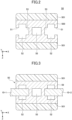
- FIG. 2 is a cross-sectional view of the frame 50 taken along line A-A of FIG. 1 , viewed in the section parallel to the XZ plane.
- the frame 50 includes a conductive main body 500 and slits 51 formed on both sides of the main body 500 in the width direction.
- the slits 51 hold the side edges of the reflection panel 10.
- the side edge of the reflection panel 10 is an edge along the Y direction in FIG. 1 .
- the main body 500 is provided with a cavity 52 communicating with the slit 51, a groove 53 provided in the cavity 52, and a hollow 55 not communicating with the cavity 52 and the groove 53; however, the present invention is not limited to this example.
- the groove 53 is provided at a position facing the slit 51 with the cavity 52 interposed therebetween, and holds the side edge of the reflection panel 10 inserted through the slit 51.
- the weight of the frame 50 can be reduced by providing the cavity 52 and the hollow 55 in the frame 50. Provision of the groove 53 in the cavity 52 reinforces the retention of the reflection panel 10.
- a non-conductive cover 501 such as a resin-made cover, may be provided on the outer surface of the main body 500 but the cover 501 is not essential. In the case where the cover 501 is provided, the cover 501 functions as a protection member that protects the frame 50.
- FIG. 3 is a cross-sectional view parallel to the XZ plane, illustrating the state of insertion of the reflection panel 10 into the frame 50.
- the reflection panels 10-1 and 10-2 are inserted from the slits 51 (see FIG. 2 ) on both sides of the main body 500.
- the reflection panels 10-1 and 10-2 may or may not contact the bottom surface of the groove 53 by being inserted into the groove 53 (see FIG. 2 ) of the cavity 52 to the depth.
- the reflection panels 10-1 and 10-2 are inserted into the slits 51, respectively, so that the neighboring reflection panels 10-1 and 10-2 can be stably held.
- the main body 500 may be partially made of a non-conductive material.
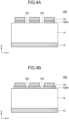
- FIG. 4A, FIG. 4B , and FIG. 4C illustrate examples of the layer structure of the reflection panel 10. These layer structures are a layer structure in the thickness (Z) direction of the reflection panel 10.
- the reflection panel 10A includes a dielectric layer 14, a conductive pattern 151 provided on one of the surfaces of the dielectric layer 14, a ground layer 13 provided on the other of the surfaces of the dielectric layer 14, and an adhesive layer 152A for bonding the conductive pattern 151 to the dielectric layer 14.
- a gap 155 is provided in at least a part of the adhesive layer 152A.
- the dielectric layer 14 is an insulating polymer film such as polycarbonate, cycloolefin polymer (COP), polyethylene terephthalate (PET), or fluorine resin, and has a thickness of about 0.3 mm to 1.0 mm.
- the dielectric layer 14 may be made of any material having a dielectric constant and a dielectric loss tangent suitable for realizing target reflection characteristics, together with the occupancy of the adhesive layer 152A.
- a difference in the occupancy between the conductive pattern 151 and the adhesive layer 152B is 0.0% or more and 40.0% or less, and preferably 0.0% or more and 35.0% or less.
- the difference in the occupancy of 0.0% includes a case where the pattern shapes of the conductive pattern 151 and the adhesive layer 152A coincide with each other within an allowable range of error as in FIG. 4A and a case where the occupancy within the plane is substantially the same on average even when the conductive pattern 151 and the adhesive layer 152 are shifted from each other in places. If a difference in the occupancy between the conductive pattern 151 and the adhesive layer 152B exceeds 40.0%, the occupancy of the adhesive layer 152B becomes too large, and it becomes difficult to suppress the deterioration in reflection efficiency.
- the occupancy of the conductive pattern 151 becomes too small, and it becomes difficult to realize desired reflection characteristics and reflection efficiency.
- the conductive pattern 151 and the adhesive layer 152B are adhered to each other with a difference in the occupancy in the range of 0.0% or more and 40.0% or less.
- the reflection panel 10C includes a dielectric layer 14, a conductive pattern 151 provided on one of the surfaces of the dielectric layer 14, a ground layer 13 provided on the other of the surfaces of the dielectric layer 14, and an adhesive layer 152 for bonding the conductive pattern 151 to the dielectric layer 14.
- the adhesive layer 152 may have substantially the same shape as the conductive pattern 151 like the adhesive layer 152A in FIG. 4A , or may have a planar shape larger than the conductive pattern 151 like the adhesive layer 152B in FIG. 4B .
- the dielectric substrate 17 is preferably made of a material having excellent impact resistance, durability, and transparency.
- the dielectric substrate 17 may be made of polycarbonate, an acrylic resin, PET, or the like.
- the thickness of the intermediate layer 17 is, for example, 1.0 mm to 10.0 mm.
- the conductive pattern 151 covered with the intermediate layer 16 By bonding the conductive pattern 151 covered with the intermediate layer 16 to the dielectric substrate 17, the entry of moisture and air into the surface of the conductive layer 151 is suppressed, and the surface deterioration of the conductive pattern 151 is thereby suppressed.
- the ground layer 13 covered with the intermediate layer 12 By bonding the ground layer 13 covered with the intermediate layer 12 to the dielectric substrate 11, the entry of moisture and air into the surface of the ground layer 13 is suppressed, and the surface deterioration of the ground layer 13 is thereby suppressed. Accordingly, the capacitance between the ground layer 13 and the conductive pattern 151 may be maintained to be constant, and the designed magnitude of a phase delay may be thereby maintained. In other words, the reflection efficiency of the radio waves in the designed direction can be maintained.
- the conductive pattern 151 In a case where the conductive pattern 151 is larger than the adhesive layer 152B, if the difference in the occupancy between the conductive pattern 151 and the adhesive layer 152B exceeds 40.0%, the conductive pattern 151 may be inclined with respect to the XY plane, and it may be difficult to realize the designed reflection characteristics.
- An appropriate occupancy of the conductive pattern 151 can be determined from the viewpoint of maintaining the reflection efficiency of the reflection panel 10 at 60% or more, more preferably 70% or more, and suppressing the deterioration in visible light transmittance.
- the occupancy of the conductive pattern 151 with respect to the dielectric layer 14 is preferably 10.0% or more and 45% or less. If the occupancy of the conductive pattern 151 exceeds 45%, the occupancy of the adhesive layer 152 increases, and there is a possibility that good reflection efficiency cannot be maintained. In addition, the transmittance of the reflection panel 10 is deteriorated. If the occupancy of the conductive pattern 151 is less than 10.0%, it is difficult to realize reflection efficiency of 60% or more.
- an appropriate occupancy of the adhesive layer 152 that can suppress deterioration in reflection efficiency is examined.
- the reflection characteristics are evaluated by changing the occupancy of the adhesive layer of the reflection panel 10 having the above-described layer structure.
- occupancy refers to an area occupancy.
- FIG. 6 is a schematic diagram illustrating the structure of the unit cell 210 of the model 21.
- the unit cell 210 is constituted by six metal patches 211, 212, 213, 214, 215, and 216.
- the width (W) direction and the length (L) direction of the metal patches 211 through 216 correspond to the width (X) direction and the height (Y) direction of the reflection panel 10 of FIG. 1 , respectively.
- the metal patches 211 through 216 have the same width W and different lengths L but have the same central axis of the length (the Y coordinate positions of the central axis are the same).
- the pitch in the X direction is uniform.
- each unit cell 210 is designed in such a manner that the peak of a reflected wave of a normal incidence of an electromagnetic wave (incident angle of 0°) appears in a direction of 50° from the normal.
- FIG. 7 illustrates an example of the arrangement of the conductive patterns 151 on the adhesive layers 152.
- the unit cell 210 of FIG. 6 is constituted on the adhesive layer 152 by a plurality of conductive patterns 151 having different shapes and sizes.
- one unit cell 210 may be constituted on one adhesive layer 152 by arranging a plurality of conductive patterns 151.
- a gap 155 is provided between the adhesive layers 152 so as to partition the unit cells 210.
- the conductive patterns 151 may be arranged in such a manner that two or more unit cells 210 are formed side by side in the Y direction on one adhesive layer 152.
- the conductive patterns 151 may be arranged in such a manner that two or more unit cells 210 are formed side by side in the X direction on one adhesive layer 152.
- the evaluation is conducted in the following manner: a plane wave of 28.0 GHz is made incident at an incident angle of 0°, using the conductive pattern 151 of the model 21 of FIG. 5 , and the scattering cross section of the reflected wave is analyzed by general-purpose three-dimensional electromagnetic field simulation software.
- the scattering cross section namely a radar cross section (RCS), is used as an indicator of the ability to reflect incident electromagnetic waves.
- FIG. 8 illustrates an analysis space 101 of the electromagnetic wave simulation.
- the analysis space is expressed as (a dimension in the X direction) ⁇ (a dimension in the Y direction) ⁇ (a dimension in the Z direction).
- the dimensions of the analysis space 101 are 83.9 mm ⁇ 192.6 mm ⁇ 3.7 mm if the incident electromagnetic wave has a frequency of 28.0 GHz.
- the boundary condition is designed on an assumption that the electromagnetic wave absorber 102 is arranged around the analysis space 101.
- the gain value (a peak value of a reflected waveform) at 50° in the RCS plot in the case where a plane wave of 28.0 GHz incident at an angle of incidence of 0° is reflected at an angle of reflection of 50° is 10.2930 dB.
- the conductive pattern 151 is made of a copper foil having a thickness of 0.05 mm and has the above-described pattern shape.
- the gain value (a peak value of a reflected waveform) at 50° in the RCS plot in the case where a plane wave of 28.0 GHz incident at an angle of incidence of 0° is reflected at an angle of reflection of 50° is 11.4530 dB.
- the conductive pattern 151 is made of a copper foil having a thickness of 0.05 mm and has the above-described pattern shape.
- the gain value (a peak value of a reflected waveform) at 50° in the RCS plot in the case where a plane wave of 28.0 GHz incident at an angle of incidence of 0° is reflected at an angle of reflection of 50° is 11.4940 dB.
- Comparative Example 1 the same layer structure as that of Examples 1 through 5, the adhesive layer 152 having the same thickness as those in Example 1-5 and the same conductive pattern 151 as that of Examples 1 through 5 are used, but the occupancy of the adhesive layer 152 is set to 100%. This corresponds to a configuration in which the entire one surface of the dielectric layer 14 is covered with the adhesive layer 152.
- a polycarbonate film having a thickness of 0.7 mm is used as the dielectric layer 14.
- the ground layer 13 is set on one surface of the polycarbonate film by using an Ag-based multilayer film having a thickness of 0.36 mm.
- the conductive pattern 151 is arranged, with the adhesive layer 152 having a thickness of 0.01 mm and an occupancy of 100.0% interposed therebetween.
- the adhesive layer 152 is an acrylic resin having a relative dielectric constant of 3.01 and a dielectric loss tangent of 0.08 at the frequency of 28.0 GHz.
- the conductive pattern 151 is made of a copper foil having a thickness of 0.05 mm and has the above-described pattern shape.
- the gain value (a peak value of a reflected waveform) at 50° in the RCS plot in the case where a plane wave of 28.0 GHz incident at an angle of incidence of 0° is reflected at an angle of reflection of 50° is 9.9770dB.
- the occupancy of the conductive pattern 151 with respect to the dielectric layer 14 may be set to 10.0% or more and 45% or less in the case where the conductive pattern 151 is 0.01 mm or more and 0.05 mm or less.
- the range of the occupancy of the adhesive layer 152 partially provided on the surface of the dielectric layer 14 also applies to the configuration of FIG. 4C .
- the adhesive layer 152 provided at the occupancy rate of 9.0% or more and 50% or less and the conductive pattern 151 on the adhesive layer 152 may be covered with the intermediate layer 16.
- the intermediate layer 16 By covering the conductive pattern 151 and the adhesive layer 152 with the intermediate layer 16, it is possible to suppress a change in the surface state of the conductive pattern 151 due to the influence of oxygen, moisture, or the like, and weather resistance is therefore improved.
- the electromagnetic wave reflecting device of the embodiment is not limited to the foregoing configuration example.
- the calculation is conducted on the assumption that the acrylic resin having a specific relative dielectric constant and a specific dielectric loss tangent is used as the adhesive layer 152; however, the occupancy of the adhesive layer 152 (9.0% or more and 50.0% or less) is also applicable to a case where a general adhesive having a relative dielectric constant of 2.0 or more and 4.5 or less and a dielectric loss tangent of 0.10 or less is used.
- the range of the occupancy of the adhesive layer 152 is valid over the range of 1 GHz to 28 GHz ⁇ 4 GHz.
- the reflection angle with respect to the normal incidence can be appropriately designed in a range of 35° or more and less than 90° by designing the size, shape, and pitch of the conductive pattern 151 and the dielectric constant of the dielectric layer 14.
- the in-plane size of the reflection panel 10 of the electromagnetic wave reflecting device can be selected as appropriate within a range from 30 cm ⁇ 30 cm to 3 m ⁇ 3 m.
- the entire surface of the reflection panel 10 may be a metasurface, or a part of the reflection panel 10 may be a metasurface and the remaining part may be a specular reflection surface.
- the dielectric substrate may be bonded to the reflective surface after covering the entire surface of the reflective surface with an adhesive film (intermediate layer) having high moisture resistance and durability.
- a gap 155 is provided so that the adhesive layer 152 supporting the conductive pattern 151 is not continuous on the entire surface of the dielectric layer 14.
- the occupancy of the adhesive layer 152 with respect to the dielectric layer 14 may be set to 9.0% or more and 50.0% or less.
- the electromagnetic wave reflecting device 60 and the electromagnetic wave reflecting fence of the embodiment can be installed indoors or outdoors.
Landscapes
- Physics & Mathematics (AREA)
- Electromagnetism (AREA)
- Engineering & Computer Science (AREA)
- Manufacturing & Machinery (AREA)
- Aerials With Secondary Devices (AREA)
- Shielding Devices Or Components To Electric Or Magnetic Fields (AREA)
Applications Claiming Priority (2)
| Application Number | Priority Date | Filing Date | Title |
|---|---|---|---|
| JP2022089849 | 2022-06-01 | ||
| PCT/JP2023/016402 WO2023233879A1 (ja) | 2022-06-01 | 2023-04-26 | 電磁波反射装置、電磁波反射フェンス、及び反射パネル |
Publications (1)
| Publication Number | Publication Date |
|---|---|
| EP4535568A1 true EP4535568A1 (de) | 2025-04-09 |
Family
ID=89026285
Family Applications (1)
| Application Number | Title | Priority Date | Filing Date |
|---|---|---|---|
| EP23815640.0A Pending EP4535568A1 (de) | 2022-06-01 | 2023-04-26 | Elektromagnetische wellen reflektierende vorrichtung, elektromagnetische wellen reflektierender zaun und reflektierende tafel |
Country Status (6)
| Country | Link |
|---|---|
| US (1) | US20250096480A1 (de) |
| EP (1) | EP4535568A1 (de) |
| JP (1) | JPWO2023233879A1 (de) |
| KR (1) | KR20250018469A (de) |
| CN (1) | CN119096428A (de) |
| WO (1) | WO2023233879A1 (de) |
Families Citing this family (1)
| Publication number | Priority date | Publication date | Assignee | Title |
|---|---|---|---|---|
| WO2025229991A1 (ja) * | 2024-04-30 | 2025-11-06 | 大日本印刷株式会社 | 電磁波進行方向制御部材及び導電パターンシート |
Family Cites Families (4)
| Publication number | Priority date | Publication date | Assignee | Title |
|---|---|---|---|---|
| KR101647045B1 (ko) * | 2010-11-08 | 2016-08-10 | 삼성전자주식회사 | 3차원 직립형 메타물질 구조물 및 그 제조방법 |
| JP5832399B2 (ja) | 2011-09-16 | 2015-12-16 | 株式会社半導体エネルギー研究所 | 発光装置 |
| GB201117480D0 (en) * | 2011-10-10 | 2011-11-23 | Palikaras George | Filter |
| EP4131655B1 (de) * | 2020-03-31 | 2025-11-19 | Agc Inc. | Drahtloses übertragungssystem |
-
2023
- 2023-04-26 JP JP2024524246A patent/JPWO2023233879A1/ja active Pending
- 2023-04-26 WO PCT/JP2023/016402 patent/WO2023233879A1/ja not_active Ceased
- 2023-04-26 KR KR1020247034278A patent/KR20250018469A/ko active Pending
- 2023-04-26 EP EP23815640.0A patent/EP4535568A1/de active Pending
- 2023-04-26 CN CN202380036442.9A patent/CN119096428A/zh active Pending
-
2024
- 2024-11-27 US US18/963,018 patent/US20250096480A1/en active Pending
Also Published As
| Publication number | Publication date |
|---|---|
| WO2023233879A1 (ja) | 2023-12-07 |
| CN119096428A (zh) | 2024-12-06 |
| US20250096480A1 (en) | 2025-03-20 |
| JPWO2023233879A1 (de) | 2023-12-07 |
| KR20250018469A (ko) | 2025-02-06 |
Similar Documents
| Publication | Publication Date | Title |
|---|---|---|
| US20250055201A1 (en) | Electromagnetic wave reflecting device, electromagnetic wave reflecting fence, and reflection panel | |
| US12261367B2 (en) | Antenna unit and window glass | |
| US12057631B2 (en) | Antenna unit and window glass | |
| US20250174903A1 (en) | Frequency-selective reflecting plate and communication relay system | |
| US20250096480A1 (en) | Electromagnetic wave reflecting device, electromagnetic wave reflecting fence, and reflection panel | |
| EP4311027A1 (de) | Elektromagnetische wellenreflexionsvorrichtung, elektromagnetische wellenreflexionszaun und verfahren zur montage einer elektromagnetischen wellenreflexionsvorrichtung | |
| EP4518033A1 (de) | Frequenzselektiver reflektor | |
| WO2024127942A1 (ja) | 無線伝達システム | |
| KR20250006862A (ko) | 전자파 반사 장치 및 전자파 반사 펜스 | |
| KR20240144895A (ko) | 전파 반사체 및 건축 재료 | |
| TW202425422A (zh) | 反射板、使用其之電磁波反射裝置及電磁波反射柵 | |
| US20250096479A1 (en) | Electromagnetic wave reflecting device, electromagnetic wave reflecting fence, and reflection panel | |
| WO2024106405A1 (ja) | 電波反射体、電波反射体の作製方法、電波反射構造体、電波反射システムおよび電波反射装置 | |
| WO2023233921A1 (ja) | 電磁波反射装置、電磁波反射フェンス、及び反射パネル | |
| WO2025158773A1 (ja) | 電磁波反射パネル、電磁波反射装置、及び電磁波反射フェンス | |
| US20250309555A1 (en) | Reflection panel and electromagnetic-wave reflecting apparatus | |
| JP2024021078A (ja) | 電波反射体、電波反射体の製造方法および電波反射体の施工方法 | |
| WO2024029365A1 (ja) | 反射パネル、これを用いた電磁波反射装置、及び電磁波反射フェンス | |
| EP4243199A1 (de) | Antennensatz | |
| WO2024241665A1 (ja) | 電磁波反射パネル、電磁波反射装置、及び電磁波反射フェンス | |
| WO2024135216A1 (ja) | 反射パネル、電磁波反射装置、及び電磁波反射フェンス | |
| WO2026058940A1 (ja) | 電波反射体 | |
| JP2026054790A (ja) | 電波反射体および反射鏡アンテナ | |
| WO2024185325A1 (ja) | 電磁波反射パネルの製造方法 | |
| JP2026054789A (ja) | ブラインドおよび電波反射方法 |
Legal Events
| Date | Code | Title | Description |
|---|---|---|---|
| STAA | Information on the status of an ep patent application or granted ep patent |
Free format text: STATUS: THE INTERNATIONAL PUBLICATION HAS BEEN MADE |
|
| PUAI | Public reference made under article 153(3) epc to a published international application that has entered the european phase |
Free format text: ORIGINAL CODE: 0009012 |
|
| STAA | Information on the status of an ep patent application or granted ep patent |
Free format text: STATUS: REQUEST FOR EXAMINATION WAS MADE |
|
| 17P | Request for examination filed |
Effective date: 20241031 |
|
| AK | Designated contracting states |
Kind code of ref document: A1 Designated state(s): AL AT BE BG CH CY CZ DE DK EE ES FI FR GB GR HR HU IE IS IT LI LT LU LV MC ME MK MT NL NO PL PT RO RS SE SI SK SM TR |
|
| DAV | Request for validation of the european patent (deleted) | ||
| DAX | Request for extension of the european patent (deleted) |