EP4535400A1 - Method for controlling surface characteristics and thickness of multilayer transition metal dichalcogenide thin film - Google Patents
Method for controlling surface characteristics and thickness of multilayer transition metal dichalcogenide thin film Download PDFInfo
- Publication number
- EP4535400A1 EP4535400A1 EP23857658.1A EP23857658A EP4535400A1 EP 4535400 A1 EP4535400 A1 EP 4535400A1 EP 23857658 A EP23857658 A EP 23857658A EP 4535400 A1 EP4535400 A1 EP 4535400A1
- Authority
- EP
- European Patent Office
- Prior art keywords
- transition metal
- thin film
- multilayer
- metal dichalcogenide
- amorphous
- Prior art date
- Legal status (The legal status is an assumption and is not a legal conclusion. Google has not performed a legal analysis and makes no representation as to the accuracy of the status listed.)
- Pending
Links
Images


Classifications
-
- H—ELECTRICITY
- H10—SEMICONDUCTOR DEVICES; ELECTRIC SOLID-STATE DEVICES NOT OTHERWISE PROVIDED FOR
- H10P—GENERIC PROCESSES OR APPARATUS FOR THE MANUFACTURE OR TREATMENT OF DEVICES COVERED BY CLASS H10
- H10P14/00—Formation of materials, e.g. in the shape of layers or pillars
- H10P14/20—Formation of materials, e.g. in the shape of layers or pillars of semiconductor materials
- H10P14/34—Deposited materials, e.g. layers
- H10P14/3402—Deposited materials, e.g. layers characterised by the chemical composition
- H10P14/3436—Deposited materials, e.g. layers characterised by the chemical composition being chalcogenide semiconductor materials not being oxides, e.g. ternary compounds
-
- H—ELECTRICITY
- H10—SEMICONDUCTOR DEVICES; ELECTRIC SOLID-STATE DEVICES NOT OTHERWISE PROVIDED FOR
- H10D—INORGANIC ELECTRIC SEMICONDUCTOR DEVICES
- H10D10/00—Bipolar junction transistors [BJT]
- H10D10/80—Heterojunction BJTs
-
- H—ELECTRICITY
- H10—SEMICONDUCTOR DEVICES; ELECTRIC SOLID-STATE DEVICES NOT OTHERWISE PROVIDED FOR
- H10D—INORGANIC ELECTRIC SEMICONDUCTOR DEVICES
- H10D62/00—Semiconductor bodies, or regions thereof, of devices having potential barriers
- H10D62/80—Semiconductor bodies, or regions thereof, of devices having potential barriers characterised by the materials
- H10D62/881—Semiconductor bodies, or regions thereof, of devices having potential barriers characterised by the materials being a two-dimensional material
- H10D62/883—Transition metal dichalcogenides, e.g. MoSe2
-
- H—ELECTRICITY
- H10—SEMICONDUCTOR DEVICES; ELECTRIC SOLID-STATE DEVICES NOT OTHERWISE PROVIDED FOR
- H10P—GENERIC PROCESSES OR APPARATUS FOR THE MANUFACTURE OR TREATMENT OF DEVICES COVERED BY CLASS H10
- H10P14/00—Formation of materials, e.g. in the shape of layers or pillars
- H10P14/20—Formation of materials, e.g. in the shape of layers or pillars of semiconductor materials
- H10P14/29—Formation of materials, e.g. in the shape of layers or pillars of semiconductor materials characterised by the substrates
- H10P14/2901—Materials
- H10P14/2902—Materials being Group IVA materials
- H10P14/2905—Silicon, silicon germanium or germanium
-
- H—ELECTRICITY
- H10—SEMICONDUCTOR DEVICES; ELECTRIC SOLID-STATE DEVICES NOT OTHERWISE PROVIDED FOR
- H10P—GENERIC PROCESSES OR APPARATUS FOR THE MANUFACTURE OR TREATMENT OF DEVICES COVERED BY CLASS H10
- H10P14/00—Formation of materials, e.g. in the shape of layers or pillars
- H10P14/20—Formation of materials, e.g. in the shape of layers or pillars of semiconductor materials
- H10P14/29—Formation of materials, e.g. in the shape of layers or pillars of semiconductor materials characterised by the substrates
- H10P14/2901—Materials
- H10P14/2919—Materials being chalcogenide semiconducting materials not being oxides, e.g. ternary compounds
-
- H—ELECTRICITY
- H10—SEMICONDUCTOR DEVICES; ELECTRIC SOLID-STATE DEVICES NOT OTHERWISE PROVIDED FOR
- H10P—GENERIC PROCESSES OR APPARATUS FOR THE MANUFACTURE OR TREATMENT OF DEVICES COVERED BY CLASS H10
- H10P14/00—Formation of materials, e.g. in the shape of layers or pillars
- H10P14/20—Formation of materials, e.g. in the shape of layers or pillars of semiconductor materials
- H10P14/32—Formation of materials, e.g. in the shape of layers or pillars of semiconductor materials characterised by intermediate layers between substrates and deposited layers
- H10P14/3202—Materials thereof
- H10P14/3236—Materials thereof being chalcogenide semiconducting materials not being oxides, e.g. ternary compounds
-
- H—ELECTRICITY
- H10—SEMICONDUCTOR DEVICES; ELECTRIC SOLID-STATE DEVICES NOT OTHERWISE PROVIDED FOR
- H10P—GENERIC PROCESSES OR APPARATUS FOR THE MANUFACTURE OR TREATMENT OF DEVICES COVERED BY CLASS H10
- H10P14/00—Formation of materials, e.g. in the shape of layers or pillars
- H10P14/20—Formation of materials, e.g. in the shape of layers or pillars of semiconductor materials
- H10P14/34—Deposited materials, e.g. layers
- H10P14/3402—Deposited materials, e.g. layers characterised by the chemical composition
- H10P14/3434—Deposited materials, e.g. layers characterised by the chemical composition being oxide semiconductor materials
-
- H—ELECTRICITY
- H10—SEMICONDUCTOR DEVICES; ELECTRIC SOLID-STATE DEVICES NOT OTHERWISE PROVIDED FOR
- H10P—GENERIC PROCESSES OR APPARATUS FOR THE MANUFACTURE OR TREATMENT OF DEVICES COVERED BY CLASS H10
- H10P14/00—Formation of materials, e.g. in the shape of layers or pillars
- H10P14/20—Formation of materials, e.g. in the shape of layers or pillars of semiconductor materials
- H10P14/34—Deposited materials, e.g. layers
- H10P14/3438—Doping during depositing
- H10P14/3441—Conductivity type
- H10P14/3446—Transition metal elements; Rare earth elements
-
- H—ELECTRICITY
- H10—SEMICONDUCTOR DEVICES; ELECTRIC SOLID-STATE DEVICES NOT OTHERWISE PROVIDED FOR
- H10P—GENERIC PROCESSES OR APPARATUS FOR THE MANUFACTURE OR TREATMENT OF DEVICES COVERED BY CLASS H10
- H10P14/00—Formation of materials, e.g. in the shape of layers or pillars
- H10P14/20—Formation of materials, e.g. in the shape of layers or pillars of semiconductor materials
- H10P14/38—Formation of materials, e.g. in the shape of layers or pillars of semiconductor materials characterised by treatments done after the formation of the materials
-
- H—ELECTRICITY
- H10—SEMICONDUCTOR DEVICES; ELECTRIC SOLID-STATE DEVICES NOT OTHERWISE PROVIDED FOR
- H10P—GENERIC PROCESSES OR APPARATUS FOR THE MANUFACTURE OR TREATMENT OF DEVICES COVERED BY CLASS H10
- H10P50/00—Etching of wafers, substrates or parts of devices
- H10P50/20—Dry etching; Plasma etching; Reactive-ion etching
-
- H—ELECTRICITY
- H10—SEMICONDUCTOR DEVICES; ELECTRIC SOLID-STATE DEVICES NOT OTHERWISE PROVIDED FOR
- H10P—GENERIC PROCESSES OR APPARATUS FOR THE MANUFACTURE OR TREATMENT OF DEVICES COVERED BY CLASS H10
- H10P52/00—Grinding, lapping or polishing of wafers, substrates or parts of devices
-
- H—ELECTRICITY
- H10—SEMICONDUCTOR DEVICES; ELECTRIC SOLID-STATE DEVICES NOT OTHERWISE PROVIDED FOR
- H10P—GENERIC PROCESSES OR APPARATUS FOR THE MANUFACTURE OR TREATMENT OF DEVICES COVERED BY CLASS H10
- H10P95/00—Generic processes or apparatus for manufacture or treatments not covered by the other groups of this subclass
- H10P95/70—Chemical treatments
Definitions
- the present invention relates to methods for controlling the surface properties or characteristics and surface thickness of a multilayer transition metal dichalcogenide thin film, and more specifically, to methods for controlling the surface properties and thickness of a multilayer transition metal dichalcogenide thin film, which may improve the performance of a semiconductor material in a simple and low-cost manner by forming an amorphous transition metal oxide thin film on the multilayer transition metal dichalcogenide thin film, and then treating the multilayer transition metal dichalcogenide thin film, which has the amorphous transition metal oxide thin film formed thereon, at least once with an aqueous ammonium sulfide solution.
- Two-dimensional materials are chemically stable because they have a structure in which strong covalent bonds are formed within a single layer and layers are bonded by relatively weak van der Waals forces.
- TMD transition metal dichalcogenide
- MoSe 2 molybdenum diselenide
- MoS 2 molybdenum disulfide
- MoTe 2 molybdenum ditelluride
- the transition metal dichalcogenide materials have the structure MX 2 (M: a transition metal, X: a chalcogenide), and are materials in which a transition metal from group 4 to group 10 is covalently bonded with two chalcogen atoms. These transition metal dichalcogenides exhibit distinct differences in stability and properties depending on the single-lattice structure, and shows semiconductor properties in the trigonal prismatic structure and metallic properties in the octahedral structure.
- Transition metal dichalcogenides with the above-described properties have attracted great interest in various research fields.
- solution-processable transition metal dichalcogenides have emerged as a new class of materials that are suitable for a wide range of applications in optoelectronics, energy devices, and bio-applications, and exhibit remarkable electrical and catalytic properties, as well as metallic properties.
- transition metal dichalcogenides In order to utilize transition metal dichalcogenides in various application fields, the surface properties and thickness thereof are controlled using heat treatment, plasma, and laser etching techniques. However, these techniques require complex system settings, and therefore, there is a need to develop methods capable of controlling the surface properties and thickness of transition metal dichalcogenides in a simpler and lower-cost manner.
- the technical problem to be solved by the present invention is to provide methods for controlling the surface properties and thickness of a multilayer transition metal dichalcogenide thin film, which may improve the performance of a semiconductor material in a simple and low-cost manner by forming an amorphous transition metal oxide thin film on the multilayer transition metal dichalcogenide thin film, and then treating the multilayer transition metal dichalcogenide thin film, which has the amorphous transition metal oxide thin film formed thereon, at least once with an aqueous ammonium sulfide solution.
- a method for controlling the surface properties of a multilayer transition metal dichalcogenide thin film comprising: step (S10) of forming the multilayer transition metal dichalcogenide thin film on a substrate using a transition metal chalcogenide; step (S20) of forming an amorphous transition metal oxide thin film on the multilayer transition metal dichalcogenide thin film; and step (S30) of treating the multilayer transition metal dichalcogenide thin film, which has the amorphous transition metal oxide thin film formed thereon, with an aqueous ammonium sulfide solution.
- the transition metal chalcogenide may be any one of molybdenum diselenide (MoSe 2 ), molybdenum disulfide (MoS 2 ), and molybdenum ditelluride (MoTe 2 ).
- the transition metal chalcogenide may be molybdenum diselenide (MoSe 2 ).
- the amorphous transition metal oxide thin film may be formed by oxidizing the multilayer transition metal dichalcogenide thin film.
- the amorphous transition metal oxide thin film may be formed by oxidizing the multilayer transition metal dichalcogenide thin film using an oxygen plasma oxidation method.
- the multilayer transition metal dichalcogenide thin film which has the amorphous transition metal oxide thin film formed thereon, may be immersed in the aqueous ammonium sulfide solution.
- a method for controlling the thickness of a multilayer transition metal dichalcogenide thin film comprising: step (S100) of forming the multilayer transition metal dichalcogenide thin film on a substrate using a transition metal chalcogenide; step (S200) of forming an amorphous transition metal oxide thin film on the multilayer transition metal dichalcogenide thin film; step (S300) of subjecting the multilayer transition metal dichalcogenide thin film, which has the amorphous transition metal oxide thin film formed thereon, to a first treatment with an aqueous ammonium sulfide solution; and step (S400) of subjecting the multilayer transition metal dichalcogenide thin film, subjected to the first treatment, to a second treatment with the aqueous ammonium sulfide solution.
- the transition metal chalcogenide may be any one of molybdenum diselenide (MoSe 2 ), molybdenum disulfide (MoS 2 ), and molybdenum ditelluride (MoTe 2 ).
- the transition metal chalcogenide may be molybdenum diselenide (MoSe 2 ).
- the amorphous transition metal oxide thin film may be formed by oxidizing the multilayer transition metal dichalcogenide thin film.
- the amorphous transition metal oxide thin film may be formed by oxidizing the multilayer transition metal dichalcogenide thin film using an oxygen plasma oxidation method.
- the multilayer transition metal dichalcogenide thin film which has the amorphous transition metal oxide thin film formed thereon, may be immersed in the aqueous ammonium sulfide solution.
- step S400 the multilayer transition metal dichalcogenide thin film subjected to the first treatment may be immersed in the aqueous ammonium sulfide solution.
- the time of the second treatment in step S400 may be longer than the time of the first treatment in step S300.
- a transition metal dichalcogenide in a simple and low-cost manner without complex system settings for heat treatment, plasma treatment, laser etching, and the like by forming an amorphous transition metal oxide thin film on a multilayer transition metal dichalcogenide thin film, and then treating the multilayer transition metal dichalcogenide thin film, which has the amorphous transition metal oxide thin film formed thereon, with an aqueous ammonium sulfide solution.
- the present invention when a multilayer transition metal dichalcogenide thin film having an amorphous transition metal oxide thin film formed thereon is to be used as a sensor active layer for detecting risk factors such as hydrogen, it is possible to increase the area for adsorption of the risk factor by controlling the flatness of the surface of the amorphous transition metal oxide thin film and forming nanostructures.
- the present invention may be used to control the specific surface area of the sensor active layer.
- a method for controlling the surface properties of a multilayer transition metal dichalcogenide thin film comprising: step (S10) of forming the multilayer transition metal dichalcogenide thin film on a substrate using a transition metal chalcogenide; step (S20) of forming an amorphous transition metal oxide thin film on the multilayer transition metal dichalcogenide thin film; and step (S30) of treating the multilayer transition metal dichalcogenide thin film, which has the amorphous transition metal oxide thin film formed thereon, with an aqueous ammonium sulfide solution.
- a multilayer transition metal dichalcogenide thin film is formed on a substrate using a transition metal chalcogenide (S10).
- Transition metal chalcogenides are two-dimensional materials that can replace graphene. In principle, they perform only a two-dimensional interaction with constituent atoms. Accordingly, the transport of carriers in transition metal dichalcogenides exhibits a ballistic transport pattern, unlike conventional thin films or bulks, thereby realizing high mobility, high speed, and low power characteristics.
- the transition metal chalcogenide may be any one of molybdenum diselenide (MoSe 2 ), molybdenum disulfide (MoS 2 ), and molybdenum ditelluride (MoTe 2 ), and is preferably molybdenum diselenide (MoSe 2 ).
- MoSe 2 molybdenum diselenide
- MoTe 2 molybdenum ditelluride
- the present invention is not limited thereto, and the transition metal of the transition metal chalcogenide may be replaced with tungsten (W), tin (Sn), rhenium (Re), tantalum (Ta), titanium (Ti), or the like, as long as it is possible to form a volatile chalcogen with a 2H crystal structure.
- a method of forming the multilayer transition metal dichalcogenide thin film on the substrate using the transition metal chalcogenide may be performed using various methods such as a Scotch tape peeling method, a chemical vapor deposition (CVD) method, a physical vapor deposition (PVD) method, a plasma-enhanced chemical vapor deposition (PECVD) method, an atomic layer deposition (ALD) method, and a growth method using a solution (solution process), without being limited thereto.
- CVD chemical vapor deposition
- PVD physical vapor deposition
- PECVD plasma-enhanced chemical vapor deposition
- ALD atomic layer deposition
- the substrate may be a silicon (Si) substrate, but is not limited thereto and various substrates such as a ceramic substrate may be used.
- Amorphous refers to a state in which a solid material has a uniform composition, but the atoms are arranged in a disordered manner, like a liquid, and do not form a regular lattice.
- the amorphous transition metal oxide thin film may be formed by oxidizing the multilayer transition metal dichalcogenide thin film.
- an oxygen plasma method is preferably used in terms of process speed control and homogeneous oxide formation, but is not limited thereto and various oxidation methods such as dry thermal oxidation, wet thermal oxidation, and electrochemical oxidation may be used.
- the diffusion distance that accelerated oxygen atoms can penetrate into a transition metal chalcogenide crystal during oxygen plasma treatment is 3 nm or less, and thus the top surface of the multilayer transition metal dichalcogenide thin film is oxidized, so that the amorphous transition metal oxide thin film and the multilayer transition metal dichalcogenide thin film form a heterojunction structure.
- the transition metal chalcogenide is molybdenum diselenide (MoSe 2 )
- the top surface of the multilayer molybdenum diselenide (MoSe 2 ) thin film is oxidized, so that the molybdenum oxide (MoO x ) thin film and the multilayer molybdenum diselenide (MoSe 2 ) thin film form a MoO x /MoSe 2 heterojunction structure.
- the multilayer transition metal dichalcogenide thin film having the amorphous transition metal oxide thin film formed thereon is treated with an aqueous solution of ammonium sulfide ((NH 4 ) 2 S) (S30).
- a method of treating the multilayer transition metal dichalcogenide thin film having the amorphous transition metal oxide thin film formed thereon with an aqueous solution of ammonium sulfide ((NH 4 ) 2 S) is preferably a method of immersing the multilayer transition metal dichalcogenide thin film having the amorphous transition metal oxide thin film formed thereon in an aqueous solution of ammonium sulfide ((NH 4 ) 2 S) aqueous solution.
- the present invention is not limited thereto, and a method such as spraying may be used if process conditions capable of providing a sufficient reduction reaction within a homogeneous temperature environment are satisfied.
- the multilayer transition metal dichalcogenide thin film having the amorphous transition metal oxide thin film formed thereon is immersed in an aqueous solution of ammonium sulfide ((NH 4 ) 2 S)
- roughness may be imparted to the surface of the multilayer transition metal dichalcogenide thin film during the reduction reaction between ammonium sulfide ((NH 4 )2 S ) and the amorphous transition metal oxide thin film.
- the surface roughness of the multilayer transition metal dichalcogenide thin film is changed, the mobility of charges on the semiconductor surface and the degree of increase in current due to scattering at the surface are changed, whereby the surface properties of the multilayer transition metal dichalcogenide thin film may be controlled in a simple and low-cost manner.
- the degree of surface roughness may be controlled depending on the time period during which the multilayer transition metal dichalcogenide thin film having the amorphous transition metal oxide thin film formed thereon is immersed in an aqueous solution of ammonium sulfide ((NH 4 ) 2 S).
- the time of immersion for controlling the degree of surface roughness is preferably 1 to 600 seconds. If the time of immersion is shorter than 1 second, it is not sufficient to reach the initial reduction reaction, and if the time of immersion is longer than 600 seconds, the amorphous transition metal oxide thin film may be completely etched.
- a method for controlling the thickness of a multilayer transition metal dichalcogenide thin film comprising: step (S100) of forming the multilayer transition metal dichalcogenide thin film on a substrate using a transition metal chalcogenide; step (S200) of forming an amorphous transition metal oxide thin film on the multilayer transition metal dichalcogenide thin film; step (S300) of subjecting the multilayer transition metal dichalcogenide thin film, which has the amorphous transition metal oxide thin film formed thereon, to a first treatment with an aqueous ammonium sulfide solution; and step (S400) of subjecting the multilayer transition metal dichalcogenide thin film, subjected to the first treatment, to a second treatment with the aqueous ammonium sulfide solution.
- a multilayer transition metal dichalcogenide thin film is formed on a substrate using a transition metal chalcogenide (S100).
- transition metal chalcogenide and substrate and the method for forming the multilayer transition metal dichalcogenide thin film on the substrate using the transition metal chalcogenide are identical to those in step S10 of the method for controlling the surface properties of a multilayer transition metal dichalcogenide thin film, and thus detailed description thereof will be omitted for the sake of brevity of the specification.
- step S20 of the method for controlling the surface properties of a multilayer transition metal dichalcogenide thin film are identical to those in step S20 of the method for controlling the surface properties of a multilayer transition metal dichalcogenide thin film, and detailed description thereof will be omitted for the sake of brevity of the specification
- the multilayer transition metal dichalcogenide thin film having the amorphous transition metal oxide thin film formed thereon is subjected to a first treatment with an aqueous ammonium sulfide solution (S300).
- the multilayer transition metal dichalcogenide thin film subjected to the first treatment is subjected to a second treatment with an aqueous ammonium sulfide solution (S400).
- step (S300) of subjecting the multilayer transition metal dichalcogenide thin film having the amorphous transition metal oxide thin film formed thereon to the first treatment with the aqueous ammonium sulfide solution and step (S400) of subjecting the multilayer transition metal dichalcogenide thin film, subjected to the first treatment, to the second treatment with the aqueous ammonium sulfide solution may be performed sequentially.
- the second treatment step (S400) is preferably performed for a longer time than the first treatment step (S300).
- the present invention is not limited thereto, and the multilayer transition metal dichalcogenide thin film subjected to the first treatment may be subjected to an additional cleaning step, and then subjected to the second treatment with the aqueous ammonium sulfide solution.
- the method of subjecting the multilayer transition metal dichalcogenide thin film having the amorphous transition metal oxide thin film formed thereon to the first treatment with the aqueous ammonium sulfide ((NH 4 ) 2 S) solution and the method of subjecting the multilayer transition metal dichalcogenide thin film, subjected to the first treatment, subjected to the second treatment with the aqueous ammonium sulfide ((NH 4 ) 2 S) solution are preferably performed by a method of immersing the thin film in the aqueous ammonium sulfide ((NH 4 ) 2 S) solution.
- the multilayer transition metal dichalcogenide thin film having the amorphous transition metal oxide thin film formed thereon is subjected to a first immersion in the aqueous ammonium sulfide solution, a reduction reaction occurs between the ammonium sulfide and the amorphous transition metal oxide thin film, and the amorphous transition metal oxide thin film is partially or completely removed depending on the time of the first immersion.
- the thin film is subjected to a second immersion in the aqueous ammonium sulfide solution, the thickness of the multilayer transition metal dichalcogenide film is reduced, and the thickness of the multilayer transition metal dichalcogenide film may be controlled depending on the time of the second immersion.
- the amorphous transition metal oxide thin film is partially or completely removed and at the same time, some of the oxygen atoms penetrate into the transition metal dichalcogenide thin film. Then, during the second immersion in the aqueous ammonium sulfide solution, a phenomenon occurs in which the oxygen atoms that have penetrated into the transition metal dichalcogenide thin film react with the ammonium sulfide aqueous solution, decomposing the surrounding transition metal dichalcogenide.
- the thickness of the transition metal dichalcogenide thin film that the oxygen atoms have penetrated is reduced, and the thickness of the multilayer transition metal dichalcogenide thin film may be controlled depending on the time of the second immersion in ammonium sulfide.
- a multilayer molybdenum diselenide (MoSe 2 ) thin film was formed on a 300-nm-thick silicon oxide (SiO 2 ) substrate thermally growth on a p-type silicon (Si) substrate.
- the multilayer molybdenum diselenide (MoSe 2 ) thin film formed on the silicon oxide (SiO 2 ) substrate was treated with oxygen plasma for about 20 minutes using a plasma generator (PDC-32G-2, Harrick plasma Inc.) under the conditions of power of 10.5 W, chamber pressure of 2.33 Torr, and oxygen flow rate of 60 sccm, thereby forming an amorphous molybdenum oxide (MoO x ) layer on the multilayer molybdenum diselenide (MoSe 2 ) thin film.
- a plasma generator PDC-32G-2, Harrick plasma Inc.
- the multilayer molybdenum diselenide (MoSe 2 ) thin film having the amorphous molybdenum oxide (MoO x ) layer formed thereon was immersed in an aqueous ammonium sulfide ((NH 4 ) 2 S) solution (25% concentration) at 323 K for about 10 seconds.
- the bare multilayer molybdenum diselenide (MoSe 2 ) film did not show any noticeable topographic changes ( FIGS. 5(a) and 5(b) ), and the multilayer molybdenum diselenide (MoSe 2 ) thin film after oxygen plasma treatment showed grain features with various diameters (0.12 nm to 0.89 nm) and heights (1 nm to 60 nm) consistent with the development of the amorphous molybdenum oxide (MoO x ) layer on the top layer ( FIGS. 5(c) and 5(d) ).
- the A 1g peak of the bare multilayer molybdenum diselenide (MoSe 2 ) thin film was observed at 239.1 cm -1 ( FIGS. 6(a) and 6(b) ), and the A 1g peak of the multilayer molybdenum diselenide (MoSe 2 ) thin film after oxygen plasma treatment shifted to 241.8 cm -1 , and the peak intensity at around 240 cm -1 decreased by about 70%, indicating that molybdenum diselenide (MoSe 2 ) with a thickness of several nanometers was chemically transferred to the amorphous molybdenum oxide (MoO x ) layer ( FIGS. 6(a) and 6(b) .
- the A 1g peak intensity of the multilayer molybdenum diselenide (MoSe 2 ) thin film after immersion in the aqueous ammonium sulfide solution increased compared to that of the multilayer molybdenum diselenide (MoSe 2 ) thin film after oxygen plasma treatment, but the A 1g peak position remained constant, indicating that the surface properties were changed ( FIGS. 6(a) and 6(b) ).
- the distance between the A 1g peak and the E 1g peak of the multilayer molybdenum diselenide (MoSe 2 ) thin film after ammonium sulfide treatment was about 74.2 cm -1 , which is similar to the distance between the A 1g peak and the E 1g peak of the bare multilayer molybdenum diselenide (MoSe 2 ) thin film, indicating that only the top layer of the initial multilayer molybdenum diselenide (MoSe 2 ) thin film was oxidized by oxygen plasma treatment, so that molybdenum diselenide (MoSe 2 ) existed under the molybdenum oxide (MoO x ) layer ( FIG. 6(c) ).
- a multilayer molybdenum diselenide (MoSe 2 ) thin film was formed on a 300-nm-thick silicon oxide (SiO 2 ) substrate thermally growth on a p-type silicon (Si) substrate.
- the multilayer molybdenum diselenide (MoSe 2 ) thin film formed on the silicon oxide (SiO 2 ) substrate was treated with oxygen plasma for about 20 minutes using a plasma generator (PDC-32G-2, Harrick plasma Inc.) under the conditions of power of 10.5 W, chamber pressure of 2.33 Torr, and oxygen flow rate of 60 sccm, thereby forming an amorphous molybdenum oxide (MoO x ) layer on the multilayer molybdenum diselenide (MoSe 2 ) thin film.
- a plasma generator PDC-32G-2, Harrick plasma Inc.
- the multilayer molybdenum diselenide (MoSe 2 ) thin film having the amorphous molybdenum oxide (MoO x ) layer formed thereon was immersed in an aqueous ammonium sulfide ((NH 4 ) 2 S) solution (25% concentration) at 323 K for about 30 minutes.
- the multilayer molybdenum diselenide (MoSe 2 ) thin film subjected to the first immersion was immersed in an aqueous ammonium sulfide ((NH 4 ) 2 S) solution (25% concentration) at 323 K for about 1 hour.
- an aqueous ammonium sulfide ((NH 4 ) 2 S) solution (25% concentration) at 323 K for about 1 hour.
- AFM images, height profiles extracted from the AFM images, and root mean square (RMS) surface roughnesses of the bare multilayer MoSe 2 thin film, the multilayer MoSe 2 thin film after oxygen plasma treatment, the multilayer MoSe 2 thin film after the first immersion in the aqueous ammonium sulfide solution, and the multilayer MoSe 2 thin film after the second immersion in the aqueous ammonium sulfide solution were measured and compared.
- the thickness of the bare multilayer molybdenum diselenide (MoSe 2 ) thin film was about 88.4 nm, but after oxygen plasma treatment, the thickness of the multilayer molybdenum diselenide (MoSe 2 ) thin film increased to about 92.2 nm, indicating that an amorphous molybdenum oxide (MoO x ) layer with a thickness of about 3.8 nm was formed ( FIGS. 7(a) to 7(d) ).
- the thickness of the multilayer molybdenum diselenide (MoSe 2 ) thin film was reduced to about 86.3 nm, indicating that the amorphous molybdenum oxide (MoO x ) layer was completely removed.
- the thickness of the multilayer molybdenum diselenide (MoSe 2 ) thin film was rapidly reduced to about 38.9 nm, indicating that the thickness of the multilayer molybdenum diselenide (MoSe 2 ) thin film can be controlled depending on the time of the second immersion in the aqueous ammonium sulfide solution ( FIGS. 7(e) to 7(h) ).
Landscapes
- Inorganic Compounds Of Heavy Metals (AREA)
- Chemical & Material Sciences (AREA)
- Crystallography & Structural Chemistry (AREA)
- Inorganic Chemistry (AREA)
- Other Surface Treatments For Metallic Materials (AREA)
- Laminated Bodies (AREA)
Abstract
Description
- The present invention relates to methods for controlling the surface properties or characteristics and surface thickness of a multilayer transition metal dichalcogenide thin film, and more specifically, to methods for controlling the surface properties and thickness of a multilayer transition metal dichalcogenide thin film, which may improve the performance of a semiconductor material in a simple and low-cost manner by forming an amorphous transition metal oxide thin film on the multilayer transition metal dichalcogenide thin film, and then treating the multilayer transition metal dichalcogenide thin film, which has the amorphous transition metal oxide thin film formed thereon, at least once with an aqueous ammonium sulfide solution.
- Two-dimensional materials are chemically stable because they have a structure in which strong covalent bonds are formed within a single layer and layers are bonded by relatively weak van der Waals forces.
- Two-dimensional (2D) transition metal dichalcogenide (TMD) materials, such as molybdenum diselenide (MoSe2), molybdenum disulfide (MoS2), and molybdenum ditelluride (MoTe2), have been widely used in next-generation electronic and optoelectronic devices such as chemical sensors, memory devices, batteries, phototransistors, and photodetectors due to their excellent physical, electronic, and mechanical properties.
- The transition metal dichalcogenide materials have the structure MX2 (M: a transition metal, X: a chalcogenide), and are materials in which a transition metal from
group 4 togroup 10 is covalently bonded with two chalcogen atoms. These transition metal dichalcogenides exhibit distinct differences in stability and properties depending on the single-lattice structure, and shows semiconductor properties in the trigonal prismatic structure and metallic properties in the octahedral structure. - Transition metal dichalcogenides with the above-described properties have attracted great interest in various research fields. In particular, solution-processable transition metal dichalcogenides have emerged as a new class of materials that are suitable for a wide range of applications in optoelectronics, energy devices, and bio-applications, and exhibit remarkable electrical and catalytic properties, as well as metallic properties.
- In order to utilize transition metal dichalcogenides in various application fields, the surface properties and thickness thereof are controlled using heat treatment, plasma, and laser etching techniques. However, these techniques require complex system settings, and therefore, there is a need to develop methods capable of controlling the surface properties and thickness of transition metal dichalcogenides in a simpler and lower-cost manner.
- The technical problem to be solved by the present invention is to provide methods for controlling the surface properties and thickness of a multilayer transition metal dichalcogenide thin film, which may improve the performance of a semiconductor material in a simple and low-cost manner by forming an amorphous transition metal oxide thin film on the multilayer transition metal dichalcogenide thin film, and then treating the multilayer transition metal dichalcogenide thin film, which has the amorphous transition metal oxide thin film formed thereon, at least once with an aqueous ammonium sulfide solution.
- The technical problems of the present invention are not limited to the technical problems mentioned above, and other technical problems not mentioned above will be clearly understood by those skilled in the art from the following description.
- According to one embodiment of the present invention for achieving the technical problem, there is provided a method for controlling the surface properties of a multilayer transition metal dichalcogenide thin film, comprising: step (S10) of forming the multilayer transition metal dichalcogenide thin film on a substrate using a transition metal chalcogenide; step (S20) of forming an amorphous transition metal oxide thin film on the multilayer transition metal dichalcogenide thin film; and step (S30) of treating the multilayer transition metal dichalcogenide thin film, which has the amorphous transition metal oxide thin film formed thereon, with an aqueous ammonium sulfide solution.
- According to one embodiment of the present invention, in step S10, the transition metal chalcogenide may be any one of molybdenum diselenide (MoSe2), molybdenum disulfide (MoS2), and molybdenum ditelluride (MoTe2).
- According to one embodiment of the present invention, the transition metal chalcogenide may be molybdenum diselenide (MoSe2).
- According to one embodiment of the present invention, in step S20, the amorphous transition metal oxide thin film may be formed by oxidizing the multilayer transition metal dichalcogenide thin film.
- According to one embodiment of the present invention, the amorphous transition metal oxide thin film may be formed by oxidizing the multilayer transition metal dichalcogenide thin film using an oxygen plasma oxidation method.
- According to one embodiment of the present invention, in step S30, the multilayer transition metal dichalcogenide thin film, which has the amorphous transition metal oxide thin film formed thereon, may be immersed in the aqueous ammonium sulfide solution.
- According to another embodiment of the present invention for achieving the technical problem, there is provided a method for controlling the thickness of a multilayer transition metal dichalcogenide thin film, comprising: step (S100) of forming the multilayer transition metal dichalcogenide thin film on a substrate using a transition metal chalcogenide; step (S200) of forming an amorphous transition metal oxide thin film on the multilayer transition metal dichalcogenide thin film; step (S300) of subjecting the multilayer transition metal dichalcogenide thin film, which has the amorphous transition metal oxide thin film formed thereon, to a first treatment with an aqueous ammonium sulfide solution; and step (S400) of subjecting the multilayer transition metal dichalcogenide thin film, subjected to the first treatment, to a second treatment with the aqueous ammonium sulfide solution.
- According to another embodiment of the present invention, in step S100, the transition metal chalcogenide may be any one of molybdenum diselenide (MoSe2), molybdenum disulfide (MoS2), and molybdenum ditelluride (MoTe2).
- According to another embodiment of the present invention, the transition metal chalcogenide may be molybdenum diselenide (MoSe2).
- According to another embodiment of the present invention, in step S200, the amorphous transition metal oxide thin film may be formed by oxidizing the multilayer transition metal dichalcogenide thin film.
- According to another embodiment of the present invention, the amorphous transition metal oxide thin film may be formed by oxidizing the multilayer transition metal dichalcogenide thin film using an oxygen plasma oxidation method.
- According to another embodiment of the present invention, in step S300, the multilayer transition metal dichalcogenide thin film, which has the amorphous transition metal oxide thin film formed thereon, may be immersed in the aqueous ammonium sulfide solution.
- According to another embodiment of the present invention, in step S400, the multilayer transition metal dichalcogenide thin film subjected to the first treatment may be immersed in the aqueous ammonium sulfide solution.
- According to another embodiment of the present invention, the time of the second treatment in step S400 may be longer than the time of the first treatment in step S300.
- According to the present invention as described above, it is possible to control the surface properties and thickness of a transition metal dichalcogenide in a simple and low-cost manner without complex system settings for heat treatment, plasma treatment, laser etching, and the like by forming an amorphous transition metal oxide thin film on a multilayer transition metal dichalcogenide thin film, and then treating the multilayer transition metal dichalcogenide thin film, which has the amorphous transition metal oxide thin film formed thereon, with an aqueous ammonium sulfide solution.
- In addition, according to the present invention as described above, when a multilayer transition metal dichalcogenide thin film having an amorphous transition metal oxide thin film formed thereon is to be used as a sensor active layer for detecting risk factors such as hydrogen, it is possible to increase the area for adsorption of the risk factor by controlling the flatness of the surface of the amorphous transition metal oxide thin film and forming nanostructures. Thus, the present invention may be used to control the specific surface area of the sensor active layer.
- In addition, according to the present invention as described above, when a multilayer transition metal dichalcogenide thin film is to be used as a semiconductor element, it is possible to make the thickness of the thin film uniform and control the number of layers, thereby improving the characteristics of the semiconductor element.
- The effects of the present invention are not limited to the effects mentioned above, and other effects not mentioned above will be clearly understood by those skilled in the art from the following description.
-
-
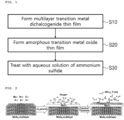
FIG. 1 is a process flow chart showing a method for controlling the surface properties of a multilayer transition metal dichalcogenide thin film according to one embodiment of the present invention. -
FIG. 2 is a schematic view showing a method for controlling the surface properties of a multilayer transition metal dichalcogenide thin film according to one embodiment of the present invention. -
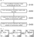
FIG. 3 is a process flow chart showing a method for controlling the thickness of a multilayer transition metal dichalcogenide thin film according to another embodiment of the present invention. -
FIG. 4 shows optical images of Example 1. -
FIG. 5 shows AFM images of Example 1 and graphs showing height profiles extracted from the AFM images. -
FIG. 6(a) is a graph showing the Raman spectra of Example 1,FIG. 5(b) is an enlarged graph of A1g, andFIG. 5(c) is an enlarged graph of E1g. -
FIG. 7 shows AFM images of Example 2 and graphs showing height profiles extracted from the AFM images. - The advantages and features of the present invention, and the way of attaining them, will become apparent with reference to the embodiments described in detail below in conjunction with the accompanying drawings. The present invention may, however, be embodied in different forms and should not be construed as limited to the embodiments disclosed below. Rather, these embodiments are provided so that this disclosure will be thorough and complete, and will fully convey the scope of the present invention to those skilled in the art. The scope of the present invention will be defined by the appended claims. Accordingly, in some embodiments, well-known process steps, well-known device structures and well-known techniques are not described in detail in order to avoid obscuring the present invention. Like reference numerals refer to like elements throughout the specification.
- Terms used in the present specification are for the purpose of describing embodiments and are not intended to limit the present invention. In the present specification, singular forms also include plural expressions unless specified otherwise in the context thereof. As used in the present specification, the terms "comprises" and/or "comprising" specify the presence of stated components, steps, operations and/or elements, but do not preclude the presence or addition of one or more other components, steps, operations and/or elements.
- Identification symbols for individual steps are used for the convenience of explanation. The identification symbols are not intended to describe the operation order of the steps. Therefore, unless otherwise explicitly indicated in the context, the steps may be performed differently from the stated order. In other words, the respective steps may be performed in the same order as the stated order, or performed substantially at the same time, or performed in an order opposite to the stated order.
- Unless otherwise defined, all terms (including technical and scientific terms) used in the present specification have the same meaning as commonly understood by those skilled in the art in the art to which the present invention pertains. In addition, terms, such as those defined in commonly used dictionaries, should not be interpreted as having ideal or excessively formative meanings, unless expressly defined herein.
- According to one preferred embodiment of the present invention, there is provided a method for controlling the surface properties of a multilayer transition metal dichalcogenide thin film, comprising: step (S10) of forming the multilayer transition metal dichalcogenide thin film on a substrate using a transition metal chalcogenide; step (S20) of forming an amorphous transition metal oxide thin film on the multilayer transition metal dichalcogenide thin film; and step (S30) of treating the multilayer transition metal dichalcogenide thin film, which has the amorphous transition metal oxide thin film formed thereon, with an aqueous ammonium sulfide solution.
- Hereinafter, a method for controlling the surface properties of a multilayer transition metal dichalcogenide thin film according to the present invention will be described in detail with reference to a process flow chart shown in
FIG. 1 and a schematic view shown inFIG. 2 . - First, a multilayer transition metal dichalcogenide thin film is formed on a substrate using a transition metal chalcogenide (S10).
- Transition metal chalcogenides are two-dimensional materials that can replace graphene. In principle, they perform only a two-dimensional interaction with constituent atoms. Accordingly, the transport of carriers in transition metal dichalcogenides exhibits a ballistic transport pattern, unlike conventional thin films or bulks, thereby realizing high mobility, high speed, and low power characteristics.
- The transition metal chalcogenide may be any one of molybdenum diselenide (MoSe2), molybdenum disulfide (MoS2), and molybdenum ditelluride (MoTe2), and is preferably molybdenum diselenide (MoSe2). However, the present invention is not limited thereto, and the transition metal of the transition metal chalcogenide may be replaced with tungsten (W), tin (Sn), rhenium (Re), tantalum (Ta), titanium (Ti), or the like, as long as it is possible to form a volatile chalcogen with a 2H crystal structure.
- According to one embodiment of the present invention, a method of forming the multilayer transition metal dichalcogenide thin film on the substrate using the transition metal chalcogenide may be performed using various methods such as a Scotch tape peeling method, a chemical vapor deposition (CVD) method, a physical vapor deposition (PVD) method, a plasma-enhanced chemical vapor deposition (PECVD) method, an atomic layer deposition (ALD) method, and a growth method using a solution (solution process), without being limited thereto.
- The substrate may be a silicon (Si) substrate, but is not limited thereto and various substrates such as a ceramic substrate may be used.
- Next, an amorphous transition metal oxide thin film is formed on the multilayer transition metal dichalcogenide thin film (S20).
- "Amorphous" refers to a state in which a solid material has a uniform composition, but the atoms are arranged in a disordered manner, like a liquid, and do not form a regular lattice.
- According to one embodiment of the present invention, the amorphous transition metal oxide thin film may be formed by oxidizing the multilayer transition metal dichalcogenide thin film. As a method for oxidizing the multilayer transition metal dichalcogenide thin film, an oxygen plasma method is preferably used in terms of process speed control and homogeneous oxide formation, but is not limited thereto and various oxidation methods such as dry thermal oxidation, wet thermal oxidation, and electrochemical oxidation may be used.
- According to one embodiment of the present invention, the diffusion distance that accelerated oxygen atoms can penetrate into a transition metal chalcogenide crystal during oxygen plasma treatment is 3 nm or less, and thus the top surface of the multilayer transition metal dichalcogenide thin film is oxidized, so that the amorphous transition metal oxide thin film and the multilayer transition metal dichalcogenide thin film form a heterojunction structure.
- For example, when the transition metal chalcogenide is molybdenum diselenide (MoSe2), the top surface of the multilayer molybdenum diselenide (MoSe2) thin film is oxidized, so that the molybdenum oxide (MoOx) thin film and the multilayer molybdenum diselenide (MoSe2) thin film form a MoOx/MoSe2 heterojunction structure.
- Finally, the multilayer transition metal dichalcogenide thin film having the amorphous transition metal oxide thin film formed thereon is treated with an aqueous solution of ammonium sulfide ((NH4)2S) (S30).
- According to one embodiment of the present invention, a method of treating the multilayer transition metal dichalcogenide thin film having the amorphous transition metal oxide thin film formed thereon with an aqueous solution of ammonium sulfide ((NH4)2S) is preferably a method of immersing the multilayer transition metal dichalcogenide thin film having the amorphous transition metal oxide thin film formed thereon in an aqueous solution of ammonium sulfide ((NH4)2S) aqueous solution. However, the present invention is not limited thereto, and a method such as spraying may be used if process conditions capable of providing a sufficient reduction reaction within a homogeneous temperature environment are satisfied.
- When the multilayer transition metal dichalcogenide thin film having the amorphous transition metal oxide thin film formed thereon is immersed in an aqueous solution of ammonium sulfide ((NH4)2S), roughness may be imparted to the surface of the multilayer transition metal dichalcogenide thin film during the reduction reaction between ammonium sulfide ((NH4)2S) and the amorphous transition metal oxide thin film. As the surface roughness of the multilayer transition metal dichalcogenide thin film is changed, the mobility of charges on the semiconductor surface and the degree of increase in current due to scattering at the surface are changed, whereby the surface properties of the multilayer transition metal dichalcogenide thin film may be controlled in a simple and low-cost manner.
- According to one embodiment of the present invention, the degree of surface roughness may be controlled depending on the time period during which the multilayer transition metal dichalcogenide thin film having the amorphous transition metal oxide thin film formed thereon is immersed in an aqueous solution of ammonium sulfide ((NH4)2S). The time of immersion for controlling the degree of surface roughness is preferably 1 to 600 seconds. If the time of immersion is shorter than 1 second, it is not sufficient to reach the initial reduction reaction, and if the time of immersion is longer than 600 seconds, the amorphous transition metal oxide thin film may be completely etched.
- According to another preferred embodiment of the present invention, there is provided a method for controlling the thickness of a multilayer transition metal dichalcogenide thin film, comprising: step (S100) of forming the multilayer transition metal dichalcogenide thin film on a substrate using a transition metal chalcogenide; step (S200) of forming an amorphous transition metal oxide thin film on the multilayer transition metal dichalcogenide thin film; step (S300) of subjecting the multilayer transition metal dichalcogenide thin film, which has the amorphous transition metal oxide thin film formed thereon, to a first treatment with an aqueous ammonium sulfide solution; and step (S400) of subjecting the multilayer transition metal dichalcogenide thin film, subjected to the first treatment, to a second treatment with the aqueous ammonium sulfide solution.
- Hereinafter, the method for controlling the thickness of a multilayer transition metal dichalcogenide thin film according to the present invention will be described in detail with reference to the process flow diagram shown in
FIG. 3 . - First, a multilayer transition metal dichalcogenide thin film is formed on a substrate using a transition metal chalcogenide (S100).
- The types of transition metal chalcogenide and substrate and the method for forming the multilayer transition metal dichalcogenide thin film on the substrate using the transition metal chalcogenide are identical to those in step S10 of the method for controlling the surface properties of a multilayer transition metal dichalcogenide thin film, and thus detailed description thereof will be omitted for the sake of brevity of the specification.
- Next, an amorphous transition metal oxide thin film is formed on the multilayer transition metal dichalcogenide thin film (S200).
- The method for forming the amorphous transition metal oxide thin film and the formation of the heterojunction structure by the amorphous transition metal oxide thin film and the multilayer transition metal dichalcogenide thin film are identical to those in step S20 of the method for controlling the surface properties of a multilayer transition metal dichalcogenide thin film, and detailed description thereof will be omitted for the sake of brevity of the specification
- Next, the multilayer transition metal dichalcogenide thin film having the amorphous transition metal oxide thin film formed thereon is subjected to a first treatment with an aqueous ammonium sulfide solution (S300). Finally, the multilayer transition metal dichalcogenide thin film subjected to the first treatment is subjected to a second treatment with an aqueous ammonium sulfide solution (S400).
- According to another embodiment of the present invention, step (S300) of subjecting the multilayer transition metal dichalcogenide thin film having the amorphous transition metal oxide thin film formed thereon to the first treatment with the aqueous ammonium sulfide solution and step (S400) of subjecting the multilayer transition metal dichalcogenide thin film, subjected to the first treatment, to the second treatment with the aqueous ammonium sulfide solution may be performed sequentially. In this case, the second treatment step (S400) is preferably performed for a longer time than the first treatment step (S300). However, the present invention is not limited thereto, and the multilayer transition metal dichalcogenide thin film subjected to the first treatment may be subjected to an additional cleaning step, and then subjected to the second treatment with the aqueous ammonium sulfide solution.
- According to another embodiment of the present invention, the method of subjecting the multilayer transition metal dichalcogenide thin film having the amorphous transition metal oxide thin film formed thereon to the first treatment with the aqueous ammonium sulfide ((NH4)2S) solution and the method of subjecting the multilayer transition metal dichalcogenide thin film, subjected to the first treatment, subjected to the second treatment with the aqueous ammonium sulfide ((NH4)2S) solution are preferably performed by a method of immersing the thin film in the aqueous ammonium sulfide ((NH4)2S) solution.
- When the multilayer transition metal dichalcogenide thin film having the amorphous transition metal oxide thin film formed thereon is subjected to a first immersion in the aqueous ammonium sulfide solution, a reduction reaction occurs between the ammonium sulfide and the amorphous transition metal oxide thin film, and the amorphous transition metal oxide thin film is partially or completely removed depending on the time of the first immersion. Next, when the thin film is subjected to a second immersion in the aqueous ammonium sulfide solution, the thickness of the multilayer transition metal dichalcogenide film is reduced, and the thickness of the multilayer transition metal dichalcogenide film may be controlled depending on the time of the second immersion.
- During the first immersion in the aqueous ammonium sulfide solution, the amorphous transition metal oxide thin film is partially or completely removed and at the same time, some of the oxygen atoms penetrate into the transition metal dichalcogenide thin film. Then, during the second immersion in the aqueous ammonium sulfide solution, a phenomenon occurs in which the oxygen atoms that have penetrated into the transition metal dichalcogenide thin film react with the ammonium sulfide aqueous solution, decomposing the surrounding transition metal dichalcogenide. As a result, the thickness of the transition metal dichalcogenide thin film that the oxygen atoms have penetrated is reduced, and the thickness of the multilayer transition metal dichalcogenide thin film may be controlled depending on the time of the second immersion in ammonium sulfide.
- Hereinafter, examples of the methods for controlling the surface properties and thickness of a multilayer transition metal dichalcogenide thin film according to the present invention will be described. However, it should be understood that these examples are only the most preferred examples of the present invention and do not represent all of the technical spirits of the present invention, and thus there may be various equivalents and modifications capable of replacing them at the time of filing of the present invention.
- Using a Scotch tape method, a multilayer molybdenum diselenide (MoSe2) thin film was formed on a 300-nm-thick silicon oxide (SiO2) substrate thermally growth on a p-type silicon (Si) substrate.
- The multilayer molybdenum diselenide (MoSe2) thin film formed on the silicon oxide (SiO2) substrate was treated with oxygen plasma for about 20 minutes using a plasma generator (PDC-32G-2, Harrick plasma Inc.) under the conditions of power of 10.5 W, chamber pressure of 2.33 Torr, and oxygen flow rate of 60 sccm, thereby forming an amorphous molybdenum oxide (MoOx) layer on the multilayer molybdenum diselenide (MoSe2) thin film.
- The multilayer molybdenum diselenide (MoSe2) thin film having the amorphous molybdenum oxide (MoOx) layer formed thereon was immersed in an aqueous ammonium sulfide ((NH4)2S) solution (25% concentration) at 323 K for about 10 seconds.
- Optical images, AFM images, height profiles extracted from the AFM images, and Raman spectra of the bare multilayer molybdenum diselenide (MoSe2) thin film, the multilayer molybdenum diselenide (MoSe2) thin film after oxygen plasma treatment, and the multilayer molybdenum diselenide (MoSe2) thin film after treatment by immersion in the aqueous ammonium sulfide were measured and compared.
- Referring to
FIG. 4 , it can be seen that the initial morphology was maintained even after the oxidation reaction by oxygen plasma treatment of the multilayer molybdenum diselenide (MoSe2) thin film and the reduction reaction by immersion in the aqueous ammonium sulfide solution, indicating that partial oxidation and reduction on the top layer of the multilayer molybdenum diselenide (MoSe2) thin film were induced. - Referring to
FIG. 5 , the bare multilayer molybdenum diselenide (MoSe2) film did not show any noticeable topographic changes (FIGS. 5(a) and 5(b) ), and the multilayer molybdenum diselenide (MoSe2) thin film after oxygen plasma treatment showed grain features with various diameters (0.12 nm to 0.89 nm) and heights (1 nm to 60 nm) consistent with the development of the amorphous molybdenum oxide (MoOx) layer on the top layer (FIGS. 5(c) and 5(d) ). In addition, in the multilayer molybdenum diselenide (MoSe2) thin film after immersion in the aqueous ammonium sulfide solution, particles having a size of 5 nm or less, such as nanostructures, were uniformly distributed on the surface, indicating that the surface properties were changed (FIGS. 5(e) and 5(f) ). - Referring to
FIG. 6 , the A1g peak of the bare multilayer molybdenum diselenide (MoSe2) thin film was observed at 239.1 cm-1 (FIGS. 6(a) and 6(b) ), and the A1g peak of the multilayer molybdenum diselenide (MoSe2) thin film after oxygen plasma treatment shifted to 241.8 cm-1, and the peak intensity at around 240 cm-1 decreased by about 70%, indicating that molybdenum diselenide (MoSe2) with a thickness of several nanometers was chemically transferred to the amorphous molybdenum oxide (MoOx) layer (FIGS. 6(a) and 6(b) . In addition, the A1g peak intensity of the multilayer molybdenum diselenide (MoSe2) thin film after immersion in the aqueous ammonium sulfide solution increased compared to that of the multilayer molybdenum diselenide (MoSe2) thin film after oxygen plasma treatment, but the A1g peak position remained constant, indicating that the surface properties were changed (FIGS. 6(a) and 6(b) ). - It can be seen that the E1g peaks of the bare multilayer molybdenum diselenide (MoSe2) thin film, the multilayer molybdenum diselenide (MoSe2) thin film after oxygen plasma treatment, and the multilayer molybdenum diselenide (MoSe2) thin film after treatment by immersion in the aqueous ammonium sulfide solution did not change regardless of the oxidation reaction and reduction reaction (
FIG. 6(c) ). In addition, it can be seen that the distance between the A1g peak and the E1g peak of the multilayer molybdenum diselenide (MoSe2) thin film after ammonium sulfide treatment was about 74.2 cm-1, which is similar to the distance between the A1g peak and the E1g peak of the bare multilayer molybdenum diselenide (MoSe2) thin film, indicating that only the top layer of the initial multilayer molybdenum diselenide (MoSe2) thin film was oxidized by oxygen plasma treatment, so that molybdenum diselenide (MoSe2) existed under the molybdenum oxide (MoOx) layer (FIG. 6(c) ). - Using a Scotch tape method, a multilayer molybdenum diselenide (MoSe2) thin film was formed on a 300-nm-thick silicon oxide (SiO2) substrate thermally growth on a p-type silicon (Si) substrate.
- The multilayer molybdenum diselenide (MoSe2) thin film formed on the silicon oxide (SiO2) substrate was treated with oxygen plasma for about 20 minutes using a plasma generator (PDC-32G-2, Harrick plasma Inc.) under the conditions of power of 10.5 W, chamber pressure of 2.33 Torr, and oxygen flow rate of 60 sccm, thereby forming an amorphous molybdenum oxide (MoOx) layer on the multilayer molybdenum diselenide (MoSe2) thin film.
- The multilayer molybdenum diselenide (MoSe2) thin film having the amorphous molybdenum oxide (MoOx) layer formed thereon was immersed in an aqueous ammonium sulfide ((NH4)2S) solution (25% concentration) at 323 K for about 30 minutes.
- The multilayer molybdenum diselenide (MoSe2) thin film subjected to the first immersion was immersed in an aqueous ammonium sulfide ((NH4)2S) solution (25% concentration) at 323 K for about 1 hour.
- AFM images, height profiles extracted from the AFM images, and root mean square (RMS) surface roughnesses of the bare multilayer MoSe2 thin film, the multilayer MoSe2 thin film after oxygen plasma treatment, the multilayer MoSe2 thin film after the first immersion in the aqueous ammonium sulfide solution, and the multilayer MoSe2 thin film after the second immersion in the aqueous ammonium sulfide solution were measured and compared.
- Referring to
FIG. 7 , it can be seen that the thickness of the bare multilayer molybdenum diselenide (MoSe2) thin film was about 88.4 nm, but after oxygen plasma treatment, the thickness of the multilayer molybdenum diselenide (MoSe2) thin film increased to about 92.2 nm, indicating that an amorphous molybdenum oxide (MoOx) layer with a thickness of about 3.8 nm was formed (FIGS. 7(a) to 7(d) ). It can be seen that, after the first immersion in the aqueous ammonium sulfide solution, the thickness of the multilayer molybdenum diselenide (MoSe2) thin film was reduced to about 86.3 nm, indicating that the amorphous molybdenum oxide (MoOx) layer was completely removed. In addition, after the second immersion in the aqueous ammonium sulfide solution, the thickness of the multilayer molybdenum diselenide (MoSe2) thin film was rapidly reduced to about 38.9 nm, indicating that the thickness of the multilayer molybdenum diselenide (MoSe2) thin film can be controlled depending on the time of the second immersion in the aqueous ammonium sulfide solution (FIGS. 7(e) to 7(h) ). - The above-described embodiments of the present invention are merely exemplary, and those skilled in the art will appreciate that the scope of the present invention may include various modifications and equivalents these embodiments.
Claims (14)
- A method for controlling surface properties of a multilayer transition metal dichalcogenide thin film, comprising:step (S10) of forming the multilayer transition metal dichalcogenide thin film on a substrate using a transition metal chalcogenide;step (S20) of forming an amorphous transition metal oxide thin film on the multilayer transition metal dichalcogenide thin film; andstep (S30) of treating the multilayer transition metal dichalcogenide thin film, which has the amorphous transition metal oxide thin film formed thereon, with an aqueous ammonium sulfide solution.
- The method of claim 1, wherein the transition metal chalcogenide in step S10 is any one of molybdenum diselenide (MoSe2), molybdenum disulfide (MoS2), and molybdenum ditelluride (MoTe2).
- The method of claim 2, wherein the transition metal chalcogenide is molybdenum diselenide (MoSe2).
- The method of claim 1, wherein, in step S20, the amorphous transition metal oxide thin film is formed by oxidizing the multilayer transition metal dichalcogenide thin film.
- The method of claim 4, wherein the amorphous transition metal oxide thin film is formed by oxidizing the multilayer transition metal dichalcogenide thin film using an oxygen plasma oxidation method.
- The method of claim 1, wherein, in step S30, the multilayer transition metal dichalcogenide thin film, which has the amorphous transition metal oxide thin film formed thereon, is immersed in the aqueous ammonium sulfide solution.
- A method for controlling a thickness of a multilayer transition metal dichalcogenide thin film, comprising:step (S100) of forming the multilayer transition metal dichalcogenide thin film on a substrate using a transition metal chalcogenide;step (S200) of forming an amorphous transition metal oxide thin film on the multilayer transition metal dichalcogenide thin film;step (S300) of subjecting the multilayer transition metal dichalcogenide thin film, which has the amorphous transition metal oxide thin film formed thereon, to a first treatment with an aqueous ammonium sulfide solution; andstep (S400) of subjecting the multilayer transition metal dichalcogenide thin film, subjected to the first treatment, to a second treatment with the aqueous ammonium sulfide solution.
- The method of claim 7, wherein the transition metal chalcogenide in step S100 is any one of molybdenum diselenide (MoSe2), molybdenum disulfide (MoS2), and molybdenum ditelluride (MoTe2).
- The method of claim 8, wherein the transition metal chalcogenide is molybdenum diselenide (MoSe2).
- The method of claim 7, wherein, in step S200, the amorphous transition metal oxide thin film is formed by oxidizing the multilayer transition metal dichalcogenide thin film.
- The method of claim 10, wherein the amorphous transition metal oxide thin film is formed by oxidizing the multilayer transition metal dichalcogenide thin film using an oxygen plasma oxidation method.
- The method of claim 7, wherein, in step S300, the multilayer transition metal dichalcogenide thin film, which has the amorphous transition metal oxide thin film formed thereon, is immersed in the aqueous ammonium sulfide solution.
- The method of claim 7, wherein, in step S400, the multilayer transition metal dichalcogenide thin film subjected to the first treatment is immersed in the aqueous ammonium sulfide solution.
- The method of claim 7, wherein the time of the second treatment in step S400 is longer than the time of the first treatment in step S300.
Applications Claiming Priority (2)
| Application Number | Priority Date | Filing Date | Title |
|---|---|---|---|
| KR1020220105943A KR102691495B1 (en) | 2022-08-24 | 2022-08-24 | Method for controlling the surface property and thickness of multi-layer transition metal dichalcogenide thin film |
| PCT/KR2023/012271 WO2024043625A1 (en) | 2022-08-24 | 2023-08-18 | Method for controlling surface characteristics and thickness of multilayer transition metal dichalcogenide thin film |
Publications (2)
| Publication Number | Publication Date |
|---|---|
| EP4535400A1 true EP4535400A1 (en) | 2025-04-09 |
| EP4535400A4 EP4535400A4 (en) | 2025-09-24 |
Family
ID=90013529
Family Applications (1)
| Application Number | Title | Priority Date | Filing Date |
|---|---|---|---|
| EP23857658.1A Pending EP4535400A4 (en) | 2022-08-24 | 2023-08-18 | Method for controlling the surface properties and thickness of a multilayer transition metal dichalcogenide thin film |
Country Status (5)
| Country | Link |
|---|---|
| US (1) | US12308231B1 (en) |
| EP (1) | EP4535400A4 (en) |
| JP (1) | JP7788781B2 (en) |
| KR (1) | KR102691495B1 (en) |
| WO (1) | WO2024043625A1 (en) |
Families Citing this family (1)
| Publication number | Priority date | Publication date | Assignee | Title |
|---|---|---|---|---|
| KR102838887B1 (en) * | 2024-04-15 | 2025-07-28 | 경상국립대학교 산학협력단 | An artificial synaptic device comprising transition metal dichalcogenide adsorbed with sulfur hydride molecules and its manufacturing method |
Family Cites Families (12)
| Publication number | Priority date | Publication date | Assignee | Title |
|---|---|---|---|---|
| JPH06232099A (en) * | 1992-09-10 | 1994-08-19 | Mitsubishi Electric Corp | Semiconductor device manufacturing method, semiconductor device manufacturing apparatus, semiconductor laser manufacturing method, quantum wire structure manufacturing method, and crystal growth method |
| JPH11283959A (en) | 1998-03-30 | 1999-10-15 | Hitachi Ltd | Method for manufacturing semiconductor device |
| KR101348059B1 (en) | 2012-07-06 | 2014-01-03 | 성균관대학교산학협력단 | Thin film transistor comprising oxygen plasma treated channel layer and method of manufacturing the same |
| EP2871683B1 (en) | 2013-11-07 | 2021-07-07 | IMEC vzw | Method for cleaning and passivating chalcogenide layers |
| US9245742B2 (en) | 2013-12-18 | 2016-01-26 | Asm Ip Holding B.V. | Sulfur-containing thin films |
| JP6688949B2 (en) | 2015-07-29 | 2020-04-28 | コリア リサーチ インスティチュート オブ スタンダーズ アンド サイエンス | Method for producing two-dimensional transition metal dichalcogenide thin film |
| KR20170056386A (en) | 2015-11-13 | 2017-05-23 | 성균관대학교산학협력단 | Method of manufacturing thin layer of molybdenum disulfide |
| KR101927579B1 (en) * | 2016-02-19 | 2018-12-10 | 경희대학교 산학협력단 | Transition metal dichalcogenide thin film transistor and method of manufacturing the same |
| KR20180002925A (en) | 2016-06-29 | 2018-01-09 | 성균관대학교산학협력단 | Method for controlling the thickness of chalcogenide metal thin film |
| KR102153945B1 (en) * | 2018-12-14 | 2020-09-09 | 한국과학기술원 | Electronic devcie using two dimensional semicondoctor material |
| JP2021169663A (en) | 2020-04-16 | 2021-10-28 | 本田技研工業株式会社 | Growth method of atomic layer ribbons and nanoribbons of transition metal dichalcogenides under moisture control (control) |
| US12480205B2 (en) * | 2020-06-30 | 2025-11-25 | Agency For Science, Technology And Research | Method of growing monolayer transition metal dichalcogenides via sulfurization and subsequent sublimation |
-
2022
- 2022-08-24 KR KR1020220105943A patent/KR102691495B1/en active Active
-
2023
- 2023-08-18 WO PCT/KR2023/012271 patent/WO2024043625A1/en not_active Ceased
- 2023-08-18 US US18/879,209 patent/US12308231B1/en active Active
- 2023-08-18 JP JP2025502632A patent/JP7788781B2/en active Active
- 2023-08-18 EP EP23857658.1A patent/EP4535400A4/en active Pending
Also Published As
| Publication number | Publication date |
|---|---|
| KR20240027999A (en) | 2024-03-05 |
| JP2025527148A (en) | 2025-08-20 |
| KR102691495B1 (en) | 2024-08-05 |
| US12308231B1 (en) | 2025-05-20 |
| WO2024043625A1 (en) | 2024-02-29 |
| EP4535400A4 (en) | 2025-09-24 |
| US20250166992A1 (en) | 2025-05-22 |
| JP7788781B2 (en) | 2025-12-19 |
Similar Documents
| Publication | Publication Date | Title |
|---|---|---|
| Mattinen et al. | Atomic layer deposition of 2D metal dichalcogenides for electronics, catalysis, energy storage, and beyond | |
| EP2899295B1 (en) | Method for producing a thin layer of formula MYx by ALD | |
| Reese et al. | Intrinsic surface passivation of CdTe | |
| JP5259178B2 (en) | Method and apparatus for depositing a thin layer of semiconductor for solar cell manufacture | |
| KR102325522B1 (en) | Method for manufacturing metal chalcogenide film | |
| JP5632359B2 (en) | Method for producing nanostructure on metal oxide substrate, method for depositing thin film on metal oxide substrate, and thin film device | |
| EP3840072B1 (en) | Method for manufacturing a layer of textured aluminium nitride | |
| Park et al. | Tunable electrical properties of vanadium oxide by hydrogen-plasma-treated atomic layer deposition | |
| US12297532B2 (en) | Metal chalcogenide film and method and device for manufacturing the same | |
| KR20210016859A (en) | Method for forming transition metal dichalcogenide film | |
| US12308231B1 (en) | Method for controlling surface characteristics and thickness of multilayer transition metal dichalcogenide thin film | |
| Linevych et al. | Silicon diode structures based on nanowires for temperature sensing application | |
| Rabizadeh et al. | Tuning of physical properties in MoO3 thin films deposited by DC sputtering | |
| Lakhe et al. | Development of CuInTe2 thin film solar cells by electrochemical route with low temperature (80° C) heat treatment procedure | |
| Barnett et al. | XPS investigation of titanium contact formation to ZnO nanowires | |
| Legardinier et al. | Enhancement of the piezoelectric response of ZnO nanowires grown via PLI-MOCVD using post-deposition treatments through adjusted screening and surface effects | |
| Kwon et al. | Artificially controlled two-step electrodeposition of Cu and Cu/In metal precursors with improved surface roughness for solar applications | |
| Ball et al. | Low pressure plasma assisted silicon nanowire growth from self organised tin catalyst particles | |
| Mattinen | Atomic Layer Deposition of Two-Dimensional Metal Dichalcogenides | |
| CN110199052A (en) | The vapor deposition of film comprising gold | |
| Patil et al. | Characterization of silicon films deposited in presence of nitrogen plasma | |
| TWI759950B (en) | Method for making metal compound nanotubes | |
| KR102883211B1 (en) | Method for producing transition metal dichalcogenide with heterojunction structure and transition metal dichalcogenide with heterojunction structure manufactured using the same | |
| Zheng et al. | Low-temperature growth of wafer-scale amorphous boron nitride films with low-dielectric-constant and controllable thicknesses | |
| Sumathi et al. | Investigations on the CdS passivated anodic oxide–InP interface for MOS structures |
Legal Events
| Date | Code | Title | Description |
|---|---|---|---|
| STAA | Information on the status of an ep patent application or granted ep patent |
Free format text: STATUS: THE INTERNATIONAL PUBLICATION HAS BEEN MADE |
|
| PUAI | Public reference made under article 153(3) epc to a published international application that has entered the european phase |
Free format text: ORIGINAL CODE: 0009012 |
|
| STAA | Information on the status of an ep patent application or granted ep patent |
Free format text: STATUS: REQUEST FOR EXAMINATION WAS MADE |
|
| 17P | Request for examination filed |
Effective date: 20250102 |
|
| AK | Designated contracting states |
Kind code of ref document: A1 Designated state(s): AL AT BE BG CH CY CZ DE DK EE ES FI FR GB GR HR HU IE IS IT LI LT LU LV MC ME MK MT NL NO PL PT RO RS SE SI SK SM TR |
|
| REG | Reference to a national code |
Ref country code: DE Ref legal event code: R079 Free format text: PREVIOUS MAIN CLASS: H01L0021020000 Ipc: H01L0021200000 |
|
| A4 | Supplementary search report drawn up and despatched |
Effective date: 20250826 |
|
| RIC1 | Information provided on ipc code assigned before grant |
Ipc: H01L 21/20 20060101AFI20250820BHEP Ipc: H01L 21/02 20060101ALI20250820BHEP |
|
| DAV | Request for validation of the european patent (deleted) | ||
| DAX | Request for extension of the european patent (deleted) |