EP4535398A1 - Semiconductor process device - Google Patents
Semiconductor process device Download PDFInfo
- Publication number
- EP4535398A1 EP4535398A1 EP23814939.7A EP23814939A EP4535398A1 EP 4535398 A1 EP4535398 A1 EP 4535398A1 EP 23814939 A EP23814939 A EP 23814939A EP 4535398 A1 EP4535398 A1 EP 4535398A1
- Authority
- EP
- European Patent Office
- Prior art keywords
- electrode
- assembly
- tubes
- pipe
- protective
- Prior art date
- Legal status (The legal status is an assumption and is not a legal conclusion. Google has not performed a legal analysis and makes no representation as to the accuracy of the status listed.)
- Pending
Links
Images


Classifications
-
- H—ELECTRICITY
- H01—ELECTRIC ELEMENTS
- H01J—ELECTRIC DISCHARGE TUBES OR DISCHARGE LAMPS
- H01J37/00—Discharge tubes with provision for introducing objects or material to be exposed to the discharge, e.g. for the purpose of examination or processing thereof
- H01J37/32—Gas-filled discharge tubes
- H01J37/32431—Constructional details of the reactor
- H01J37/32532—Electrodes
- H01J37/32568—Relative arrangement or disposition of electrodes; moving means
-
- C—CHEMISTRY; METALLURGY
- C23—COATING METALLIC MATERIAL; COATING MATERIAL WITH METALLIC MATERIAL; CHEMICAL SURFACE TREATMENT; DIFFUSION TREATMENT OF METALLIC MATERIAL; COATING BY VACUUM EVAPORATION, BY SPUTTERING, BY ION IMPLANTATION OR BY CHEMICAL VAPOUR DEPOSITION, IN GENERAL; INHIBITING CORROSION OF METALLIC MATERIAL OR INCRUSTATION IN GENERAL
- C23C—COATING METALLIC MATERIAL; COATING MATERIAL WITH METALLIC MATERIAL; SURFACE TREATMENT OF METALLIC MATERIAL BY DIFFUSION INTO THE SURFACE, BY CHEMICAL CONVERSION OR SUBSTITUTION; COATING BY VACUUM EVAPORATION, BY SPUTTERING, BY ION IMPLANTATION OR BY CHEMICAL VAPOUR DEPOSITION, IN GENERAL
- C23C16/00—Chemical coating by decomposition of gaseous compounds, without leaving reaction products of surface material in the coating, i.e. chemical vapour deposition [CVD] processes
- C23C16/44—Chemical coating by decomposition of gaseous compounds, without leaving reaction products of surface material in the coating, i.e. chemical vapour deposition [CVD] processes characterised by the method of coating
- C23C16/455—Chemical coating by decomposition of gaseous compounds, without leaving reaction products of surface material in the coating, i.e. chemical vapour deposition [CVD] processes characterised by the method of coating characterised by the method used for introducing gases into reaction chamber or for modifying gas flows in reaction chamber
- C23C16/45523—Pulsed gas flow or change of composition over time
- C23C16/45525—Atomic layer deposition [ALD]
- C23C16/45527—Atomic layer deposition [ALD] characterized by the ALD cycle, e.g. different flows or temperatures during half-reactions, unusual pulsing sequence, use of precursor mixtures or auxiliary reactants or activations
- C23C16/45536—Use of plasma, radiation or electromagnetic fields
-
- C—CHEMISTRY; METALLURGY
- C23—COATING METALLIC MATERIAL; COATING MATERIAL WITH METALLIC MATERIAL; CHEMICAL SURFACE TREATMENT; DIFFUSION TREATMENT OF METALLIC MATERIAL; COATING BY VACUUM EVAPORATION, BY SPUTTERING, BY ION IMPLANTATION OR BY CHEMICAL VAPOUR DEPOSITION, IN GENERAL; INHIBITING CORROSION OF METALLIC MATERIAL OR INCRUSTATION IN GENERAL
- C23C—COATING METALLIC MATERIAL; COATING MATERIAL WITH METALLIC MATERIAL; SURFACE TREATMENT OF METALLIC MATERIAL BY DIFFUSION INTO THE SURFACE, BY CHEMICAL CONVERSION OR SUBSTITUTION; COATING BY VACUUM EVAPORATION, BY SPUTTERING, BY ION IMPLANTATION OR BY CHEMICAL VAPOUR DEPOSITION, IN GENERAL
- C23C16/00—Chemical coating by decomposition of gaseous compounds, without leaving reaction products of surface material in the coating, i.e. chemical vapour deposition [CVD] processes
- C23C16/44—Chemical coating by decomposition of gaseous compounds, without leaving reaction products of surface material in the coating, i.e. chemical vapour deposition [CVD] processes characterised by the method of coating
- C23C16/455—Chemical coating by decomposition of gaseous compounds, without leaving reaction products of surface material in the coating, i.e. chemical vapour deposition [CVD] processes characterised by the method of coating characterised by the method used for introducing gases into reaction chamber or for modifying gas flows in reaction chamber
- C23C16/45523—Pulsed gas flow or change of composition over time
- C23C16/45525—Atomic layer deposition [ALD]
- C23C16/45544—Atomic layer deposition [ALD] characterized by the apparatus
-
- C—CHEMISTRY; METALLURGY
- C23—COATING METALLIC MATERIAL; COATING MATERIAL WITH METALLIC MATERIAL; CHEMICAL SURFACE TREATMENT; DIFFUSION TREATMENT OF METALLIC MATERIAL; COATING BY VACUUM EVAPORATION, BY SPUTTERING, BY ION IMPLANTATION OR BY CHEMICAL VAPOUR DEPOSITION, IN GENERAL; INHIBITING CORROSION OF METALLIC MATERIAL OR INCRUSTATION IN GENERAL
- C23C—COATING METALLIC MATERIAL; COATING MATERIAL WITH METALLIC MATERIAL; SURFACE TREATMENT OF METALLIC MATERIAL BY DIFFUSION INTO THE SURFACE, BY CHEMICAL CONVERSION OR SUBSTITUTION; COATING BY VACUUM EVAPORATION, BY SPUTTERING, BY ION IMPLANTATION OR BY CHEMICAL VAPOUR DEPOSITION, IN GENERAL
- C23C16/00—Chemical coating by decomposition of gaseous compounds, without leaving reaction products of surface material in the coating, i.e. chemical vapour deposition [CVD] processes
- C23C16/44—Chemical coating by decomposition of gaseous compounds, without leaving reaction products of surface material in the coating, i.e. chemical vapour deposition [CVD] processes characterised by the method of coating
- C23C16/50—Chemical coating by decomposition of gaseous compounds, without leaving reaction products of surface material in the coating, i.e. chemical vapour deposition [CVD] processes characterised by the method of coating using electric discharges
- C23C16/505—Chemical coating by decomposition of gaseous compounds, without leaving reaction products of surface material in the coating, i.e. chemical vapour deposition [CVD] processes characterised by the method of coating using electric discharges using radio frequency discharges
- C23C16/509—Chemical coating by decomposition of gaseous compounds, without leaving reaction products of surface material in the coating, i.e. chemical vapour deposition [CVD] processes characterised by the method of coating using electric discharges using radio frequency discharges using internal electrodes
-
- H—ELECTRICITY
- H01—ELECTRIC ELEMENTS
- H01J—ELECTRIC DISCHARGE TUBES OR DISCHARGE LAMPS
- H01J37/00—Discharge tubes with provision for introducing objects or material to be exposed to the discharge, e.g. for the purpose of examination or processing thereof
- H01J37/32—Gas-filled discharge tubes
- H01J37/32009—Arrangements for generation of plasma specially adapted for examination or treatment of objects, e.g. plasma sources
- H01J37/32082—Radio frequency generated discharge
-
- H—ELECTRICITY
- H01—ELECTRIC ELEMENTS
- H01J—ELECTRIC DISCHARGE TUBES OR DISCHARGE LAMPS
- H01J37/00—Discharge tubes with provision for introducing objects or material to be exposed to the discharge, e.g. for the purpose of examination or processing thereof
- H01J37/32—Gas-filled discharge tubes
- H01J37/32431—Constructional details of the reactor
- H01J37/3244—Gas supply means
-
- H—ELECTRICITY
- H01—ELECTRIC ELEMENTS
- H01J—ELECTRIC DISCHARGE TUBES OR DISCHARGE LAMPS
- H01J37/00—Discharge tubes with provision for introducing objects or material to be exposed to the discharge, e.g. for the purpose of examination or processing thereof
- H01J37/32—Gas-filled discharge tubes
- H01J37/32431—Constructional details of the reactor
- H01J37/32458—Vessel
- H01J37/32513—Sealing means, e.g. sealing between different parts of the vessel
-
- H—ELECTRICITY
- H01—ELECTRIC ELEMENTS
- H01J—ELECTRIC DISCHARGE TUBES OR DISCHARGE LAMPS
- H01J37/00—Discharge tubes with provision for introducing objects or material to be exposed to the discharge, e.g. for the purpose of examination or processing thereof
- H01J37/32—Gas-filled discharge tubes
- H01J37/32431—Constructional details of the reactor
- H01J37/32532—Electrodes
-
- H—ELECTRICITY
- H01—ELECTRIC ELEMENTS
- H01J—ELECTRIC DISCHARGE TUBES OR DISCHARGE LAMPS
- H01J37/00—Discharge tubes with provision for introducing objects or material to be exposed to the discharge, e.g. for the purpose of examination or processing thereof
- H01J37/32—Gas-filled discharge tubes
- H01J37/32431—Constructional details of the reactor
- H01J37/32532—Electrodes
- H01J37/32541—Shape
-
- H—ELECTRICITY
- H01—ELECTRIC ELEMENTS
- H01J—ELECTRIC DISCHARGE TUBES OR DISCHARGE LAMPS
- H01J37/00—Discharge tubes with provision for introducing objects or material to be exposed to the discharge, e.g. for the purpose of examination or processing thereof
- H01J37/32—Gas-filled discharge tubes
- H01J37/32431—Constructional details of the reactor
- H01J37/32532—Electrodes
- H01J37/3255—Material
-
- H—ELECTRICITY
- H01—ELECTRIC ELEMENTS
- H01J—ELECTRIC DISCHARGE TUBES OR DISCHARGE LAMPS
- H01J37/00—Discharge tubes with provision for introducing objects or material to be exposed to the discharge, e.g. for the purpose of examination or processing thereof
- H01J37/32—Gas-filled discharge tubes
- H01J37/32431—Constructional details of the reactor
- H01J37/32532—Electrodes
- H01J37/32559—Protection means, e.g. coatings
-
- H—ELECTRICITY
- H01—ELECTRIC ELEMENTS
- H01J—ELECTRIC DISCHARGE TUBES OR DISCHARGE LAMPS
- H01J37/00—Discharge tubes with provision for introducing objects or material to be exposed to the discharge, e.g. for the purpose of examination or processing thereof
- H01J37/32—Gas-filled discharge tubes
- H01J37/32431—Constructional details of the reactor
- H01J37/32532—Electrodes
- H01J37/32577—Electrical connecting means
-
- H—ELECTRICITY
- H01—ELECTRIC ELEMENTS
- H01J—ELECTRIC DISCHARGE TUBES OR DISCHARGE LAMPS
- H01J37/00—Discharge tubes with provision for introducing objects or material to be exposed to the discharge, e.g. for the purpose of examination or processing thereof
- H01J37/32—Gas-filled discharge tubes
- H01J37/32431—Constructional details of the reactor
- H01J37/32798—Further details of plasma apparatus not provided for in groups H01J37/3244 - H01J37/32788; special provisions for cleaning or maintenance of the apparatus
- H01J37/32816—Pressure
- H01J37/32834—Exhausting
-
- H—ELECTRICITY
- H01—ELECTRIC ELEMENTS
- H01J—ELECTRIC DISCHARGE TUBES OR DISCHARGE LAMPS
- H01J37/00—Discharge tubes with provision for introducing objects or material to be exposed to the discharge, e.g. for the purpose of examination or processing thereof
- H01J37/32—Gas-filled discharge tubes
- H01J37/32431—Constructional details of the reactor
- H01J37/32798—Further details of plasma apparatus not provided for in groups H01J37/3244 - H01J37/32788; special provisions for cleaning or maintenance of the apparatus
- H01J37/32908—Utilities
-
- H—ELECTRICITY
- H10—SEMICONDUCTOR DEVICES; ELECTRIC SOLID-STATE DEVICES NOT OTHERWISE PROVIDED FOR
- H10P—GENERIC PROCESSES OR APPARATUS FOR THE MANUFACTURE OR TREATMENT OF DEVICES COVERED BY CLASS H10
- H10P72/00—Handling or holding of wafers, substrates or devices during manufacture or treatment thereof
- H10P72/04—Apparatus for manufacture or treatment
- H10P72/0402—Apparatus for fluid treatment
-
- H—ELECTRICITY
- H01—ELECTRIC ELEMENTS
- H01J—ELECTRIC DISCHARGE TUBES OR DISCHARGE LAMPS
- H01J2237/00—Discharge tubes exposing object to beam, e.g. for analysis treatment, etching, imaging
- H01J2237/32—Processing objects by plasma generation
- H01J2237/33—Processing objects by plasma generation characterised by the type of processing
- H01J2237/332—Coating
- H01J2237/3321—CVD [Chemical Vapor Deposition]
-
- Y—GENERAL TAGGING OF NEW TECHNOLOGICAL DEVELOPMENTS; GENERAL TAGGING OF CROSS-SECTIONAL TECHNOLOGIES SPANNING OVER SEVERAL SECTIONS OF THE IPC; TECHNICAL SUBJECTS COVERED BY FORMER USPC CROSS-REFERENCE ART COLLECTIONS [XRACs] AND DIGESTS
- Y02—TECHNOLOGIES OR APPLICATIONS FOR MITIGATION OR ADAPTATION AGAINST CLIMATE CHANGE
- Y02P—CLIMATE CHANGE MITIGATION TECHNOLOGIES IN THE PRODUCTION OR PROCESSING OF GOODS
- Y02P70/00—Climate change mitigation technologies in the production process for final industrial or consumer products
- Y02P70/50—Manufacturing or production processes characterised by the final manufactured product
Definitions
- the present disclosure belongs to the field of semiconductor technology, and particularly relates to a semiconductor process device.
- an atomic layer deposition device achieves accurate control of film thickness by adding a precursor into a vacuum chamber during a process cycle period, and can be configured to deposit various films such as a SiO 2 film, a SiNx film, a TiN film, and an A1N film.
- Ionizing a process gas into plasma with a high-frequency electric field is a key technique of a vertical atomic layer deposition device, so that a plasma generation apparatus is one of key structures for ensuring implementation of the process.
- some plasma generation apparatuses adopt an electrode having multiple layers of nickel meshes woven outside, and since a nickel-mesh weaving process is high in cost and requires a large number of nickel materials, the electrode is high in cost and manufacturing difficulty. Meanwhile, a material of the electrode is soft, such that a length of the electrode can be easily changed due to an influence of gravity during the use of the electrode, which affects service life of the electrode.
- An objective of embodiments of the present disclosure is to provide a semiconductor process device capable of solving the above technical problem.
- the present disclosure is implemented as follows.
- the embodiments of the present disclosure provide a semiconductor process device, including: a process pipe and electrode groups;
- the semiconductor process device in the embodiments of the present disclosure adopts the novel electrode assembly, in which the deformable electrode core can be supported and protected by the plurality of electrode tubes, so that an overall strength of the electrode assembly can be improved. Therefore, a length of the electrode assembly is not prone to change under the action of gravity, so that service life of the electrode assembly can be prolonged.
- the electrode assembly in the embodiments of the present disclosure instead of disposing multiple players of nickel meshes outside the electrode core, the plurality of electrode tubes are sequentially nested outside the electrode core along the extension direction of the electrode core, and the electrode mesh is nested outside the plurality of electrode tubes. Such arrangement can reduce the usage amount of nickel meshes, and obviate the need to dispose the multiple layers of nickel meshes, thereby reducing manufacturing cost and manufacturing difficulty of the electrode assembly. Thus, service life of the semiconductor process device can be ensured
- first”, “second” and the like in the description and the claims of the present disclosure are used for distinguishing between similar objects, but not necessarily for describing a particular order or a chronological order. It should be understood that the data such used may be interchanged under appropriate circumstances, so as to allow the embodiments of the present disclosure to be implemented in an order other than those illustrated or described herein; and the objects distinguished by the terms “first”, “second” and the like generally belong to one kind, and the number of the objects is not limited, for example, the number of a first object may be one or more.
- an embodiment of the present disclosure provides a semiconductor process device, which may be a vertical atomic layer deposition device.
- the semiconductor process device may be other devices, which are not particularly limited in the present disclosure.
- the provided semiconductor process device includes a process pipe 200 and electrode groups.
- a process chamber 210 and a buffer chamber 220 are formed inside the process pipe 200, the buffer chamber 220 is communicated with the process chamber 210, and is arranged corresponding to at least one electrode group, one end of each electrode group penetrates through a sidewall of the process chamber 210 and extends into the corresponding buffer chamber 220, and the other end of each electrode group is configured to be connected to a radio frequency power supply.
- Each electrode group includes two electrode assemblies 100, which are configured to be connected to a positive electrode and a negative electrode of the radio frequency power supply, respectively.
- a casing may be welded to the sidewall of the process pipe 200, so as to form the buffer chamber 220 inside the process pipe 200.
- the buffer chamber 220 may be formed at the same time as the process pipe 200 is manufactured.
- the formation method of the buffer chamber 220 is not particularly limited in the embodiments of the present disclosure.
- a process gas in the buffer chamber 220 may be excited into a plasma state, so as to generate plasma, and the plasma enters the process chamber 210 from the buffer chamber 220 to process a wafer in the process chamber 210, during which the radio frequency power supply supplies power to the two electrode assemblies 100 of each electrode group through a radio frequency cable.
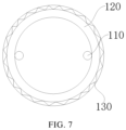
- each electrode assembly 100 includes an electrode core 110, a plurality of electrode tubes 120, and an electrode mesh 130, the plurality of electrode tubes 120 are sequentially arranged along an extension direction of the electrode core 110, a preset gap is provided between every two adjacent electrode tubes 120, the electrode core 110 is inserted into the plurality of electrode tubes 120 and is respectively connected to the plurality of electrode tubes 120, and the electrode mesh 130 is disposed along the extension direction of the electrode core 110 and is nested outside the plurality of electrode tubes 120.
- the strip-shaped electrode assembly 100 is formed by the electrode core 110, the plurality of electrode tubes 120, and the electrode mesh 130 together, so that the electrode assembly 100 may extend into the buffer chamber 220 to generate a high-frequency electric field; and as a result, the process gas introduced into the buffer chamber 220 may be excited to generate the plasma, and the plasma may enter the process chamber 210 from the buffer chamber 220 to achieve a process reaction.
- a length of the electrode tube 120 is in a range of 8mm to 16mm which includes 8mm, 10mm, 12mm, 14mm, 16mm, and the like. Certainly, the length of the electrode tube 120 may be other values. It should be noted here that the electrode tube 120 which is too long is not favorable for installation of the electrode assembly 100, and the electrode tube 120 which is too short may increase processing cost. Therefore, both installation requirements and cost requirements need to be considered in design and manufacturing of the electrode tube 120.
- the electrode core 110 in the embodiments of the present disclosure adopts a soft electrode core, so that the electrode core 110 is deformable and thus can adapt to an installation environment through deformation, so as to reduce installation difficulty of the electrode assembly 100.
- the electrode assembly 100 needs to be endowed with a sufficient strength.
- the plurality of electrode tubes 120 are sequentially nested outside the electrode core 110 along the extension direction of the electrode core 110, so that the plurality of electrode tubes 120 can support and protect the electrode core 110, so as to improve an overall strength of the electrode assembly 100, thereby reducing a change in a length of the electrode assembly 100 during the use of the electrode assembly 100.
- the number of the electrode tubes 120 may be determined according to an overall length of the electrode assembly 100.
- the electrode core 110 is longer, so that more electrode tubes 120 are needed to be nested outside the electrode core 110; and when the electrode assembly 100 needs to be shorter, the electrode core 110 is shorter, so that fewer electrode tubes 120 are needed to be nested outside the electrode core 110.
- the preset gap is provided between every two adjacent electrode tubes 120, leaving certain floating space between the two adjacent electrode tubes 120, so that the electrode assembly 100 can be deformed without causing interference, and overall flexibility of the electrode assembly 100 is ensured.
- the preset gap is in a range of 30mm to 40mm which includes 30mm, 32mm, 35mm, 38mm, 40mm, and the like.
- each electrode tube 120 can improve a local strength of the electrode assembly 100, thereby not only protecting the electrode core 110 but also reducing a change of a length of the electrode core 110.
- the number of buffer chambers 220 may be more than one, a plurality of buffer chambers 220 are distributed along a circumferential direction of the process pipe 200, and are all communicated with the process chamber 210, and each buffer chamber 220 is arranged corresponding to at least one electrode group.
- the process gas can be excited in the plurality of buffer chambers 220 at the same time.
- the plurality of buffer chambers 220 are favorable for improvement in uniformity of the process.
- the method of generating the plasma by respectively exciting the process gas in the plurality of buffer chambers 220 by the plurality of electrode assemblies 100 can reduce power consumption of each electrode assembly 100 under the same process condition, thereby facilitating prolonging the service life of the electrode assembly 100.
- the number of the used buffer chambers 220 may be flexibly adjusted according to different process requirements, so that an increase of energy consumption due to an improper number of the used buffer chambers 220 can be avoided, which can produce the effects of energy conservation and emission reduction to a certain extent.
- the semiconductor process device further includes a plurality of gas intake pipes 600, which penetrate through the sidewall of the process pipe 200 and extend into a plurality of buffer chambers 220 in a one-to-one correspondence manner for introducing the process gas into the corresponding buffer chambers 220, so as to meet demand for the process gas. Since the electrode assemblies 100 may form high-frequency electric fields in the buffer chambers 220, the process gas introduced into each buffer chamber 220 through the gas intake pipes 600 is excited into the plasma state under the action of the high-frequency electric fields to generate the plasma, and the plasma enters the inner chamber of the process pipe 200 from the buffer chambers 220 to participate in the process reaction.
- An exhaust port 230 is provided at the sidewall of the process pipe 200, and is communicated with the process chamber 210 for discharging a gas from the process chamber 210. During each process, a process waste gas generated in the process chamber 210 may be discharged through the exhaust port 230, so as to avoid an excessive gas pressure in the process chamber 210.
- a reaction waste gas is generated in the process chamber 210, and may be discharged through the exhaust port 230, so that the gas pressure in the process chamber 210 can be maintained substantially balanced.
- the exhaust port 230 may be connected to an external vacuum pumping device through an exhaust pipe, so as to discharge the reaction waste gas from the process chamber 210 with the vacuum pumping device.
- a certain vacuum degree may be generated in the process chamber 210 under the action of the vacuum pumping device.
- the semiconductor process device in the embodiments of the present disclosure adopts the novel electrode assembly 100, in which the deformable electrode core 110 is supported and protected by the plurality of electrode tubes 120, so that the overall strength of the electrode assembly 100 can be improved. Therefore, the length of the electrode assembly 100 is not prone to change under the action of gravity, so that the service life of the electrode assembly 100 can be prolonged, so as to prevent the electrode assembly 100 from affecting uniformity of the plasma.
- the plurality of electrode tubes 120 are sequentially nested outside the electrode core 110 along the extension direction of the electrode core 110, and the electrode mesh 130 is nested outside the plurality of electrode tubes 120.
- Such arrangement can reduce the usage amount of the nickel meshes, and obviate the need to dispose the multiple layers of nickel meshes, thereby reducing manufacturing cost and manufacturing difficulty of the electrode assembly 100.
- each electrode assembly 100 may include a plurality of electrode cores 110, each of which is inserted into the plurality of electrode tubes 120 and is fixedly connected to inner walls of the plurality of electrode tubes 120. Based on this, the plurality of electrode tubes 120 can support and protect the electrode cores 110, so as to improve the strength of the electrode assembly 100 while ensuring the overall flexibility of the electrode assembly 100, thereby prolonging the service life of the electrode assembly 100. Moreover, all the plurality of electrode cores 110 are respectively connected to the inner wall of each electrode tube 120, so that every two adjacent electrode tubes 120 can be connected to each other firmly and stably, so as to ensure the service life of the electrode assembly 100.
- the electrode cores 110 may be fixed to the inner walls of the electrode tubes 120 by welding or bonding, so that firmness of the connection of the electrode cores 110 to the inner walls of the electrode tubes 120 can be improved, which can prolong the service life of the electrode assembly 100.
- the electrode assembly 100 may include two electrode cores 110, which are fixedly connected to two opposite sides of the inner walls of the electrode tubes 120, respectively. In this way, the two opposite sides of the inner wall of each electrode tube 120 can be fixedly connected so make a force applied to each electrode tube 120 more uniform, so that stability of the connection of every two adjacent electrode tubes 120 can be ensured.
- the electrode cores 110 included in the electrode assembly 100 may be in other numbers, and the number of the electrode cores 110 is not particularly limited in the embodiments of the present disclosure.
- the electrode core 110 may be a nickel wire which has a small diameter and is soft, so as to enable the electrode assembly 100 to be freely deformed.
- the electrode core 110 may be made of other materials and into other shapes, and the material and the shape of the electrode core 110 are not particularly limited in the embodiments of the present disclosure.
- the electrode tube 120 may be a nickel tube which has a diameter larger than that of the nickel wire and is harder, so as to support and protect the electrode core 110 inserted in the electrode tube 120, thereby alleviating the problem that the service life is affected by the change of the length of the electrode core 110 due to deformation.
- the electrode tube 120 may be made of other materials, and the material of the electrode tube 120 is not particularly limited in the embodiments of the present disclosure.
- the electrode mesh 130 may be a nickel mesh. Under the condition of the same overall dimension of the electrode assembly 100, compared with the method of weaving multiple layers of nickel meshes outside the electrode core 110, the method of disposing the electrode tubes 120 outside the electrode core 110 and nesting the electrode mesh 130 outside the electrode tubes 120 obviates the need to weave the multiple layers of nickel meshes, and just needs a thin nickel mesh layer such as one layer of nickel mesh, so that the usage amount of nickel can be reduced, which can reduce the manufacturing cost and the manufacturing difficulty.
- the electrode mesh 130 may be made of other materials, and the material of the electrode mesh 130 is not particularly limited in the embodiments of the present disclosure.
- two buffer chambers 220 are formed inside the process pipe 200, and are symmetrically arranged on two sides of the exhaust port 230. Based on this, the electrode assemblies 100 respectively excite the process gas into the plasma state in the two buffer chambers 220 to generate the plasma, and the plasma flows into the process chamber 210 from the two buffer chambers 220, which can improve the uniformity of the plasma in the process chamber 210 to improve film quality of a process product.
- more buffer chambers 220 may be disposed along the circumferential direction of the process pipe 200 and symmetrically distributed on the two sides of the exhaust port 230. In this way, by increasing the number of the buffer chambers 220 and equally distributing the plurality of buffer chambers 220 around the process chamber 210, a more uniform plasma atmosphere can be easily formed in the process chamber 210, thereby further improving uniformity of film thickness.
- a plurality of through holes are provided on a side of each buffer chamber 220 away from the process pipe 200, and are arranged along an axial direction of the process pipe 200 for connecting the buffer chamber 220 to the process chamber 210. Based on this, a flow area of the process gas in the axial direction of the process pipe 200 can be increased, so that the process gas can be distributed more uniformly in the process chamber 210, so as to improve the film quality of the process product.
- the semiconductor process device may further include a protective pipe group, which includes at least one protective pipe 300, the protective pipe 300 penetrates through the sidewall of the process pipe and extends into the buffer chamber 220, and at least one electrode assembly 100 of the electrode group is inserted into the protective pipe 300.
- a protective pipe group which includes at least one protective pipe 300, the protective pipe 300 penetrates through the sidewall of the process pipe and extends into the buffer chamber 220, and at least one electrode assembly 100 of the electrode group is inserted into the protective pipe 300.
- the number of protective pipe groups is the same as the number of the electrode groups, and the protective pipe groups and the electrode groups are arranged in a one-to-one correspondence manner.
- the electrode assembly 100 can be mounted and guided through the protective pipe 300, so as to allow an end of the electrode assembly 100 to extend into the buffer chamber 220; and on the other hand, the protective pipe 300 can prevent contaminants from entering the process chamber 210 and protect the electrode assembly 100.
- the protective pipe 300 may be a quartz pipe.
- the protective pipe 300 may be fixed to the process pipe 200 by welding, bonding, clamping, or screwing, so as to ensure firmness and stability of the connection of the protective pipe 300 and the process pipe 200.
- one protective pipe group may include two protective pipes 300, and two electrode assemblies 100 of one electrode group are respectively inserted into the two protective pipes 300, and two electrode assemblies 100 of a same electrode group are respectively connected to the positive electrode and the negative electrode of the radio frequency power supply. Based on this, the two electrode assemblies 100 of each electrode group can be mounted and protected with two protective pipes 300, respectively.
- lengths of the two electrode assemblies 100 of each electrode group in the two protective pipes 300 are kept the same as much as possible, so as to ensure uniformity of generated electric fields.
- lengths of cables for connecting the two electrode assemblies 100 to the radio frequency power supply are kept the same as much as possible, so as to ensure consistency of phases of the two electric fields respectively generated by the two electrode assemblies 100.
- the semiconductor process device may further include a first connecting assembly 400 and a second connecting assembly 500, which are provided for each electrode assembly 100.
- the first connecting assembly 400 is nested outside the protective pipe 300 and the second connecting assembly 500, and is respectively hermetically connected to the protective pipe 300 and the second connecting assembly 500, one end of the second connecting assembly 500 is connected to the electrode assembly 100, and the other end of the second connecting assembly 500 is configured to be connected to the radio frequency power supply.
- the electrode assembly 100 can be mounted to and sealed with the protective pipe 300; and with the second connecting assembly 500, the electrode assembly 100 can be electrically connected to a radio frequency cable, and sealed with the first connecting assembly 400, so as to protect a joint of the second connecting assembly 500 and the electrode assembly 100, and avoid oxidation of the electrode assembly 100.
- the semiconductor process device may further include a supporting block 700, which is fixed to a water-cooled pressure ring (not shown) of the semiconductor process device with a screw, and has a top butted to the first connecting assembly 400, so as to support the first connecting assembly 400.
- a supporting block 700 which is fixed to a water-cooled pressure ring (not shown) of the semiconductor process device with a screw, and has a top butted to the first connecting assembly 400, so as to support the first connecting assembly 400.
- the first connecting assembly 400 may include an electrode holder 410, a first locking member 420, and a second locking member 430.
- the electrode holder 410 is provided with a through cavity 411, one end of the electrode assembly 100 is disposed in the through cavity 411, at least part of the second connecting assembly 500 is disposed in the through cavity 411 and is connected to the electrode assembly 100, the electrode holder 410 is connected to the protective pipe 300 through the first locking member 420, and the second connecting assembly 500 is hermetically connected to the electrode holder 410 through the second locking member 430. Based on this, the assembly of the first connecting assembly 400 and the second connecting assembly 500 can be realized, and tightness of the assembly of the first connecting assembly 400 and the second connecting assembly 500 can be ensured.
- the first locking member 420 may be disposed at an end of the protective pipe 300 away from the process pipe 200.
- the first connecting assembly 400 may be mounted to the protective pipe 300.
- the first locking member 420 may be provided with an avoidance hole.
- the first locking member 420 may be regarded as a nut, and is nested outside an outer wall of the protective pipe 300 through the avoidance hole, and fixedly connected to the protective pipe 300; certainly, the first locking member 420 may be movably nested outside the protective pipe 300, and a blocking part may be provided outside the protective pipe 300 to prevent the first locking member 420 from being detached from the protective pipe 300. Based on this, installation stability of the first connection member 400 and the protective pipe 300 can be secured.
- the first locking member 420 may be connected to one end of the electrode holder 410 by threads, so that the first connecting assembly 400 may be detachably mounted to the protective pipe 300, so as to facilitate detaching the electrode holder 410, thereby facilitating replacement or maintenance of the electrode assembly 100.
- the electrode holder 410 may be detached together with the electrode assembly 100, so as to facilitate the replacement or the maintenance of the electrode assembly 100.
- the second locking member 430 is provided with an avoidance hole, so as to allow the other end of the second connecting assembly 500 to extend out of the through cavity 411, thereby facilitating the connection of the second connecting assembly 500 to the external radio frequency cable.
- the second locking member 430 may be connected to the other end of the electrode holder 410 by threads, and may be regarded as a nut, which can facilitate detachment. Based on this, when the second connecting assembly 500 does not need to be detached, the second locking member 430 is fastened to the other end of the electrode holder 410, and in this case, the second connecting assembly 500 may be firmly fixed to the electrode holder 410 through the second locking member 430, so as to prevent the second connecting assembly 500 from being detached from the electrode assembly 100 to affect energy transmission; and when the second connecting assembly 500 needs to be detached, just by detaching the second locking member 430 from the electrode holder 410 to remove the limiting effect on the second connecting assembly 500, the second connecting assembly 500 may be detached. In this way, the detachment of the second connecting assembly 500 is facilitated, which improves replacement efficiency or maintenance efficiency of the second connecting assembly 500.
- the electrode holder 410 can protect the joint of the electrode assembly 100 and the second connecting assembly 500 against interference from external factors.
- the semiconductor process device may further include a protective gas pipeline (not shown), a protective gas inlet 450 is provided at a sidewall of the through cavity 411, two protective pipes 300 of a same protective pipe group are hermetically communicated with each other in the corresponding buffer chamber 220, and the protective gas pipeline is communicated with an interior of the protective pipe 300 through the protective gas inlet 450 for introducing a protective gas.
- a protective gas pipeline (not shown)
- a protective gas inlet 450 is provided at a sidewall of the through cavity 411
- two protective pipes 300 of a same protective pipe group are hermetically communicated with each other in the corresponding buffer chamber 220
- the protective gas pipeline is communicated with an interior of the protective pipe 300 through the protective gas inlet 450 for introducing a protective gas.
- an external protective gas i.e., an anti-oxidation gas
- an external protective gas i.e., an anti-oxidation gas
- an anti-oxidation gas may be introduced into the through cavity 411 through the protective gas inlet 450, flow into the buffer chamber 220 through one of the two protective pipes 300, and is discharged through the other of the two protective pipes 300.
- an external protective gas i.e., an anti-oxidation gas
- the second connecting assembly 500 may include an electrode terminal 510 and a fastener 520.
- a first connecting end 511 of the electrode terminal 510 which is located in the through cavity 411 is provided with a first mounting hole
- a second connecting end 140 of the electrode assembly 100 which is located in the through cavity 411 is provided with a second mounting hole.
- the first connecting end 511 and the second connecting end 140 overlap each other, and the fastener 520 is inserted into the first mounting hole and the second mounting hole in sequence to fasten the first connecting end 511 to the second connecting end 140.
- the second connecting assembly 500 may further include a gasket 530, which is provided with a third mounting hole, and is disposed on a side of the second connecting end 140 away from the first connecting end 511.
- the first mounting hole, the second mounting hole, and the third mounting hole are arranged coaxially, the fastener 520 is inserted into the first mounting hole, the second mounting hole, and the third mounting hole, and the second connecting end 140 is pressed against the first connecting end 511 through the gasket 530, so that the second connecting end 140 and the first connecting end 511 are pressed against each other, thereby ensuring good contact between the first connecting end 511 and the second connecting end 140, and avoiding a virtual connection.
- each of the first connecting end 511 and the second connecting end 140 may be a flat structure, so as to increase a contact area between the first connecting end 511 and the second connecting end 140, thereby further improving the stability of the connection.
- a first sealing member 440 may be provided between the first locking member 420 and the electrode holder 410 to seal a gap between the first locking member 420 and the electrode holder 410.
- a second sealing member 440' may be provided between the second locking member 430 and the electrode holder 410 to seal a gap between the second locking member 430 and the electrode holder 410.
- the through cavity 411 can be sealed under the condition that the first locking member 420 is fastened to the electrode holder 410 and the second locking member 430 is fastened to the electrode holder 410, so that external impurities and the like can be prevented from entering the through cavity 411 to affect the joint of the electrode assembly 100 and the second connecting assembly 500, which ensures the stability and reliability of the connection of the electrode assembly 100 and the second connecting assembly 500.
- first sealing member 440 and the second sealing member 440' may be both seal rings, which are respectively nested outside two ends of the electrode holder 410, so as to allow the electrode assembly 100 and the second connecting member 500 to extend out of the through cavity 411.
- a working principle of the semiconductor process device is as follows: the external radio frequency power supply transmits energy to the electrode assembly 100 through the radio frequency cable, so as to enable the electrode assembly 100 to generate the high-frequency electric field in the buffer chamber 220; and the process gas is introduced into the buffer chamber 220 through a process gas pipeline and the gas intake piped 600 in sequence, and is excited into the plasma state by the high-frequency electric field in the buffer chamber 220 to generate the plasma, and the plasma enters the process chamber 210 from the buffer chamber 220 to participate in the reaction, thereby realizing the process.
- the usage amount of a high-value material e.g., nickel
- the strength of the electrode assembly 100 can be improved while ensuring overall flexibility of the electrode assembly 100, so that the service life of the electrode assembly 100 can be prolonged, and the reliability of the electrode assembly 100 can be improved.
- the uniformity of the plasma in the process chamber 210 can be improved, so as to improve process performance and ensure the uniformity of the film thickness.
Landscapes
- Chemical & Material Sciences (AREA)
- Engineering & Computer Science (AREA)
- Physics & Mathematics (AREA)
- Plasma & Fusion (AREA)
- Analytical Chemistry (AREA)
- General Chemical & Material Sciences (AREA)
- Chemical Kinetics & Catalysis (AREA)
- Materials Engineering (AREA)
- Mechanical Engineering (AREA)
- Metallurgy (AREA)
- Organic Chemistry (AREA)
- Electromagnetism (AREA)
- Plasma Technology (AREA)
Abstract
Description
- The present disclosure belongs to the field of semiconductor technology, and particularly relates to a semiconductor process device.
- Adopting a radio frequency mode, an atomic layer deposition device achieves accurate control of film thickness by adding a precursor into a vacuum chamber during a process cycle period, and can be configured to deposit various films such as a SiO2 film, a SiNx film, a TiN film, and an A1N film. Ionizing a process gas into plasma with a high-frequency electric field is a key technique of a vertical atomic layer deposition device, so that a plasma generation apparatus is one of key structures for ensuring implementation of the process.
- At present, some plasma generation apparatuses adopt an electrode having multiple layers of nickel meshes woven outside, and since a nickel-mesh weaving process is high in cost and requires a large number of nickel materials, the electrode is high in cost and manufacturing difficulty. Meanwhile, a material of the electrode is soft, such that a length of the electrode can be easily changed due to an influence of gravity during the use of the electrode, which affects service life of the electrode.
- An objective of embodiments of the present disclosure is to provide a semiconductor process device capable of solving the above technical problem.
- In order to solve the above technical problem, the present disclosure is implemented as follows.
- The embodiments of the present disclosure provide a semiconductor process device, including: a process pipe and electrode groups;
- a process chamber and a buffer chamber are formed inside the process pipe, the buffer chamber is communicated with the process chamber and arranged corresponding to at least one of the electrode groups, one end of each of the electrode groups penetrates through a sidewall of the process chamber and extends into the buffer chamber, and the other end of each of the electrode groups is configured to be connected to a radio frequency power supply, wherein
- each of the electrode groups includes two electrode assemblies, which are configured to be connected to a positive electrode and a negative electrode of the radio frequency power supply, respectively; each of the electrode assemblies includes a deformable electrode core, a plurality of electrode tubes, and an electrode mesh, the plurality of electrode tubes are sequentially arranged along an extension direction of the electrode core, a preset gap is provided between every two adjacent electrode tubes, and the electrode core is inserted into the plurality of electrode tubes, and is respectively connected to the plurality of electrode tubes; and the electrode mesh is disposed along the extension direction of the electrode core, and is nested outside the plurality of electrode tubes.
- Compared with some existing plasma generation apparatuses adopting the electrode having the multiple layers of nickel meshes woven outside, the semiconductor process device in the embodiments of the present disclosure adopts the novel electrode assembly, in which the deformable electrode core can be supported and protected by the plurality of electrode tubes, so that an overall strength of the electrode assembly can be improved. Therefore, a length of the electrode assembly is not prone to change under the action of gravity, so that service life of the electrode assembly can be prolonged. Meanwhile, for the electrode assembly in the embodiments of the present disclosure, instead of disposing multiple players of nickel meshes outside the electrode core, the plurality of electrode tubes are sequentially nested outside the electrode core along the extension direction of the electrode core, and the electrode mesh is nested outside the plurality of electrode tubes. Such arrangement can reduce the usage amount of nickel meshes, and obviate the need to dispose the multiple layers of nickel meshes, thereby reducing manufacturing cost and manufacturing difficulty of the electrode assembly. Thus, service life of the semiconductor process device can be ensured
-
-
FIG. 1 is a first schematic structural diagram of a semiconductor process device according to an embodiment of the present disclosure; -
FIG. 2 is a second schematic structural diagram of a semiconductor process device according to an embodiment of the present disclosure; -
FIG. 3 is a schematic structural diagram of a process pipe, a protective pipe, and a gas intake pipe according to an embodiment of the present disclosure; -
FIG. 4 is a partial view of a process pipe, a protective pipe, a gas intake pipe, an electrode assembly, a first connecting assembly, and a second connecting assembly according to an embodiment of the present disclosure; -
FIG. 5 is a partial view of an electrode assembly, a first connecting assembly, and a second connecting assembly according to an embodiment of the present disclosure; -
FIG. 6 is a first schematic diagram of an electrode assembly according to an embodiment of the present disclosure; and -
Fig. 7 is a second schematic diagram of an electrode assembly according to an embodiment of the present disclosure. - The technical solutions provided in the embodiments of the present disclosure are clearly and thoroughly described below with reference to the drawings for the embodiments of the present disclosure. Apparently, the embodiments described herein are just some embodiments of the present disclosure, and do not cover all embodiments. All other embodiments derived by those of ordinary skill in the art from the embodiments described herein without inventive work fall within the scope of the present disclosure.
- The terms "first", "second" and the like in the description and the claims of the present disclosure are used for distinguishing between similar objects, but not necessarily for describing a particular order or a chronological order. It should be understood that the data such used may be interchanged under appropriate circumstances, so as to allow the embodiments of the present disclosure to be implemented in an order other than those illustrated or described herein; and the objects distinguished by the terms "first", "second" and the like generally belong to one kind, and the number of the objects is not limited, for example, the number of a first object may be one or more. In addition, the term "and/or" in the description and the claims indicates at least one of the objects connected by the term "and/or", and the forward slash "/" generally indicates that the object before "/" and the object after "/" are in an "or" relationship.
- With reference to the drawings, the embodiments of the present disclosure are described in detail below in conjunction with specific embodiments and application scenarios.
- Referring to
FIG. 1 to FIG. 7 , an embodiment of the present disclosure provides a semiconductor process device, which may be a vertical atomic layer deposition device. Certainly, the semiconductor process device may be other devices, which are not particularly limited in the present disclosure. The provided semiconductor process device includes aprocess pipe 200 and electrode groups. Aprocess chamber 210 and abuffer chamber 220 are formed inside theprocess pipe 200, thebuffer chamber 220 is communicated with theprocess chamber 210, and is arranged corresponding to at least one electrode group, one end of each electrode group penetrates through a sidewall of theprocess chamber 210 and extends into thecorresponding buffer chamber 220, and the other end of each electrode group is configured to be connected to a radio frequency power supply. Each electrode group includes twoelectrode assemblies 100, which are configured to be connected to a positive electrode and a negative electrode of the radio frequency power supply, respectively. - Optionally, a casing may be welded to the sidewall of the
process pipe 200, so as to form thebuffer chamber 220 inside theprocess pipe 200. Or, thebuffer chamber 220 may be formed at the same time as theprocess pipe 200 is manufactured. The formation method of thebuffer chamber 220 is not particularly limited in the embodiments of the present disclosure. - By providing the
electrode assembly 100, a process gas in thebuffer chamber 220 may be excited into a plasma state, so as to generate plasma, and the plasma enters theprocess chamber 210 from thebuffer chamber 220 to process a wafer in theprocess chamber 210, during which the radio frequency power supply supplies power to the two electrode assemblies 100 of each electrode group through a radio frequency cable. - As shown in
FIG. 6 , eachelectrode assembly 100 includes anelectrode core 110, a plurality ofelectrode tubes 120, and anelectrode mesh 130, the plurality ofelectrode tubes 120 are sequentially arranged along an extension direction of theelectrode core 110, a preset gap is provided between every twoadjacent electrode tubes 120, theelectrode core 110 is inserted into the plurality ofelectrode tubes 120 and is respectively connected to the plurality ofelectrode tubes 120, and theelectrode mesh 130 is disposed along the extension direction of theelectrode core 110 and is nested outside the plurality ofelectrode tubes 120. In this way, the strip-shaped electrode assembly 100 is formed by theelectrode core 110, the plurality ofelectrode tubes 120, and theelectrode mesh 130 together, so that theelectrode assembly 100 may extend into thebuffer chamber 220 to generate a high-frequency electric field; and as a result, the process gas introduced into thebuffer chamber 220 may be excited to generate the plasma, and the plasma may enter theprocess chamber 210 from thebuffer chamber 220 to achieve a process reaction. - Optionally, a length of the
electrode tube 120 is in a range of 8mm to 16mm which includes 8mm, 10mm, 12mm, 14mm, 16mm, and the like. Certainly, the length of theelectrode tube 120 may be other values. It should be noted here that theelectrode tube 120 which is too long is not favorable for installation of theelectrode assembly 100, and theelectrode tube 120 which is too short may increase processing cost. Therefore, both installation requirements and cost requirements need to be considered in design and manufacturing of theelectrode tube 120. - In order to enable the
electrode assembly 100 to easily penetrate through the sidewall of theprocess pipe 200 and extend into thebuffer chamber 220, theelectrode core 110 in the embodiments of the present disclosure adopts a soft electrode core, so that theelectrode core 110 is deformable and thus can adapt to an installation environment through deformation, so as to reduce installation difficulty of theelectrode assembly 100. - In view of the fact that the
soft electrode core 110 can easily affect the service life of theelectrode assembly 100, for prolonging the service life of theelectrode assembly 100, theelectrode assembly 100 needs to be endowed with a sufficient strength. Based on this, the plurality ofelectrode tubes 120 are sequentially nested outside theelectrode core 110 along the extension direction of theelectrode core 110, so that the plurality ofelectrode tubes 120 can support and protect theelectrode core 110, so as to improve an overall strength of theelectrode assembly 100, thereby reducing a change in a length of theelectrode assembly 100 during the use of theelectrode assembly 100. - It should be noted here that the number of the
electrode tubes 120 may be determined according to an overall length of theelectrode assembly 100. When theelectrode assembly 100 needs to be longer, theelectrode core 110 is longer, so thatmore electrode tubes 120 are needed to be nested outside theelectrode core 110; and when theelectrode assembly 100 needs to be shorter, theelectrode core 110 is shorter, so thatfewer electrode tubes 120 are needed to be nested outside theelectrode core 110. - In order to make the
electrode assembly 100 deformable as a whole, the preset gap is provided between every twoadjacent electrode tubes 120, leaving certain floating space between the twoadjacent electrode tubes 120, so that theelectrode assembly 100 can be deformed without causing interference, and overall flexibility of theelectrode assembly 100 is ensured. Preferably, the preset gap is in a range of 30mm to 40mm which includes 30mm, 32mm, 35mm, 38mm, 40mm, and the like. Meanwhile, eachelectrode tube 120 can improve a local strength of theelectrode assembly 100, thereby not only protecting theelectrode core 110 but also reducing a change of a length of theelectrode core 110. - By nesting the
electrode mesh 130 outside the plurality ofelectrode tubes 120, a difference in electric field intensity caused by the preset gap between every twoadjacent electrode tubes 120 can be compensated, so that the plasma can be distributed more uniformly in a direction of theelectrode assembly 100. - Based on the above arrangement, optionally, the number of
buffer chambers 220 may be more than one, a plurality ofbuffer chambers 220 are distributed along a circumferential direction of theprocess pipe 200, and are all communicated with theprocess chamber 210, and eachbuffer chamber 220 is arranged corresponding to at least one electrode group. - In the embodiments of the present disclosure, by providing the plurality of
buffer chambers 220 and disposing theelectrode assembly 100 corresponding to eachbuffer chamber 220, the process gas can be excited in the plurality ofbuffer chambers 220 at the same time. Compared with a single buffer chamber, the plurality ofbuffer chambers 220 are favorable for improvement in uniformity of the process. - The method of generating the plasma by respectively exciting the process gas in the plurality of
buffer chambers 220 by the plurality ofelectrode assemblies 100 can reduce power consumption of eachelectrode assembly 100 under the same process condition, thereby facilitating prolonging the service life of theelectrode assembly 100. - In the embodiments of the present disclosure, the number of the used
buffer chambers 220 may be flexibly adjusted according to different process requirements, so that an increase of energy consumption due to an improper number of the usedbuffer chambers 220 can be avoided, which can produce the effects of energy conservation and emission reduction to a certain extent. - In some alternative embodiments, the semiconductor process device further includes a plurality of
gas intake pipes 600, which penetrate through the sidewall of theprocess pipe 200 and extend into a plurality ofbuffer chambers 220 in a one-to-one correspondence manner for introducing the process gas into thecorresponding buffer chambers 220, so as to meet demand for the process gas. Since the electrode assemblies 100 may form high-frequency electric fields in thebuffer chambers 220, the process gas introduced into eachbuffer chamber 220 through thegas intake pipes 600 is excited into the plasma state under the action of the high-frequency electric fields to generate the plasma, and the plasma enters the inner chamber of theprocess pipe 200 from thebuffer chambers 220 to participate in the process reaction. - An
exhaust port 230 is provided at the sidewall of theprocess pipe 200, and is communicated with theprocess chamber 210 for discharging a gas from theprocess chamber 210. During each process, a process waste gas generated in theprocess chamber 210 may be discharged through theexhaust port 230, so as to avoid an excessive gas pressure in theprocess chamber 210. - After the process gas participates in the reaction, a reaction waste gas is generated in the
process chamber 210, and may be discharged through theexhaust port 230, so that the gas pressure in theprocess chamber 210 can be maintained substantially balanced. Optionally, theexhaust port 230 may be connected to an external vacuum pumping device through an exhaust pipe, so as to discharge the reaction waste gas from theprocess chamber 210 with the vacuum pumping device. Moreover, a certain vacuum degree may be generated in theprocess chamber 210 under the action of the vacuum pumping device. - Compared with some existing plasma generation apparatuses adopting the electrode having the multiple layers of nickel meshes woven outside, the semiconductor process device in the embodiments of the present disclosure adopts the
novel electrode assembly 100, in which thedeformable electrode core 110 is supported and protected by the plurality ofelectrode tubes 120, so that the overall strength of theelectrode assembly 100 can be improved. Therefore, the length of theelectrode assembly 100 is not prone to change under the action of gravity, so that the service life of theelectrode assembly 100 can be prolonged, so as to prevent theelectrode assembly 100 from affecting uniformity of the plasma. Meanwhile, for theelectrode assembly 100 in the embodiments of the present disclosure, instead of disposing multiple players of nickel meshes outside theelectrode core 110, the plurality ofelectrode tubes 120 are sequentially nested outside theelectrode core 110 along the extension direction of theelectrode core 110, and theelectrode mesh 130 is nested outside the plurality ofelectrode tubes 120. Such arrangement can reduce the usage amount of the nickel meshes, and obviate the need to dispose the multiple layers of nickel meshes, thereby reducing manufacturing cost and manufacturing difficulty of theelectrode assembly 100. - In some embodiments, each
electrode assembly 100 may include a plurality ofelectrode cores 110, each of which is inserted into the plurality ofelectrode tubes 120 and is fixedly connected to inner walls of the plurality ofelectrode tubes 120. Based on this, the plurality ofelectrode tubes 120 can support and protect theelectrode cores 110, so as to improve the strength of theelectrode assembly 100 while ensuring the overall flexibility of theelectrode assembly 100, thereby prolonging the service life of theelectrode assembly 100. Moreover, all the plurality ofelectrode cores 110 are respectively connected to the inner wall of eachelectrode tube 120, so that every twoadjacent electrode tubes 120 can be connected to each other firmly and stably, so as to ensure the service life of theelectrode assembly 100. - Optionally, the
electrode cores 110 may be fixed to the inner walls of theelectrode tubes 120 by welding or bonding, so that firmness of the connection of theelectrode cores 110 to the inner walls of theelectrode tubes 120 can be improved, which can prolong the service life of theelectrode assembly 100. - In a specific embodiment, the
electrode assembly 100 may include twoelectrode cores 110, which are fixedly connected to two opposite sides of the inner walls of theelectrode tubes 120, respectively. In this way, the two opposite sides of the inner wall of eachelectrode tube 120 can be fixedly connected so make a force applied to eachelectrode tube 120 more uniform, so that stability of the connection of every twoadjacent electrode tubes 120 can be ensured. Certainly, theelectrode cores 110 included in theelectrode assembly 100 may be in other numbers, and the number of theelectrode cores 110 is not particularly limited in the embodiments of the present disclosure. - The
electrode core 110 may be a nickel wire which has a small diameter and is soft, so as to enable theelectrode assembly 100 to be freely deformed. Certainly, theelectrode core 110 may be made of other materials and into other shapes, and the material and the shape of theelectrode core 110 are not particularly limited in the embodiments of the present disclosure. - The
electrode tube 120 may be a nickel tube which has a diameter larger than that of the nickel wire and is harder, so as to support and protect theelectrode core 110 inserted in theelectrode tube 120, thereby alleviating the problem that the service life is affected by the change of the length of theelectrode core 110 due to deformation. Certainly, theelectrode tube 120 may be made of other materials, and the material of theelectrode tube 120 is not particularly limited in the embodiments of the present disclosure. - The
electrode mesh 130 may be a nickel mesh. Under the condition of the same overall dimension of theelectrode assembly 100, compared with the method of weaving multiple layers of nickel meshes outside theelectrode core 110, the method of disposing theelectrode tubes 120 outside theelectrode core 110 and nesting theelectrode mesh 130 outside theelectrode tubes 120 obviates the need to weave the multiple layers of nickel meshes, and just needs a thin nickel mesh layer such as one layer of nickel mesh, so that the usage amount of nickel can be reduced, which can reduce the manufacturing cost and the manufacturing difficulty. Certainly, theelectrode mesh 130 may be made of other materials, and the material of theelectrode mesh 130 is not particularly limited in the embodiments of the present disclosure. - In some embodiments, two
buffer chambers 220 are formed inside theprocess pipe 200, and are symmetrically arranged on two sides of theexhaust port 230. Based on this, theelectrode assemblies 100 respectively excite the process gas into the plasma state in the twobuffer chambers 220 to generate the plasma, and the plasma flows into theprocess chamber 210 from the twobuffer chambers 220, which can improve the uniformity of the plasma in theprocess chamber 210 to improve film quality of a process product. - Certainly,
more buffer chambers 220 may be disposed along the circumferential direction of theprocess pipe 200 and symmetrically distributed on the two sides of theexhaust port 230. In this way, by increasing the number of thebuffer chambers 220 and equally distributing the plurality ofbuffer chambers 220 around theprocess chamber 210, a more uniform plasma atmosphere can be easily formed in theprocess chamber 210, thereby further improving uniformity of film thickness. - In the embodiments of the present disclosure, a plurality of through holes are provided on a side of each
buffer chamber 220 away from theprocess pipe 200, and are arranged along an axial direction of theprocess pipe 200 for connecting thebuffer chamber 220 to theprocess chamber 210. Based on this, a flow area of the process gas in the axial direction of theprocess pipe 200 can be increased, so that the process gas can be distributed more uniformly in theprocess chamber 210, so as to improve the film quality of the process product. - In some embodiments, the semiconductor process device may further include a protective pipe group, which includes at least one
protective pipe 300, theprotective pipe 300 penetrates through the sidewall of the process pipe and extends into thebuffer chamber 220, and at least oneelectrode assembly 100 of the electrode group is inserted into theprotective pipe 300. Moreover, optionally, the number of protective pipe groups is the same as the number of the electrode groups, and the protective pipe groups and the electrode groups are arranged in a one-to-one correspondence manner. Based on this, by inserting the at least oneelectrode assembly 100 into theprotective pipe 300, on the one hand, theelectrode assembly 100 can be mounted and guided through theprotective pipe 300, so as to allow an end of theelectrode assembly 100 to extend into thebuffer chamber 220; and on the other hand, theprotective pipe 300 can prevent contaminants from entering theprocess chamber 210 and protect theelectrode assembly 100. - Optionally, the
protective pipe 300 may be a quartz pipe. In addition, theprotective pipe 300 may be fixed to theprocess pipe 200 by welding, bonding, clamping, or screwing, so as to ensure firmness and stability of the connection of theprotective pipe 300 and theprocess pipe 200. - In a specific embodiment, one protective pipe group may include two
protective pipes 300, and twoelectrode assemblies 100 of one electrode group are respectively inserted into the twoprotective pipes 300, and twoelectrode assemblies 100 of a same electrode group are respectively connected to the positive electrode and the negative electrode of the radio frequency power supply. Based on this, the twoelectrode assemblies 100 of each electrode group can be mounted and protected with twoprotective pipes 300, respectively. - In addition, when the electrode groups are mounted, lengths of the two
electrode assemblies 100 of each electrode group in the twoprotective pipes 300 are kept the same as much as possible, so as to ensure uniformity of generated electric fields. Moreover, lengths of cables for connecting the twoelectrode assemblies 100 to the radio frequency power supply are kept the same as much as possible, so as to ensure consistency of phases of the two electric fields respectively generated by the twoelectrode assemblies 100. - In order to fix and seal the
electrode assembly 100 to theprotective pipe 300 and connect theelectrode assembly 100 to the radio frequency power supply, the semiconductor process device may further include a first connectingassembly 400 and a second connectingassembly 500, which are provided for eachelectrode assembly 100. The first connectingassembly 400 is nested outside theprotective pipe 300 and the second connectingassembly 500, and is respectively hermetically connected to theprotective pipe 300 and the second connectingassembly 500, one end of the second connectingassembly 500 is connected to theelectrode assembly 100, and the other end of the second connectingassembly 500 is configured to be connected to the radio frequency power supply. Based on this, with the first connectingassembly 400, theelectrode assembly 100 can be mounted to and sealed with theprotective pipe 300; and with the second connectingassembly 500, theelectrode assembly 100 can be electrically connected to a radio frequency cable, and sealed with the first connectingassembly 400, so as to protect a joint of the second connectingassembly 500 and theelectrode assembly 100, and avoid oxidation of theelectrode assembly 100. - In order to further improve firmness and stability of the connection of the first connecting
assembly 400 and theprotective pipe 300 to improve firmness and stability of the installation of theelectrode assembly 100, the semiconductor process device may further include a supportingblock 700, which is fixed to a water-cooled pressure ring (not shown) of the semiconductor process device with a screw, and has a top butted to the first connectingassembly 400, so as to support the first connectingassembly 400. In this way, stable installation of the first connectingassembly 400 is realized through the cooperation of the supportingblock 700 and theprotective pipe 300, thereby improving the firmness and stability of the installation of theelectrode assembly 100. - In some embodiments, the first connecting
assembly 400 may include anelectrode holder 410, afirst locking member 420, and asecond locking member 430. Theelectrode holder 410 is provided with a throughcavity 411, one end of theelectrode assembly 100 is disposed in the throughcavity 411, at least part of the second connectingassembly 500 is disposed in the throughcavity 411 and is connected to theelectrode assembly 100, theelectrode holder 410 is connected to theprotective pipe 300 through thefirst locking member 420, and the second connectingassembly 500 is hermetically connected to theelectrode holder 410 through thesecond locking member 430. Based on this, the assembly of the first connectingassembly 400 and the second connectingassembly 500 can be realized, and tightness of the assembly of the first connectingassembly 400 and the second connectingassembly 500 can be ensured. - In order to mount the first connecting
assembly 400 to theprotective pipe 300, thefirst locking member 420 may be disposed at an end of theprotective pipe 300 away from theprocess pipe 200. When the first connectingassembly 400 needs to be mounted, just by connecting theelectrode holder 410 to thefirst locking member 420, the first connectingassembly 400 may be mounted to theprotective pipe 300. - Optionally, the
first locking member 420 may be provided with an avoidance hole. Thefirst locking member 420 may be regarded as a nut, and is nested outside an outer wall of theprotective pipe 300 through the avoidance hole, and fixedly connected to theprotective pipe 300; certainly, thefirst locking member 420 may be movably nested outside theprotective pipe 300, and a blocking part may be provided outside theprotective pipe 300 to prevent thefirst locking member 420 from being detached from theprotective pipe 300. Based on this, installation stability of thefirst connection member 400 and theprotective pipe 300 can be secured. - Optionally, the
first locking member 420 may be connected to one end of theelectrode holder 410 by threads, so that the first connectingassembly 400 may be detachably mounted to theprotective pipe 300, so as to facilitate detaching theelectrode holder 410, thereby facilitating replacement or maintenance of theelectrode assembly 100. - Based on the above arrangement, when the
electrode assembly 100 needs to be detached, just by separating theelectrode holder 410 from thefirst locking member 420, theelectrode holder 410 may be detached together with theelectrode assembly 100, so as to facilitate the replacement or the maintenance of theelectrode assembly 100. - Based on the arrangement that one end of the second connecting
assembly 500 is located in the throughcavity 411 and connected to theelectrode assembly 100 and the other end of the second connectingassembly 500 is configured to be connected to the external radio frequency cable, thesecond locking member 430 is provided with an avoidance hole, so as to allow the other end of the second connectingassembly 500 to extend out of the throughcavity 411, thereby facilitating the connection of the second connectingassembly 500 to the external radio frequency cable. - Optionally, the
second locking member 430 may be connected to the other end of theelectrode holder 410 by threads, and may be regarded as a nut, which can facilitate detachment. Based on this, when the second connectingassembly 500 does not need to be detached, thesecond locking member 430 is fastened to the other end of theelectrode holder 410, and in this case, the second connectingassembly 500 may be firmly fixed to theelectrode holder 410 through thesecond locking member 430, so as to prevent the second connectingassembly 500 from being detached from theelectrode assembly 100 to affect energy transmission; and when the second connectingassembly 500 needs to be detached, just by detaching thesecond locking member 430 from theelectrode holder 410 to remove the limiting effect on the second connectingassembly 500, the second connectingassembly 500 may be detached. In this way, the detachment of the second connectingassembly 500 is facilitated, which improves replacement efficiency or maintenance efficiency of the second connectingassembly 500. - In addition, since the joint of the
electrode assembly 100 and the second connectingassembly 500 is located inside the throughcavity 411, theelectrode holder 410 can protect the joint of theelectrode assembly 100 and the second connectingassembly 500 against interference from external factors. - In some embodiments, the semiconductor process device may further include a protective gas pipeline (not shown), a
protective gas inlet 450 is provided at a sidewall of the throughcavity 411, twoprotective pipes 300 of a same protective pipe group are hermetically communicated with each other in the correspondingbuffer chamber 220, and the protective gas pipeline is communicated with an interior of theprotective pipe 300 through theprotective gas inlet 450 for introducing a protective gas. - Based on the above arrangement, an external protective gas (i.e., an anti-oxidation gas) may be introduced into the through
cavity 411 through theprotective gas inlet 450, flow into thebuffer chamber 220 through one of the twoprotective pipes 300, and is discharged through the other of the twoprotective pipes 300. In this way, circulating flow of the protective gas is realized, so that the problem of unstable transmission due to the oxidation of theelectrode assembly 100 can be effectively alleviated. - In order to achieve stable connection of the
electrode assembly 100 and the second connectingassembly 500, the second connectingassembly 500 may include anelectrode terminal 510 and afastener 520. A first connectingend 511 of theelectrode terminal 510 which is located in the throughcavity 411 is provided with a first mounting hole, and a secondconnecting end 140 of theelectrode assembly 100 which is located in the throughcavity 411 is provided with a second mounting hole. During the installation, the first connectingend 511 and the second connectingend 140 overlap each other, and thefastener 520 is inserted into the first mounting hole and the second mounting hole in sequence to fasten the first connectingend 511 to the second connectingend 140. - Based on the above arrangement, by inserting the
fastener 520 into the first mounting hole and the second mounting hole, dislocation of the first connectingend 511 and the second connectingend 140 relative to each other can be avoided, so that the first connectingend 511 and the second connectingend 140 can be effectively prevented from being detached from each other. - Further, the second connecting
assembly 500 may further include agasket 530, which is provided with a third mounting hole, and is disposed on a side of the second connectingend 140 away from the first connectingend 511. The first mounting hole, the second mounting hole, and the third mounting hole are arranged coaxially, thefastener 520 is inserted into the first mounting hole, the second mounting hole, and the third mounting hole, and the second connectingend 140 is pressed against the first connectingend 511 through thegasket 530, so that the second connectingend 140 and the first connectingend 511 are pressed against each other, thereby ensuring good contact between the first connectingend 511 and the second connectingend 140, and avoiding a virtual connection. - Based on the above arrangement provided in the embodiments of the present disclosure, firmness and stability of the connection of the first connecting
end 511 and the second connectingend 140 can be ensured, and the virtual connection can be effectively avoided, so that stable transmission of electric energy can be achieved between theelectrode assembly 100 and the second connectingassembly 500, with no electric energy loss. - Optionally, each of the first connecting
end 511 and the second connectingend 140 may be a flat structure, so as to increase a contact area between the first connectingend 511 and the second connectingend 140, thereby further improving the stability of the connection. - In order to prevent external factors from entering the through
cavity 411 to affect the joint of theelectrode assembly 100 and the second connectingassembly 500, in some embodiments, afirst sealing member 440 may be provided between thefirst locking member 420 and theelectrode holder 410 to seal a gap between thefirst locking member 420 and theelectrode holder 410. - In addition, a second sealing member 440' may be provided between the
second locking member 430 and theelectrode holder 410 to seal a gap between thesecond locking member 430 and theelectrode holder 410. - Based on the above arrangement, with the
first sealing member 440 and the second sealing member 440', the throughcavity 411 can be sealed under the condition that thefirst locking member 420 is fastened to theelectrode holder 410 and thesecond locking member 430 is fastened to theelectrode holder 410, so that external impurities and the like can be prevented from entering the throughcavity 411 to affect the joint of theelectrode assembly 100 and the second connectingassembly 500, which ensures the stability and reliability of the connection of theelectrode assembly 100 and the second connectingassembly 500. - Optionally, the
first sealing member 440 and the second sealing member 440' may be both seal rings, which are respectively nested outside two ends of theelectrode holder 410, so as to allow theelectrode assembly 100 and the second connectingmember 500 to extend out of the throughcavity 411. - A working principle of the semiconductor process device according to the embodiments of the present disclosure is as follows:
the external radio frequency power supply transmits energy to theelectrode assembly 100 through the radio frequency cable, so as to enable theelectrode assembly 100 to generate the high-frequency electric field in thebuffer chamber 220; and the process gas is introduced into thebuffer chamber 220 through a process gas pipeline and the gas intake piped 600 in sequence, and is excited into the plasma state by the high-frequency electric field in thebuffer chamber 220 to generate the plasma, and the plasma enters theprocess chamber 210 from thebuffer chamber 220 to participate in the reaction, thereby realizing the process. - In summary, according to the embodiments of the present disclosure, by improving and optimizing the structure of the
electrode assembly 100, the usage amount of a high-value material (e.g., nickel) can be reduced, so that cost and complexity of theelectrode assembly 100 can be reduced. Moreover, by optimizing the structure of theelectrode assembly 100, the strength of theelectrode assembly 100 can be improved while ensuring overall flexibility of theelectrode assembly 100, so that the service life of theelectrode assembly 100 can be prolonged, and the reliability of theelectrode assembly 100 can be improved. - By optimizing the layout of the
buffer chambers 220 to improve distribution uniformity of the high-frequency electric fields, the uniformity of the plasma in theprocess chamber 210 can be improved, so as to improve process performance and ensure the uniformity of the film thickness. - The embodiments of the present disclosure are described above with reference to the drawings, but the present disclosure is not limited to the above specific implementations which are merely for illustration rather than for limitation. Enlightened by the present disclosure, those of ordinary skill in the art can make many variations without departing from the spirit of the present disclosure and the scope of the claims, and all those variations should be considered to fall within the scope of the present disclosure.
Claims (13)
- A semiconductor process device, comprising: a process pipe and electrode groups;wherein a process chamber and a buffer chamber are formed inside the process pipe, the buffer chamber is communicated with the process chamber and arranged corresponding to at least one of the electrode groups, one end of each of the electrode groups penetrates through a sidewall of the process chamber and extends into the buffer chamber, and the other end of each of the electrode groups is configured to be connected to a radio frequency power supply, whereineach of the electrode groups comprises two electrode assemblies, which are configured to be connected to a positive electrode and a negative electrode of the radio frequency power supply, respectively; each of the electrode assemblies comprises a deformable electrode core, a plurality of electrode tubes, and an electrode mesh, the plurality of electrode tubes are sequentially arranged along an extension direction of the electrode core, a preset gap is provided between every two adjacent electrode tubes of the plurality of electrode tubes, and the electrode core is inserted into the plurality of electrode tubes, and is respectively connected to the plurality of electrode tubes; and the electrode mesh is disposed along the extension direction of the electrode core, and is nested outside the plurality of electrode tubes.
- The semiconductor process device of claim 1, wherein each of the electrode assemblies comprises a plurality of electrode cores; and
each of the plurality of electrode cores is inserted into the plurality of electrode tubes, and is fixedly connected to inner walls of the plurality of electrode tubes. - The semiconductor process device of claim 1, wherein the electrode core is a nickel wire; and/orthe electrode tubes are nickel tubes; and/orthe electrode mesh is a nickel mesh.
- The semiconductor process device of any one of claims 1 to 3, wherein a plurality of buffer chambers are provided and distributed along a circumferential direction of the process pipe, and are all communicated with the process chamber, and each of the plurality of buffer chambers is arranged corresponding to at least one of the electrode groups.
- The semiconductor process device of claim 4, further comprising a plurality of gas intake pipes, which penetrate through the sidewall of the process pipe and extend into the plurality of buffer chambers in a one-to-one correspondence manner for introducing a process gas into the corresponding buffer chambers, wherein an exhaust port is provided at the sidewall of the process pipe, and is communicated with the process chamber for discharging a gas from the process chamber.
- The semiconductor process device of claim 5, wherein the number of the buffer chambers is two, the two buffer chambers are symmetrically arranged on two sides of the exhaust port, and a plurality of through holes are provided on a side of each of the buffer chambers away from the process pipe, and are arranged along an axial direction of the process pipe for connecting each of the buffer chambers to the process chamber.
- The semiconductor process device of any one of claims 1 to 3, further comprising a protective pipe group, which comprises at least one protective pipe, the protective pipe penetrates through the sidewall of the process pipe and extends into the buffer chamber, and at least one electrode assembly of the electrode groups is inserted into the protective pipe.
- The semiconductor process device of claim 7, wherein the protective pipe group comprises two protective pipes, and two electrode assemblies of the electrode groups are respectively inserted into the two protective pipes.
- The semiconductor process device of claim 8, further comprising a first connecting assembly and a second connecting assembly, which are provided for each electrode assembly; and
the first connecting assembly is nested outside the protective pipe and the second connecting assembly, and is respectively hermetically connected to the protective pipe and the second connecting assembly, one end of the second connecting assembly is connected to the electrode assembly, and the other end of the second connecting assembly is configured to be connected to the radio frequency power supply. - The semiconductor process device of claim 9, wherein the first connecting assembly comprises an electrode holder, a first locking member, and a second locking member;the electrode holder is provided with a through cavity, one end of the electrode assembly is disposed in the through cavity, and at least part of the second connecting assembly is disposed in the through cavity and is connected to the electrode assembly; andthe electrode holder is hermetically connected to the protective pipe through the first locking member, and the second connecting assembly is hermetically connected to the electrode holder through the second locking member.
- The semiconductor process device of claim 10, wherein the second connecting assembly comprises an electrode terminal and a fastener;a first connecting end of the electrode terminal which is located in the through cavity is provided with a first mounting hole, and a second connecting end of the electrode assembly which is located in the through cavity is provided with a second mounting hole; andthe first connecting end and the second connecting end overlap each other, and the fastener is inserted into the first mounting hole and the second mounting hole in sequence to fasten the first connecting end to the second connecting end.
- The semiconductor process device of claim 10, wherein a first sealing member is provided between the first locking member and the electrode holder to seal a gap between the first locking member and the electrode holder; and/or
a second sealing member is provided between the second locking member and the electrode holder to seal a gap between the second locking member and the electrode holder. - The semiconductor process device of claim 10, further comprising a protective gas pipeline; wherein
a protective gas inlet is provided at a sidewall of the through cavity, the two protective pipes of the same protective pipe group are hermetically communicated with each other in the corresponding buffer chamber, and the protective gas pipeline is communicated with an interior of the protective pipe through the protective gas inlet for introducing a protective gas.
Applications Claiming Priority (2)
| Application Number | Priority Date | Filing Date | Title |
|---|---|---|---|
| CN202210609466.6A CN115020179B (en) | 2022-05-31 | 2022-05-31 | semiconductor process equipment |
| PCT/CN2023/094167 WO2023231754A1 (en) | 2022-05-31 | 2023-05-15 | Semiconductor process device |
Publications (2)
| Publication Number | Publication Date |
|---|---|
| EP4535398A1 true EP4535398A1 (en) | 2025-04-09 |
| EP4535398A4 EP4535398A4 (en) | 2025-10-22 |
Family
ID=83070848
Family Applications (1)
| Application Number | Title | Priority Date | Filing Date |
|---|---|---|---|
| EP23814939.7A Pending EP4535398A4 (en) | 2022-05-31 | 2023-05-15 | SEMICONDUCTOR PROCESS FACILITY |
Country Status (6)
| Country | Link |
|---|---|
| EP (1) | EP4535398A4 (en) |
| JP (1) | JP7795006B2 (en) |
| KR (1) | KR102767808B1 (en) |
| CN (1) | CN115020179B (en) |
| TW (1) | TWI841385B (en) |
| WO (1) | WO2023231754A1 (en) |
Families Citing this family (1)
| Publication number | Priority date | Publication date | Assignee | Title |
|---|---|---|---|---|
| CN115020179B (en) * | 2022-05-31 | 2025-08-26 | 北京北方华创微电子装备有限公司 | semiconductor process equipment |
Family Cites Families (24)
| Publication number | Priority date | Publication date | Assignee | Title |
|---|---|---|---|---|
| CN1209491C (en) | 2003-03-04 | 2005-07-06 | 中国科学院物理研究所 | A method for modifying the inner surface of a tubular workpiece and its special device |
| JP4216279B2 (en) | 2005-11-01 | 2009-01-28 | 三菱重工業株式会社 | Insulator and plasma processing apparatus having the same |
| US8043433B2 (en) * | 2008-02-11 | 2011-10-25 | Applied Materials, Inc. | High efficiency electro-static chucks for semiconductor wafer processing |
| JP5409938B2 (en) * | 2008-04-01 | 2014-02-05 | 株式会社日立国際電気 | Substrate processing apparatus, semiconductor device manufacturing method, and electrode |
| JP5198299B2 (en) * | 2008-04-01 | 2013-05-15 | 株式会社日立国際電気 | Substrate processing apparatus, semiconductor device manufacturing method, and substrate processing method |
| KR101101164B1 (en) * | 2008-04-01 | 2011-12-30 | 가부시키가이샤 히다치 고쿠사이 덴키 | Substrate processing apparatus |
| TWI562204B (en) * | 2010-10-26 | 2016-12-11 | Hitachi Int Electric Inc | Substrate processing apparatus, semiconductor device manufacturing method and computer-readable recording medium |
| JP2012119500A (en) | 2010-12-01 | 2012-06-21 | Hitachi Kokusai Electric Inc | Substrate processing equipment |
| KR101690971B1 (en) * | 2013-01-18 | 2016-12-29 | 주성엔지니어링(주) | Substrate processing apparatus |
| US9881788B2 (en) * | 2014-05-22 | 2018-01-30 | Lam Research Corporation | Back side deposition apparatus and applications |
| JP2017147278A (en) * | 2016-02-15 | 2017-08-24 | 東京エレクトロン株式会社 | Substrate mounting table and substrate processing apparatus |
| CN118653133A (en) | 2016-07-21 | 2024-09-17 | 株式会社国际电气 | Plasma generating device, substrate processing device and method for manufacturing semiconductor device |
| US10763143B2 (en) * | 2017-08-18 | 2020-09-01 | Applied Materials, Inc. | Processing tool having a monitoring device |
| MX2020004651A (en) * | 2017-12-05 | 2020-11-06 | Brilliant Light Power Inc | Magnetohydrodynamic electric power generator. |
| US20190287763A1 (en) | 2018-03-16 | 2019-09-19 | Alphatech International Limited | Diffusive plasma air treatment and material processing |
| TW202007232A (en) * | 2018-07-17 | 2020-02-01 | 東服企業股份有限公司 | Plasma torch excitation device |
| US11094508B2 (en) * | 2018-12-14 | 2021-08-17 | Applied Materials, Inc. | Film stress control for plasma enhanced chemical vapor deposition |
| JP6999596B2 (en) * | 2019-03-25 | 2022-01-18 | 株式会社Kokusai Electric | Substrate processing equipment, semiconductor equipment manufacturing methods and programs |
| CN114072898A (en) * | 2019-05-24 | 2022-02-18 | 应用材料公司 | Substrate processing chamber |
| JP6937806B2 (en) * | 2019-09-25 | 2021-09-22 | 株式会社Kokusai Electric | Substrate processing equipment and semiconductor manufacturing method |
| US11535532B1 (en) * | 2020-07-17 | 2022-12-27 | Dmitry Medvedev | System and method of water purification and hydrogen peroxide generation by plasma |
| US12512304B2 (en) * | 2020-07-23 | 2025-12-30 | Applied Materials, Inc. | Plasma source for semiconductor processing |
| CN112738968A (en) * | 2020-12-18 | 2021-04-30 | 北京北方华创微电子装备有限公司 | Plasma generating device and semiconductor processing equipment |
| CN115020179B (en) * | 2022-05-31 | 2025-08-26 | 北京北方华创微电子装备有限公司 | semiconductor process equipment |
-
2022
- 2022-05-31 CN CN202210609466.6A patent/CN115020179B/en active Active
-
2023
- 2023-05-15 JP JP2024563853A patent/JP7795006B2/en active Active
- 2023-05-15 TW TW112117954A patent/TWI841385B/en active
- 2023-05-15 WO PCT/CN2023/094167 patent/WO2023231754A1/en not_active Ceased
- 2023-05-15 KR KR1020247031431A patent/KR102767808B1/en active Active
- 2023-05-15 EP EP23814939.7A patent/EP4535398A4/en active Pending
Also Published As
| Publication number | Publication date |
|---|---|
| TWI841385B (en) | 2024-05-01 |
| CN115020179B (en) | 2025-08-26 |
| TW202349542A (en) | 2023-12-16 |
| CN115020179A (en) | 2022-09-06 |
| KR20240148917A (en) | 2024-10-11 |
| JP2025514381A (en) | 2025-05-02 |
| JP7795006B2 (en) | 2026-01-06 |
| KR102767808B1 (en) | 2025-02-14 |
| WO2023231754A1 (en) | 2023-12-07 |
| EP4535398A4 (en) | 2025-10-22 |
Similar Documents
| Publication | Publication Date | Title |
|---|---|---|
| CN111304632B (en) | Spraying device and process chamber | |
| US9117635B2 (en) | Electrode plate for plasma etching and plasma etching apparatus | |
| EP1398820A2 (en) | Plasma treatment apparatus | |
| JP7795006B2 (en) | Semiconductor Process Equipment | |
| JP5377749B2 (en) | Plasma generator | |
| CN215771057U (en) | Radio frequency ion source | |
| CN209792167U (en) | A plasma wafer cleaning chamber with uniform airflow | |
| CN106180079B (en) | A kind of Nitrogen trifluoride plasma washing equipment | |
| CN113053713B (en) | Plasma processing apparatus | |
| CN118658764A (en) | A magnetic core focusing enhanced radio frequency ion source for reactive etching | |
| CN208954933U (en) | Arc chamber and plasma immersion rifle | |
| CN212476875U (en) | Spraying device and process chamber | |
| KR20250013004A (en) | Plasma reaction apparatus, treatment method of process gas using the same, and semiconductor process equipment with the same | |
| CN111415853A (en) | Cooling device, plasma processing equipment and reaction chamber | |
| CN117096006A (en) | Plasma confinement systems and methods | |
| CN222778541U (en) | Dry cleaning device | |
| KR20140127831A (en) | Segmented antenna assembly | |
| KR101336798B1 (en) | Multi discharging tube plasma reactor having multi gas supply structure | |
| KR20180093685A (en) | Plasma enhanced chemical vapor deposition apparatus | |
| CN223197663U (en) | Cleaning device | |
| CN218039092U (en) | Vacuum coating equipment | |
| CN213570724U (en) | Cleaning medium injection device and vapor deposition device | |
| CN219951196U (en) | Treatment equipment using gas | |
| TWI894012B (en) | Crystal boat device and plasma dissociation furnace tube system | |
| CN113942978B (en) | Low-cost plate type plasma discharge chamber |
Legal Events
| Date | Code | Title | Description |
|---|---|---|---|
| STAA | Information on the status of an ep patent application or granted ep patent |
Free format text: STATUS: THE INTERNATIONAL PUBLICATION HAS BEEN MADE |
|
| PUAI | Public reference made under article 153(3) epc to a published international application that has entered the european phase |
Free format text: ORIGINAL CODE: 0009012 |
|
| STAA | Information on the status of an ep patent application or granted ep patent |
Free format text: STATUS: REQUEST FOR EXAMINATION WAS MADE |
|
| 17P | Request for examination filed |
Effective date: 20241114 |
|
| AK | Designated contracting states |
Kind code of ref document: A1 Designated state(s): AL AT BE BG CH CY CZ DE DK EE ES FI FR GB GR HR HU IE IS IT LI LT LU LV MC ME MK MT NL NO PL PT RO RS SE SI SK SM TR |
|
| DAV | Request for validation of the european patent (deleted) | ||
| DAX | Request for extension of the european patent (deleted) | ||
| A4 | Supplementary search report drawn up and despatched |
Effective date: 20250922 |
|
| RIC1 | Information provided on ipc code assigned before grant |
Ipc: H01J 37/32 20060101AFI20250916BHEP Ipc: C23C 16/455 20060101ALI20250916BHEP Ipc: C23C 16/509 20060101ALI20250916BHEP |