EP4535357A2 - Gleichzeitige bidirektionale signalisierung in siliciumdurchkontaktierungen - Google Patents
Gleichzeitige bidirektionale signalisierung in siliciumdurchkontaktierungen Download PDFInfo
- Publication number
- EP4535357A2 EP4535357A2 EP24204776.9A EP24204776A EP4535357A2 EP 4535357 A2 EP4535357 A2 EP 4535357A2 EP 24204776 A EP24204776 A EP 24204776A EP 4535357 A2 EP4535357 A2 EP 4535357A2
- Authority
- EP
- European Patent Office
- Prior art keywords
- signal
- level
- transmit
- tsv
- range
- Prior art date
- Legal status (The legal status is an assumption and is not a legal conclusion. Google has not performed a legal analysis and makes no representation as to the accuracy of the status listed.)
- Pending
Links
Images


Classifications
-
- G—PHYSICS
- G11—INFORMATION STORAGE
- G11C—STATIC STORES
- G11C29/00—Checking stores for correct operation ; Subsequent repair; Testing stores during standby or offline operation
- G11C29/02—Detection or location of defective auxiliary circuits, e.g. defective refresh counters
- G11C29/028—Detection or location of defective auxiliary circuits, e.g. defective refresh counters with adaption or trimming of parameters
-
- G—PHYSICS
- G01—MEASURING; TESTING
- G01R—MEASURING ELECTRIC VARIABLES; MEASURING MAGNETIC VARIABLES
- G01R35/00—Testing or calibrating of apparatus covered by the other groups of this subclass
- G01R35/005—Calibrating; Standards or reference devices, e.g. voltage or resistance standards, "golden" references
-
- G—PHYSICS
- G01—MEASURING; TESTING
- G01R—MEASURING ELECTRIC VARIABLES; MEASURING MAGNETIC VARIABLES
- G01R31/00—Arrangements for testing electric properties; Arrangements for locating electric faults; Arrangements for electrical testing characterised by what is being tested not provided for elsewhere
- G01R31/26—Testing of individual semiconductor devices
-
- G—PHYSICS
- G01—MEASURING; TESTING
- G01R—MEASURING ELECTRIC VARIABLES; MEASURING MAGNETIC VARIABLES
- G01R31/00—Arrangements for testing electric properties; Arrangements for locating electric faults; Arrangements for electrical testing characterised by what is being tested not provided for elsewhere
- G01R31/28—Testing of electronic circuits, e.g. by signal tracer
- G01R31/317—Testing of digital circuits
- G01R31/31703—Comparison aspects, e.g. signature analysis, comparators
-
- G—PHYSICS
- G01—MEASURING; TESTING
- G01R—MEASURING ELECTRIC VARIABLES; MEASURING MAGNETIC VARIABLES
- G01R31/00—Arrangements for testing electric properties; Arrangements for locating electric faults; Arrangements for electrical testing characterised by what is being tested not provided for elsewhere
- G01R31/28—Testing of electronic circuits, e.g. by signal tracer
- G01R31/317—Testing of digital circuits
- G01R31/31725—Timing aspects, e.g. clock distribution, skew, propagation delay
-
- G—PHYSICS
- G01—MEASURING; TESTING
- G01R—MEASURING ELECTRIC VARIABLES; MEASURING MAGNETIC VARIABLES
- G01R31/00—Arrangements for testing electric properties; Arrangements for locating electric faults; Arrangements for electrical testing characterised by what is being tested not provided for elsewhere
- G01R31/28—Testing of electronic circuits, e.g. by signal tracer
- G01R31/317—Testing of digital circuits
- G01R31/31727—Clock circuits aspects, e.g. test clock circuit details, timing aspects for signal generation, circuits for testing clocks
-
- G—PHYSICS
- G11—INFORMATION STORAGE
- G11C—STATIC STORES
- G11C29/00—Checking stores for correct operation ; Subsequent repair; Testing stores during standby or offline operation
- G11C29/02—Detection or location of defective auxiliary circuits, e.g. defective refresh counters
- G11C29/021—Detection or location of defective auxiliary circuits, e.g. defective refresh counters in voltage or current generators
-
- G—PHYSICS
- G11—INFORMATION STORAGE
- G11C—STATIC STORES
- G11C29/00—Checking stores for correct operation ; Subsequent repair; Testing stores during standby or offline operation
- G11C29/04—Detection or location of defective memory elements, e.g. cell constructio details, timing of test signals
- G11C29/50—Marginal testing, e.g. race, voltage or current testing
- G11C29/50012—Marginal testing, e.g. race, voltage or current testing of timing
-
- G—PHYSICS
- G11—INFORMATION STORAGE
- G11C—STATIC STORES
- G11C7/00—Arrangements for writing information into, or reading information out from, a digital store
- G11C7/10—Input/output [I/O] data interface arrangements, e.g. I/O data control circuits, I/O data buffers
- G11C7/1051—Data output circuits, e.g. read-out amplifiers, data output buffers, data output registers, data output level conversion circuits
- G11C7/1057—Data output buffers, e.g. comprising level conversion circuits, circuits for adapting load
-
- G—PHYSICS
- G11—INFORMATION STORAGE
- G11C—STATIC STORES
- G11C2207/00—Indexing scheme relating to arrangements for writing information into, or reading information out from, a digital store
- G11C2207/22—Control and timing of internal memory operations
- G11C2207/2254—Calibration
-
- G—PHYSICS
- G11—INFORMATION STORAGE
- G11C—STATIC STORES
- G11C29/00—Checking stores for correct operation ; Subsequent repair; Testing stores during standby or offline operation
- G11C29/02—Detection or location of defective auxiliary circuits, e.g. defective refresh counters
- G11C29/023—Detection or location of defective auxiliary circuits, e.g. defective refresh counters in clock generator or timing circuitry
-
- G—PHYSICS
- G11—INFORMATION STORAGE
- G11C—STATIC STORES
- G11C7/00—Arrangements for writing information into, or reading information out from, a digital store
- G11C7/22—Read-write [R-W] timing or clocking circuits; Read-write [R-W] control signal generators or management
- G11C7/222—Clock generating, synchronizing or distributing circuits within memory device
Definitions
- This disclosure relates to a multi-layer electronic device for data transfer and storage employing ultra-fast and ultra-short range physical layer transceivers (PHYs) for transmitting and receiving signals between device layers. More particularly, this disclosure relates to maintaining signal integrity in bidirectional signaling in chip-to-chip signaling paths, such as through-silicon vias (TSVs).
- PHYs physical layer transceivers
- TSVs through-silicon vias
- Conventional stacked-die structures pass data between stacked dies, chips, or chiplets using a conventional PHY connected to a synchronous data bus. Trace matching variation limits the data speed of these conventional PHYs to 3.2Gbps. The data rate may also be limited because the PHY will have to use a lower Nyquist frequency to reduce insertion loss. Without equalization circuitry, the PHY must be run at a lower data rate to communicate over the channel. Accordingly, conventional stacked-die circuit structures are currently used only in applications where faster data rates are not critical and such conventional structures would not be suitable for use with components such as a serializer/deserializer (SERDES) or in artificial intelligence or machine learning circuitry.
- SERDES serializer/deserializer
- the signal driver includes a P-type transistor configured to transmit a signal at a first level corresponding to a first logic level, and an N-type transistor configured to transmit a signal at a second level corresponding to a second logic level different from the first logic level.
- the calibration circuitry may then include a first comparator configured to compare a first level of the first signal to a first range, and a second comparator configured to compare a second level of the second signal to a second range.
- the boost circuit may also include a P-type transistor configured to transmit a signal at a first level corresponding to a first logic level, and an N-type transistor configured to transmit a signal at a second level corresponding to a second logic level.
- the calibration circuitry compares the test signal to the range using a comparator.
- the comparator may be a sample and hold comparator.
- the interval of time at which the calibration process is periodically performed is a multiple of a duration of a clock cycle. Each interval may coincide with a start of a clock cycle.
- the interval of time may, in some implementations, be calibrated such at the calibration circuitry activates the signal driver at the start of every clock cycle.
- stacked-die circuit structures are generally limited to applications in which high speed data transmissions are not required. Accordingly, components of a stacked-die circuit structure that rely on communication between the stacked dies do not include devices that require high-speed data transfer, such as PHYs or SERDES, network switches, storage controllers, AI processors, and the like. Instead, these devices are laterally disposed on the same chip, chiplet, or package and require a high level of signal processing to ensure signal integrity due to the long distance that the signal must travel across the chip, chiplet, or package.
- FIGS. 1-7 The subject matter of this disclosure may be better understood by reference to FIGS. 1-7 .
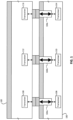
- FIG. 1 is a schematic representation of an illustrative stacked-die circuit structure with TSVs through which signals may be transmitted between the dies, in accordance with some implementations of the subject matter of this disclosure.
- Die 100 and die 102 form a stacked-die circuit structure.
- TSVs 104a-104c are formed in die 100 and communicatively connect die 100 and die 102.
- Transceivers 106, 110, and 114 transmit signals onto respective TSVs 104a, 104b, and104c from die 100 to die 102 while transceivers 108, 112, and 116 transmit signals onto respective TSVs 104a, 104b, and 104c from die 102 to die 100.
- any transceiver disposed on either die 100 or die 102 may transmit signals onto its respective TSV at any time. Accordingly, any signal transmitted onto a TSV may overlap, at least partially, with a signal transmitted in the opposing direction.
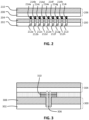
- FIG. 2 is a cross-sectional representation of an illustrative stacked-die circuit structure with TSVs, in accordance with some implementations of the subject matter of this disclosure.
- the stacked-die circuit structure of FIG. 2 is formed of die 200 containing a wiring layer 202 deposited on a device silicon layer 204 and die 206 containing a wiring layer 208 deposited on a device silicon layer 210.
- TSVs 212a-212i (of which TSVs 104a-104c of FIG. 1 are an illustrative subset) provide signaling pathways between die 200 and die 206.
- Hybrid bonds 214a-214i are a permanent bond that combines a dielectric bond with an embedded metal to form an interconnection between two stacked dies.
- hybrid bonding interconnection point may be fabricated on a first die by depositing a dielectric (e.g., a silicon oxide) over metallic (e.g., copper) pillars or other contact structures.
- die 200 is a memory device (e.g., SRAM) and die 206 is a system-on-a-chip (SOC) device.
- die 200 is a PHY and die 206 is a SERDES device.
- FIG. 3 is a cross-sectional representation of a TSV through which bidirectional signaling occurs between layers of a stacked-die circuit structure, in accordance with some implementations of the subject matter of this disclosure.
- Die 300 has a wiring layer 302 which may communicate with devices on other dies of the stacked-die circuit structure (e.g., die 304).
- TSV 306 begins in wiring layer 302 of die 300 and extends through device silicon layer 308 of die 300.
- a hybrid bond 310 communicatively couples TSV 306 with die 304, completing a signaling pathway between die 300 an die 304.
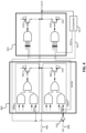
- FIG. 4 is a circuit diagram showing illustrative circuitry for calibrating signal levels of a signal driver to ensure accurate data transmission over a TSV, in accordance with some implementations of the subject matter of this disclosure.
- Signal driver elements 400a and 400b are used to transmit data onto a TSV.
- driver element 400a may be responsible for transmitting a logic one onto the TSV by pulling the output signal of the signal driver to a first signal level associated with a logic one (e.g., a more positive voltage level).
- Driver element 400b may similarly be responsible for transmitting a logic zero onto the TSV by pulling the output signal of the signal drive to a second signal level associated with a logic zero (e.g., a more negative voltage level).
- the driver elements may be embedded, at least in part, on one or both of the device layers of each die in the interconnect structure (e.g., dies 200 and 206).
- FET 402 pulls the signal in a positive direction and the output level or amount by which the other driver element switch, e.g., FET 404, pulls the signal in a negative direction, then signal present on the TSV may fall outside a threshold range when opposing signals transmit different values.
- driver elements 400 are periodically activated together and the resulting signal compared to a signal level range using comparator 412.
- the signal level should be halfway between the signal levels of each logic level. For example, if the signal level for a logic zero is 50mV and the signal level of a logic one is 700mV, the test signal generated by activating both signal drivers should be 375mV when the signal driver elements are properly matched.
- the transceiver may be configured to read any signal below 375mV as a logic zero and any signal above 375mV as a logic one. In some implementations, other ranges based on threshold deviations from the expected signal levels for each logic level may be used.
- FIG. 7 is a flow diagram representing an illustrative process for calibrating a signal driver, in accordance with some implementations of the subject matter of this disclosure.
- calibration circuitry initializes or retrieves a value T representing a time interval at which calibration is to occur. This time interval may be the duration of a clock cycle, meaning that calibration will occur at every clock cycle, or some multiple of the duration of the clock cycle.
- the calibration circuitry determines whether the interval has elapsed. If not ("No" at 704), the calibration circuitry waits.
- the calibration circuitry activates a signal driver of a signal transmitter to transmit a test signal on a bidirectional transmission medium of a TSV. Transmission of the test signal may be accomplished by activating a signal driver element responsible to transmitting a logic zero and simultaneously activating a second signal driver element responsible for transmitting a logic one. The resulting test signal should, therefore, have a signal level halfway between the signal level of a logic zero and the signal level of a logic one.
- the threshold may be up one quarter of the difference between the voltage level of a logic zero and the voltage level of a logic one. If a logic zero corresponds to 50mV and a logic one corresponds to 700mv, one quarter of the different between the two logic levels is 162.5mV. Accordingly, any voltage level at or below 212.5mV may be considered a logic zero and any voltage level at or above 537.5mV may be considered a logic one.
- the calibration circuitry may compare the voltage level of the test signal to one or more of these thresholds to determine if the voltage level of the signal is outside an expected range. In some implementations, the calibration circuitry may determine whether the voltage level of the test signal is above the threshold level of a logic zero (e.g., 212.5mV) and below the threshold level of a logic one (e.g., 537.5mV).
- the calibration circuitry determines that the level of the test signal is outside the expected range ("Yes" at 710), then, at 712, the calibration circuitry activates a boost circuit to bring the level of the test signal into the expected range. For example, if the test signal is within the threshold of a logic zero (e.g., below 212.5mV), a boost driver configured to raise the voltage level of the test signal is activated. Similarly, if the test signal is within the threshold of a logic one (e.g., above 537.5mV), a boost driver configured to lower the voltage level of the test signal is activated.
- the output power of an activated boost driver may be variable and controlled by the calibration circuitry in order to bring the test signal level into the expected range without overshooting.
Landscapes
- Physics & Mathematics (AREA)
- General Physics & Mathematics (AREA)
- Engineering & Computer Science (AREA)
- General Engineering & Computer Science (AREA)
- Logic Circuits (AREA)
- Tests Of Electronic Circuits (AREA)
- Dc Digital Transmission (AREA)
Applications Claiming Priority (1)
| Application Number | Priority Date | Filing Date | Title |
|---|---|---|---|
| US202363543023P | 2023-10-06 | 2023-10-06 |
Publications (2)
| Publication Number | Publication Date |
|---|---|
| EP4535357A2 true EP4535357A2 (de) | 2025-04-09 |
| EP4535357A3 EP4535357A3 (de) | 2025-06-18 |
Family
ID=93013857
Family Applications (1)
| Application Number | Title | Priority Date | Filing Date |
|---|---|---|---|
| EP24204776.9A Pending EP4535357A3 (de) | 2023-10-06 | 2024-10-04 | Gleichzeitige bidirektionale signalisierung in siliciumdurchkontaktierungen |
Country Status (2)
| Country | Link |
|---|---|
| EP (1) | EP4535357A3 (de) |
| KR (1) | KR20250050765A (de) |
Family Cites Families (6)
| Publication number | Priority date | Publication date | Assignee | Title |
|---|---|---|---|---|
| US7514954B2 (en) * | 2006-05-10 | 2009-04-07 | Micron Technology, Inc. | Method and apparatus for output driver calibration |
| JP2011081732A (ja) * | 2009-10-09 | 2011-04-21 | Elpida Memory Inc | 半導体装置及びその調整方法並びにデータ処理システム |
| US9105317B2 (en) * | 2012-01-13 | 2015-08-11 | Samsung Electronics Co., Ltd. | Memory system capable of calibrating output voltage level of semiconductor memory device and method of calibrating output voltage level of semiconductor memory device |
| US8766663B2 (en) * | 2012-06-18 | 2014-07-01 | International Business Machines Corporation | Implementing linearly weighted thermal coded I/O driver output stage calibration |
| US10998011B2 (en) * | 2018-08-21 | 2021-05-04 | Micron Technology, Inc. | Drive strength calibration for multi-level signaling |
| US11190188B2 (en) * | 2019-12-12 | 2021-11-30 | Electronics And Telecommunications Research Institute | Memory interface circuit including output impedance monitor and method of calibrating output impedance thereof |
-
2024
- 2024-10-04 EP EP24204776.9A patent/EP4535357A3/de active Pending
- 2024-10-07 KR KR1020240135674A patent/KR20250050765A/ko active Pending
Also Published As
| Publication number | Publication date |
|---|---|
| KR20250050765A (ko) | 2025-04-15 |
| EP4535357A3 (de) | 2025-06-18 |
Similar Documents
| Publication | Publication Date | Title |
|---|---|---|
| KR101124251B1 (ko) | 적층된 칩들에 아이디를 부여하는 시스템, 반도체 장치 및 그 방법 | |
| US20070289772A1 (en) | Electronic Circuit | |
| US7546106B2 (en) | Electronic circuit | |
| US8477855B2 (en) | Signal transmission system and semiconductor integrated circuit device | |
| US8526251B2 (en) | Semiconductor apparatus, method for delaying signal thereof, stacked semiconductor memory apparatus, and method for generating signal thereof | |
| TW594787B (en) | Methods and apparatus for adaptively adjusting a data receiver | |
| US7808277B2 (en) | Bidirectional signal separation module for a bus converter | |
| CN104425411A (zh) | 半导体器件和半导体器件的操作方法 | |
| KR20140146822A (ko) | 반도체 장치의 테스트 회로 및 방법 | |
| US20110227604A1 (en) | Receiving circuit and methods for controlling and testing the same | |
| WO2014172301A1 (en) | Flexible input/output transceiver | |
| Poulton et al. | A 0.54 pJ/b 20Gb/s ground-referenced single-ended short-haul serial link in 28nm CMOS for advanced packaging applications | |
| EP4535357A2 (de) | Gleichzeitige bidirektionale signalisierung in siliciumdurchkontaktierungen | |
| US20210183412A1 (en) | Multi-chip devices | |
| US20250119219A1 (en) | Simultaneous bidirectional signaling in through-silicon vias | |
| US9536807B2 (en) | Stack package and semiconductor integrated circuit device including a variable voltage | |
| KR102810483B1 (ko) | 테스트회로를 포함하는 반도체장치 | |
| CN214477449U (zh) | 一种多芯片封装结构及其微系统 | |
| US11810638B2 (en) | Memory device including multiple memory chips and data signal lines and a method of operating the memory device | |
| CN102568562A (zh) | 叠层封装和用于选择叠层封装中的芯片的方法 | |
| US20090322383A1 (en) | Semiconductor device, signal transmitter, and signal transmission method | |
| US20090067616A1 (en) | CAN echo cancellation level shifter | |
| Furuta et al. | 6 Tbps/W, 1 Tbps/mm 2, 3D interconnect using adaptive timing control and low capacitance TSV | |
| US9202802B2 (en) | Semiconductor apparatus having through via capable of testing connectivity of through via | |
| KR102047932B1 (ko) | 임피던스 조정 기능을 갖는 적층형 반도체 회로 |
Legal Events
| Date | Code | Title | Description |
|---|---|---|---|
| PUAI | Public reference made under article 153(3) epc to a published international application that has entered the european phase |
Free format text: ORIGINAL CODE: 0009012 |
|
| STAA | Information on the status of an ep patent application or granted ep patent |
Free format text: STATUS: THE APPLICATION HAS BEEN PUBLISHED |
|
| AK | Designated contracting states |
Kind code of ref document: A2 Designated state(s): AL AT BE BG CH CY CZ DE DK EE ES FI FR GB GR HR HU IE IS IT LI LT LU LV MC ME MK MT NL NO PL PT RO RS SE SI SK SM TR |
|
| PUAL | Search report despatched |
Free format text: ORIGINAL CODE: 0009013 |
|
| AK | Designated contracting states |
Kind code of ref document: A3 Designated state(s): AL AT BE BG CH CY CZ DE DK EE ES FI FR GB GR HR HU IE IS IT LI LT LU LV MC ME MK MT NL NO PL PT RO RS SE SI SK SM TR |
|
| RIC1 | Information provided on ipc code assigned before grant |
Ipc: G11C 29/50 20060101ALI20250512BHEP Ipc: G11C 29/02 20060101ALI20250512BHEP Ipc: G11C 7/22 20060101AFI20250512BHEP |
|
| STAA | Information on the status of an ep patent application or granted ep patent |
Free format text: STATUS: REQUEST FOR EXAMINATION WAS MADE |
|
| 17P | Request for examination filed |
Effective date: 20250730 |