EP4530709A1 - Verfahren zur herstellung planarisierter oberflächen in schichtstrukturen zur herstellung optoelektronischer bauelemente - Google Patents
Verfahren zur herstellung planarisierter oberflächen in schichtstrukturen zur herstellung optoelektronischer bauelemente Download PDFInfo
- Publication number
- EP4530709A1 EP4530709A1 EP23200213.9A EP23200213A EP4530709A1 EP 4530709 A1 EP4530709 A1 EP 4530709A1 EP 23200213 A EP23200213 A EP 23200213A EP 4530709 A1 EP4530709 A1 EP 4530709A1
- Authority
- EP
- European Patent Office
- Prior art keywords
- layer
- layered structure
- preferred
- thickness
- section
- Prior art date
- Legal status (The legal status is an assumption and is not a legal conclusion. Google has not performed a legal analysis and makes no representation as to the accuracy of the status listed.)
- Withdrawn
Links
Images

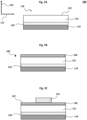


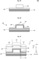
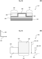


Classifications
-
- G—PHYSICS
- G02—OPTICS
- G02B—OPTICAL ELEMENTS, SYSTEMS OR APPARATUS
- G02B6/00—Light guides; Structural details of arrangements comprising light guides and other optical elements, e.g. couplings
- G02B6/10—Light guides; Structural details of arrangements comprising light guides and other optical elements, e.g. couplings of the optical waveguide type
- G02B6/12—Light guides; Structural details of arrangements comprising light guides and other optical elements, e.g. couplings of the optical waveguide type of the integrated circuit kind
- G02B6/13—Integrated optical circuits characterised by the manufacturing method
-
- H—ELECTRICITY
- H10—SEMICONDUCTOR DEVICES; ELECTRIC SOLID-STATE DEVICES NOT OTHERWISE PROVIDED FOR
- H10F—INORGANIC SEMICONDUCTOR DEVICES SENSITIVE TO INFRARED RADIATION, LIGHT, ELECTROMAGNETIC RADIATION OF SHORTER WAVELENGTH OR CORPUSCULAR RADIATION
- H10F30/00—Individual radiation-sensitive semiconductor devices in which radiation controls the flow of current through the devices, e.g. photodetectors
- H10F30/10—Individual radiation-sensitive semiconductor devices in which radiation controls the flow of current through the devices, e.g. photodetectors the devices being sensitive to infrared radiation, visible or ultraviolet radiation, and having no potential barriers, e.g. photoresistors
-
- H—ELECTRICITY
- H10—SEMICONDUCTOR DEVICES; ELECTRIC SOLID-STATE DEVICES NOT OTHERWISE PROVIDED FOR
- H10F—INORGANIC SEMICONDUCTOR DEVICES SENSITIVE TO INFRARED RADIATION, LIGHT, ELECTROMAGNETIC RADIATION OF SHORTER WAVELENGTH OR CORPUSCULAR RADIATION
- H10F71/00—Manufacture or treatment of devices covered by this subclass
- H10F71/121—The active layers comprising only Group IV materials
-
- G—PHYSICS
- G02—OPTICS
- G02F—OPTICAL DEVICES OR ARRANGEMENTS FOR THE CONTROL OF LIGHT BY MODIFICATION OF THE OPTICAL PROPERTIES OF THE MEDIA OF THE ELEMENTS INVOLVED THEREIN; NON-LINEAR OPTICS; FREQUENCY-CHANGING OF LIGHT; OPTICAL LOGIC ELEMENTS; OPTICAL ANALOGUE/DIGITAL CONVERTERS
- G02F2201/00—Constructional arrangements not provided for in groups G02F1/00 - G02F7/00
- G02F2201/06—Constructional arrangements not provided for in groups G02F1/00 - G02F7/00 integrated waveguide
-
- H—ELECTRICITY
- H10—SEMICONDUCTOR DEVICES; ELECTRIC SOLID-STATE DEVICES NOT OTHERWISE PROVIDED FOR
- H10F—INORGANIC SEMICONDUCTOR DEVICES SENSITIVE TO INFRARED RADIATION, LIGHT, ELECTROMAGNETIC RADIATION OF SHORTER WAVELENGTH OR CORPUSCULAR RADIATION
- H10F77/00—Constructional details of devices covered by this subclass
- H10F77/10—Semiconductor bodies
- H10F77/12—Active materials
- H10F77/122—Active materials comprising only Group IV materials
-
- H—ELECTRICITY
- H10—SEMICONDUCTOR DEVICES; ELECTRIC SOLID-STATE DEVICES NOT OTHERWISE PROVIDED FOR
- H10F—INORGANIC SEMICONDUCTOR DEVICES SENSITIVE TO INFRARED RADIATION, LIGHT, ELECTROMAGNETIC RADIATION OF SHORTER WAVELENGTH OR CORPUSCULAR RADIATION
- H10F77/00—Constructional details of devices covered by this subclass
- H10F77/10—Semiconductor bodies
- H10F77/16—Material structures, e.g. crystalline structures, film structures or crystal plane orientations
Definitions
- the invention pertains to methods for producing a layered structure, wherein said layered structure preferably comprises a waveguide.
- the invention also pertains to a method for producing an opto-electronic device using the layered structure, wherein said opto-electronic device preferably comprises one or more graphene layers.
- Opto-electronic devices such as modulators and photodetectors are important electronic components for optical communication systems, e.g., data transmission via fibre optics. Some of the important parameters for these devices are bandwidth, operation speed, extinction ratio, insertion loss, energy consumption, and footprint.
- silicon-based modulators have a number of disadvantages. For example, silicon-based modulators have a narrow bandwidth.
- silicon-based modulators have to be produced as part of a front-end-of-line process.
- silicon-based modulators cannot easily be integrated with newer technologies that are being developed in the electronic industry.
- graphene-based modulators have a number of advantages.
- graphene-based modulators have a broader bandwidth compared to silicon-based modulators.
- graphene-based modulators can be integrated with other electronic components as part of a back-end-of-line process, without requiring significant development to enable the integration.
- Graphene-based modulators can also be more easily integrated with newer technologies in the electronic industry.
- Graphene-based modulators further allow for a better use of surface area, and thus a more compact electronic device or system. Examples of graphene-based modulators are disclosed in, e.g., Liu et al. (2011), A graphene-based broadband optical modulator, Nature, 474, 65 , and Liu et al. (2012), Double-layer graphene optical modulator, Nano Letter, 12, 1482 .
- any surface onto which the graphene is deposited is highly planarized.
- Discontinuities in said surface can lead to stresses in the graphene layer, which in turn can lead to the graphene layer breaking. This is especially the case if the graphene layer is not conformal with the discontinuities.
- a graphene layer that is conformal with the discontinuities also leads to problems with controlling electrical properties, such as potential difference and electric fields, in the opto-electronic device.
- to obtain a sufficiently planarized surface that also reduces the distances between the waveguide and the one or more graphene layers is still an open problem to be solved.
- An object of the present invention is to at least partially overcome at least one of the disadvantages encountered in the state of the art.
- An example of an electrically conducting element is a graphene layer or a perovskite layer.
- An example of an element of the first kind is a waveguide adapted and arranged for the propagation of electromagnetic waves.
- An example of an electrically conducting element is a graphene layer or a perovskite layer.
- a 1 st embodiment of the invention is a first method for producing a layered structure, comprising the steps of
- the layered structure is obtained after the reduction step has been completed. In another aspect of the 1 st embodiment, it is preferred that the layered structure is obtained following the completion of the reduction step and at least one further method step. In an aspect of the 1 st embodiment, it is preferred that a cross-sectional cut of the intermediate layered structure, made at the position of the element of the first kind, has the following layers and element, in this order: the element of the first kind, the layer of the second kind, and the first section of the first layer of the further kind.
- feature b. the following combinations are preferred aspects of the embodiment: b.i; b.ii; b.i + b.ii.
- the combination b.i + b.ii is particularly preferred.
- the first thickness-reducing technique is chemical-mechanical polishing.
- the first thickness d 3A is reduced such that the layer of the second kind is at least partially exposed.
- the element of the first kind is a waveguide that is adapted and arranged for the propagation of electromagnetic waves.
- the layered structure that is obtainable from the 1 st embodiment is suitable to be used for the production of an opto-electronic device, more preferably an opto-electronic device comprising graphene.
- the at least one property varies between the layer of the second kind and the first layer of the further kind.
- the at least one property is at least one or all of the following:
- This preferred embodiment is a 2 nd embodiment of the invention, that preferably depends on the 1 st embodiment of the invention.
- all combinations of the features a. to k. are preferred aspects of the embodiment.
- the combination of the features a. to f. are more preferred aspects of the embodiment. These combinations are e.g., a; b; c; d; e; f; a+b; a+c; a+d; a+e; a+f; b+c; b+d; b+e; b+f; c+d; c+e; c+f; d+e; d+f; e+f; a+b+c; a+b+d; a+b+e; a+b+f; a+c+d; a+c+e; a+c+f; a+d+e; a+d+f; a+e+f; b+c+d; b+c+f; b+c+f; b+c+f; b+c+f; b+c+f
- all possible combination of the features b. to d. are particularly preferred aspects of the embodiment. These combinations are, e.g., b; c; d; b+c; b+d; c+d; b+c+d.
- This preferred embodiment is a 3 rd embodiment of the invention, that preferably depends on any of the 1 st to 2 nd embodiments of the invention.
- all possible combination of the features a. to d. are preferred aspects of the embodiment. These combinations are e.g., a; b; c; d; a+b; a+c; a+d; b+c; b+d; c+d; a+b+c; a+b+d; a+c+d; b+c+d; a+b+c+d.
- all possible combination of the features b. and c. are particularly preferred aspects of the embodiment. These combinations are e.g., b; c; b+c.
- feature c. is particularly preferred.
- This preferred embodiment is a 4 th embodiment of the invention, that preferably depends on any of the 1 st to 3 rd embodiments of the invention.
- all possible combination of the features a. to d. are preferred aspects of the embodiment. These combinations are e.g., a; b; c; d; a+b; a+c; a+d; b+c; b+d; c+d; a+b+c; a+b+d; a+c+d; b+c+d; a+b+c+d.
- all possible combination of the features b. and c. are particularly preferred aspects of the embodiment. These combinations are e.g., b; c; b+c.
- feature c. is particularly preferred.
- This preferred embodiment is a 5 th embodiment of the invention, that preferably depends on any of the 3 rd to 4 th embodiments of the invention.
- all possible combination of the features a. to d. are preferred aspects of the embodiment. These combinations are e.g., a; b; c; d; a+b; a+c; a+d; b+c; b+d; c+d; a+b+c; a+b+d; a+c+d; b+c+d; a+b+c+d.
- all possible combination of the features a. and b. are more preferred aspects of the embodiment. These combinations are e.g., a; b; a+b.
- feature b. is particularly preferred.
- the first etch rate of the first layer of the further kind is in the range of 4 to 200 times, more preferably in the range of 5 to 150 times, and further preferably in the range of 10 to 100 times larger than the first etch rate of the layer of the second kind.
- the first material removal rate of the first layer of the further kind is in the range of 1.5 to 200 times, more preferably in the range of 5 to 150 times, and further preferably in the range of 10 to 100 times larger than the first material removal rate of the layer of the second kind.
- the first etch rate of the element of the first kind is in the range of 4 to 200 times, more preferably in the range of 5 to 150 times, and further preferably in the range of 10 to 100 times larger than the first etch rate of the layer of the second kind.
- the first material removal rate of the element of the first kind is in the range of 1.5 to 200 times, more preferably in the range of 5 to 150 times, and further preferably in the range of 10 to 100 times larger than the first material removal rate of the layer of the second kind.
- the first section has a first thickness d 3A ⁇ 50 nm, more preferably d 3A ⁇ 20 nm, even more preferably d 3A ⁇ 10 nm, further preferably d 3A ⁇ 5 nm, further preferably d 3A ⁇ 2 nm, and even further preferably d 3A ⁇ 1 nm.
- This preferred embodiment is a 6 th embodiment of the invention, that preferably depends on any of the 1 st to 5 th embodiments of the invention.
- This preferred embodiment is a 7 th embodiment of the invention, that preferably depends on any of the 1 st to 6 th embodiments of the invention.
- all possible combination of the features a. and b. are preferred aspects of the embodiment. These combinations are e.g., a; b; a+b.
- it is preferred that the thickness d 2 is measured prior to the start of the reduction step in the 1 st embodiment (step b.).
- the thickness d 2 of the layer of the second kind is in the range of 0.1 nm to 80 nm, more preferably in the range of 0.2 nm to 60 nm, even more preferably in the range of 0.5 nm to 40 nm, even more preferably in the range from 1 nm to 30 nm, further preferably in the range of 2 nm to 25 nm, further preferably in the range of 5 nm to 20 nm, and even further preferably in the range of 5 nm to 10 nm.
- the first distance l 3 is in the range of 0.1 nm to 80 nm, more preferably in the range of 0.2 nm to 60 nm, even more preferably in the range of 0.5 nm to 40 nm, even more preferably in the range from 1 nm to 30 nm, further preferably in the range of 2 nm to 25 nm, further preferably in the range of 5 nm to 20 nm, and even further preferably in the range of 5 nm to 10 nm.
- This preferred embodiment is an 8 th embodiment of the invention, that preferably depends on any of the 1 st to 7 th embodiments of the invention.
- all possible combination of the features a. to c. are preferred aspects of the embodiment. These combinations are e.g., a; b; c; a+b; a+c; b+c; a+b+c.
- it is preferred that at least one, preferably all thickness are prior to the start of the reduction step in the 1 st embodiment (step b.). In this aspect, these thicknesses include d 1 , d 3A , and d 3B .
- both the first thickness d 3A and the further thickness d 3B of the first layer of the further kind are reduced using the first thickness-reducing technique, wherein the first thickness d 3A is reduced by a value V 3A , the further thickness d 3B is reduced by a value V 3B , and wherein V 3A and V 3B vary by less than 20 %, preferably by less than 10 %, and more preferably by less than 5 %.
- This preferred embodiment is a 9 th embodiment of the invention, that preferably depends on any of the 1 st to 8 th embodiments of the invention.
- the first thickness-reducing technique is at least one of the following:
- This preferred embodiment is a 10 th embodiment of the invention, that preferably depends on any of the 1 st to 9 th embodiments of the invention.
- all possible combination of the features a. to d. are preferred aspects of the embodiment. These combinations are e.g., a; b; c; d; a+b; a+c; a+d; b+c; b+d; c+d; a+b+c; a+b+d; a+c+d; b+c+d; a+b+c+d.
- chemical-mechanical polishing is particularly preferred.
- the method further comprises the steps of:
- This preferred embodiment is an 11 th embodiment of the invention, that preferably depends on any of the 1 st to 10 th embodiments of the invention.
- the intermediate layered structure is obtained following the completion of the steps of the embodiment.
- the method further comprises the steps of:
- This preferred embodiment is a 12 th embodiment of the invention, that preferably depends on any of the 1 st to 10 th embodiments of the invention.
- the intermediate layered structure is obtained following the completion of the steps of the embodiment.
- the thickness of at least one section of the layer of the first kind, the thickness of at least one section of the layer of the second kind, or both are reduced using at least one or all of the following:
- This preferred embodiment is a 13 th embodiment of the invention, that preferably depends on any of the 11 th to 12 th embodiments of the invention.
- the method further comprises the following steps, performed after the step of reducing the first thickness d 3A and preferably the further thickness d 3B of the first layer of the further kind (step b. in the 1 st embodiment):
- This preferred embodiment is a 14 th embodiment of the invention, that preferably depends on any of the 1 st to 13 th embodiments of the invention.
- the thickness d 4 of the further layer of the further kind, prior to being reducing in step C. is at least 1.1 times, more preferably at least 1.5 times, even more preferably at least 2 times, and further preferably at least 4 times larger than the depth D R of the recess.
- the first surface of the further section of the first layer of the further kind is arranged at a height h 3B
- a first surface of the further layer of the further kind is arranged at a height h 4
- This preferred embodiment is a 15 th embodiment of the invention, that preferably depends on the 14 th embodiments of the invention.
- the height difference given in aspect b. applies after the reduction step C.] in the 14 th preferred embodiment has been completed.
- This preferred embodiment is a 16 th embodiment of the invention, that preferably depends on any of the 14 th to 15 th embodiments of the invention.
- all possible combination of the features a. to c. are preferred aspects of the embodiment. These combinations are e.g., a; b; c; a+b; a+c; b+c; a+b+c. In an aspect of the 16 th embodiment, feature a. is particularly preferred.
- This preferred embodiment is a 17 th embodiment of the invention, that preferably depends on any of the 14 th to 16 th embodiments of the invention.
- This preferred embodiment is an 18 th embodiment of the invention, that preferably depends on any of the 16 th to 17 th embodiments of the invention.
- all possible combination of the features a. to d. are preferred aspects of the embodiment. These combinations are e.g., a; b; c; d; a+b; a+c; a+d; b+c; b+d; c+d; a+b+c; a+b+d; a+c+d; b+c+d; a+b+c+d.
- all possible combination of the features a. and c. are more preferred aspects of the embodiment. These combinations are e.g., a; c; a+c.
- feature a. is particularly preferred.
- the further etch rate of the layer of the second kind is in the range of 4 to 200 times, more preferably in the range of 5 to 150 times, and further preferably in the range of 10 to 100 times larger than the further etch rate of the first layer of the further kind.
- the further material removal rate of the layer of the second kind is in the range of 1.5 to 200 times, more preferably in the range of 5 to 150 times, and further preferably in the range of 10 to 100 times larger than the further material removal rate of the first layer of the further kind.
- the further etch rate of the layer of the second kind is in the range of 4 to 200 times, more preferably in the range of 5 to 150 times, and further preferably in the range of 10 to 100 times larger than the further etch rate of the element of the first kind.
- the further material removal rate of the layer of the second kind is in the range of 1.5 to 200 times, more preferably in the range of 5 to 150 times, and further preferably in the range of 10 to 100 times larger than the further material removal rate of the element of the first kind.
- the further thickness-reducing technique is at least one or all of the following:
- This preferred embodiment is a 19 th embodiment of the invention, that preferably depends on any of the 14 th to 18 th embodiments of the invention.
- all possible combination of the features a. to d. are preferred aspects of the embodiment. These combinations are e.g., a; b; c; d; a+b; a+c; a+d; b+c; b+d; c+d; a+b+c; a+b+d; a+c+d; b+c+d; a+b+c+d.
- all possible combination of the features a. to c. are particularly preferred aspects of the embodiment. These combinations are e.g., a; b; c; a+b; a+c; b+c; a+b+c.
- wet etching is particularly preferred.
- the thickness d 4 of the further layer of the further kind is reduced using at least one of the following:
- This preferred embodiment is a 20 th embodiment of the invention, that preferably depends on any of the 14 th to 19 th embodiments of the invention.
- all possible combination of the features a. to d. are preferred aspects of the embodiment. These combinations are e.g., a; b; c; d; a+b; a+c; a+d; b+c; b+d; c+d; a+b+c; a+b+d; a+c+d; b+c+d; a+b+c+d.
- the duration of the chemical-mechanical polishing of the first thickness-reducing technique is longer than the duration of the chemical-mechanical polishing of the 20 th embodiment.
- chemical-mechanical polishing is particularly preferred.
- This preferred embodiment is a 21 st embodiment of the invention, that preferably depends on any of the 1 st to 20 th embodiments of the invention.
- all possible combination of the features a. to c. are preferred aspects of the embodiment. These combinations are e.g., a; b; c; a+b; a+c; b+c; a+b+c. In an aspect of the 21 st embodiment, feature a. is particularly preferred.
- At least one layer is deposited using at least one or all of the following:
- This preferred embodiment is a 22 nd embodiment of the invention, that preferably depends on any of the 1 st to 21 st embodiments of the invention.
- This preferred embodiment is a 23 rd embodiment of the invention, that preferably depends on any of the 1 st to 22 nd embodiments of the invention.
- all possible combination of the features a. to c. are preferred aspects of the embodiment. These combinations are e.g., a; b; c; a+b; a+c; b+c; a+b+c. In an aspect of the 23 rd embodiment, the combination of the features b. and c. are particularly preferred.
- the element of the first kind comprises at least 50 wt-%, more preferably at least 65 wt-%, even more preferably at least 75 wt-%, further preferably at least 85 wt-%, and even further preferably at least 95 wt-%, based on a total weight of the element of the first kind, of a nitride, more preferably silicon nitride.
- This preferred embodiment is a 24 th embodiment of the invention, that preferably depends on any of the 1 st to 23 rd embodiments of the invention.
- all possible combination of the features a. to d. are preferred aspects of the embodiment. These combinations are e.g., a; b; c; d; a+b; a+c; a+d; b+c; b+d; c+d; a+b+c; a+b+d; a+c+d; b+c+d; a+b+c+d.
- all possible combination of the features a. and b. are particularly preferred aspects of the embodiment. These combinations are e.g., a; b; a+b.
- the refractive index of the layer of the second kind is in the range of 1.05 to 4 times larger, more preferably in the range of 1.3 to 3.7 times larger, and further preferably in the range of 1.6 to 2.7 times larger than the refractive index of the element of the first kind.
- the layer of the second kind comprises less than 20 wt-%, more preferably less than 15 wt-%, even more preferably less than 10 wt-%, further preferably less than 5 wt-%, and even further preferably less than 1.5 wt-%, based on a total weight of the layer of the second kind, of a nitride, more preferably silicon nitride.
- the first method for producing a layered structure at least one or all of the following applies to the first layer of the further kind, the further layer of the further kind, or both:
- This preferred embodiment is a 25 th embodiment of the invention, that preferably depends on any of the 1 st to 24 th embodiments of the invention.
- all possible combination of the features a. to c. are preferred aspects of the embodiment. These combinations are e.g., a; b; c; a+b; a+c; b+c; a+b+c.
- the intermediate layered structure is superimposed on a wafer layer.
- This preferred embodiment is a 26 th embodiment of the invention, that preferably depends on any of the 1 st to 25 th embodiments of the invention.
- a 27 th embodiment of the invention is a second method for producing a layered structure, comprising the steps of
- the layered structure is obtained after the oxidising step has been completed. In another aspect of the 27 th embodiment, it is preferred that the layered structure is obtained following the completion of the oxidising step and at least one further method step. In an aspect of the 27 th embodiment, it is preferred that the oxidising step b. is performed in an environment that has at a pressure of at least 1 atmosphere, more preferably at least 2 atmospheres, and further preferably at least 3 atmospheres. In an aspect of the 27 th embodiment, it is preferred that the oxidising step b.
- the oxidising step b. is performed in an environment that has a temperature in the range of 200 °C to 1000 °C, more preferably in the range of 300 °C to 900 °C, and further preferably in the range of 350 °C to 850 °C.
- the temperature of the environment is 500 °C or less, more preferably 450 °C or less, and further preferably 400 °C or less.
- the element of the first kind is a waveguide that is adapted and arranged for the propagation of electromagnetic waves.
- the layered structure that is obtainable from the 27 th embodiment is suitable to be used for the production of an opto-electronic device, more preferably an opto-electronic device comprising graphene.
- the oxidising step is performed using at least one or all of the following:
- This preferred embodiment is a 28 th embodiment of the invention, that preferably depends on the 27 th embodiment of the invention.
- all possible combination of the features a. to c. are preferred aspects of the embodiment. These combinations are e.g., a; b; c; a+b; a+c; b+c; a+b+c.
- feature a. it is preferred that the oxygen is in the form of at least one oxygen radical. Examples of an oxygen radical include a peroxide, a superoxide, a hydroxyl radical, singlet oxygen, and alpha-oxygen.
- feature b. it is preferred that the water is in the form of a gas, e.g., water vapour.
- an oxidation rate of the element of the first kind is larger than an oxidation rate of the further section of the first layer of the further kind.
- This preferred embodiment is a 29 th embodiment of the invention, that preferably depends on any of the 27 th to 28 th embodiments of the invention.
- the oxidation rate of the element of the first kind is at least 1.1 times, preferably at least 5 times, more preferably at least 10 times, more preferably at least 20 times, more preferably at least 50 times, more preferably at least 100 times, more preferably at least 200 times, more preferably at least 500 times, further preferably at least 1000 times, further preferably at least 2000 times, and even further preferably at least 5000 times larger than the oxidation rate of the further section of the first layer of the further kind.
- This preferred embodiment is a 30 th embodiment of the invention, that preferably depends on any of the 27 th to 29 th embodiments of the invention.
- all possible combination of the features a. and b. are preferred aspects of the embodiment. These combinations are e.g., a; b; a+b.
- This preferred embodiment is a 31 st embodiment of the invention, that preferably depends on any of the 27 th to 30 th embodiments of the invention.
- all possible combination of the features a. to c. are preferred aspects of the embodiment. These combinations are e.g., a; b; c; a+b; a+c; b+c; a+b+c.
- oxide in the 3 1 st embodiment include silicon dioxide, aluminium oxide, zirconium dioxide, hafnium oxide, titanium dioxide, niobium pentoxide, tantalum pentoxide, lanthanum oxide.
- At least 80 wt-%, preferably at least 90 wt-%, and further preferably at least 99 wt-% of the further section of the first layer of the further kind has the same chemical composition as the layer of the even-further kind.
- This preferred embodiment is a 32 nd embodiment of the invention, that preferably depends on any of the 27 th to 3 1 st embodiments of the invention.
- This preferred embodiment is a 33 rd embodiment of the invention, that preferably depends on any of the 27 th to 32 nd embodiments of the invention.
- the etch rate is either a first etch rate or a further etch rate.
- the material removal rate is either a first material removal rate or a further material removal rate.
- the chemical reaction rate is either a first chemical reaction rate or a further chemical reaction rate.
- This preferred embodiment is a 34 th embodiment of the invention, that preferably depends on any of the 27 th to 32 nd embodiments of the invention.
- the etch rate is either a first etch rate or a further etch rate.
- the material removal rate is either a first material removal rate or a further material removal rate.
- the chemical reaction rate is either a first chemical reaction rate or a further chemical reaction rate.
- the etch rates of the layer of the even-further kind and the layer of the further kind differ by at least 2 times, preferably at least 3 times, more preferably at least 4 times, more preferably at least 5 times, more preferably at least 10 times, more preferably at least 20 times, more preferably at least 50 times, more preferably at least 100 times, further preferably at least 200 times, further preferably at least 500 times, and even further preferably at least 1000 times.
- This preferred embodiment is a 35 th embodiment of the invention, that preferably depends on any of the 33 rd to 34 th embodiments of the invention.
- the etch rates differ by 4 to 200 times, more preferably by 5 to 150 times, and further preferably by 10 to 100 times.
- the first distance l 3 is l 3 ⁇ 80 nm, preferably l 3 ⁇ 60 nm, more preferably l 3 ⁇ 40 nm, even more preferably l 3 ⁇ 20 nm, further preferably l 3 ⁇ 10 nm, further preferably l 3 ⁇ 5 nm, further preferably l 3 ⁇ 2 nm, and even further preferably l 3 ⁇ 1 nm.
- This preferred embodiment is a 36 th embodiment of the invention, that preferably depends on any of the 27 th to 35 th embodiments of the invention.
- the first distance l 3 is in the range of 0.1 nm to 80 nm, more preferably in the range of 0.2 nm to 60 nm, even more preferably in the range of 0.5 nm to 40 nm, even more preferably in the range from 1 nm to 30 nm, further preferably in the range of 2 nm to 25 nm, further preferably in the range of 5 nm to 20 nm, and even further preferably in the range of 5 nm to 10 nm.
- This preferred embodiment is a 37 th embodiment of the invention, that preferably depends on any of the 27 th to 36 th embodiments of the invention.
- all possible combination of the features a. and b. are preferred aspects of the embodiment. These combinations are e.g., a; b; a+b.
- it is preferred that at least one, preferably all thickness are measured prior to the start of the oxidising step in the 27 th embodiment (step b.). These thicknesses include d 1 , and d 3B .
- the method further comprises the step of reducing a thickness d 5 of the layer of the even-further kind.
- This preferred embodiment is a 38 th embodiment of the invention, that preferably depends on any of the 27 th to 37 th embodiments of the invention.
- the thickness d 5 is reduced after the oxidising step in the 27 th embodiment (step b.).
- the thickness d 5 is reduced using least one of the following:
- This preferred embodiment is a 39 th embodiment of the invention, that preferably depends on the 38 th embodiment of the invention.
- all possible combination of the features a. to d. are preferred aspects of the embodiment. These combinations are e.g., a; b; c; d; a+b; a+c; a+d; b+c; b+d; c+d; a+b+c; a+b+d; a+c+d; b+c+d; a+b+c+d.
- the method further comprises the steps of:
- This preferred embodiment is a 40 th embodiment of the invention, that preferably depends on any of the 27 th to 39 th embodiments of the invention.
- the intermediate layered structure is obtained following the completion of the steps of the embodiment.
- At least one layer is deposited using at least one or all of the following:
- This preferred embodiment is a 41 st embodiment of the invention, that preferably depends on the 40 th embodiment of the invention.
- This preferred embodiment is a 42 nd embodiment of the invention, that preferably depends on any of the 27 th to 41 st embodiments of the invention.
- all possible combination of the features a. to c. are preferred aspects of the embodiment. These combinations are e.g., a; b; c; a+b; a+c; b+c; a+b+c. In an aspect of the 42 nd embodiment, the combination of the features b. and c are particularly preferred.
- the element of the first kind comprises at least 50 wt-%, more preferably at least 65 wt-%, even more preferably at least 75 wt-%, further preferably at least 85 wt-%, and even further preferably at least 95 wt-%, based on a total weight of the element of the first kind, of a nitride, more preferably silicon nitride.
- the second method for producing a layered structure at least one or all of the following applies to the first layer of the further kind, the layer of the even-further kind, or both:
- This preferred embodiment is a 43 rd embodiment of the invention, that preferably depends on any of the 27 th to 42 nd embodiments of the invention.
- all possible combination of the features a. to c. are preferred aspects of the embodiment. These combinations are e.g., a; b; c; a+b; a+c; b+c; a+b+c.
- the intermediate layered structure is superimposed on a wafer layer.
- This preferred embodiment is a 44 th embodiment of the invention, that preferably depends on any of the 27 th to 43 rd embodiments of the invention.
- a 45 th embodiment of the invention is a layered structure obtainable by any of the methods, according to the invention, for producing a layered structure, preferably a layered structure obtainable by any of the methods according to any of the 1 st to 44 th embodiments of the invention.
- the layered structure is obtainable by the first method for producing a layered structure, more preferably the first method according to any of the 1 st to 26 th embodiments of the invention.
- the layered structure is obtainable by the second method for producing a layered structure, more preferably the second method according to any of the 27 th to 44 th embodiments of the invention.
- a 46 th embodiment of the invention is a first layered structure comprising
- the element of the first kind is a waveguide adapted and arranged for the propagation of electromagnetic waves.
- This preferred embodiment is a 47 th embodiment of the invention, that preferably depends on the 46 th embodiment of the invention.
- all possible combination of the features a. to c. are preferred aspects of the embodiment. These combinations are e.g., a; b; c; a+b; a+c; b+c; a+b+c.
- a 48 th embodiment of the invention is a second layered structure comprising
- the element of the first kind is a waveguide adapted and arranged for the propagation of electromagnetic waves.
- This preferred embodiment is a 49 th embodiment of the invention, that preferably depends on the 48 th embodiment of the invention.
- all possible combination of the features a. to c. are preferred aspects of the embodiment. These combinations are e.g., a; b; c; a+b; a+c; b+c; a+b+c.
- At least one or all of the following differs between the levelling layer and the element of the first kind:
- This preferred embodiment is a 50 th embodiment of the invention, that preferably depends on any of the 48 th to 49 th embodiments of the invention.
- all combinations of the features a. to k. are preferred aspects of the embodiment.
- the combination of the features a. to f. are more preferred aspects of the embodiment. These combinations are e.g., a; b; c; d; e; f; a+b; a+c; a+d; a+e; a+f; b+c; b+d; b+e; b+f; c+d; c+e; c+f; d+e; d+f; e+f; a+b+c; a+b+d; a+b+e; a+b+f; a+c+d; a+c+e; a+c+f; a+d+e; a+d+f; a+e+f; b+c+d; b+c+f; b+c+f; b+c+f;
- all possible combination of the features b. to d. are particularly preferred aspects of the embodiment. These combinations are, e.g., b; c; d; b+c; b+d; c+d; b+c+d.
- At least one or all of the following differs between the levelling layer and the further section of the first layer of the further kind:
- This preferred embodiment is a 51 st embodiment of the invention, that preferably depends on any of the 48 th to 50 th embodiments of the invention.
- all combinations of the features a. to k. are preferred aspects of the embodiment.
- the combination of the features a. to f. are more preferred aspects of the embodiment. These combinations are e.g., a; b; c; d; e; f; a+b; a+c; a+d; a+e; a+f; b+c; b+d; b+e; b+f; c+d; c+e; c+f; d+e; d+f; e+f; a+b+c; a+b+d; a+b+e; a+b+f; a+c+d; a+c+e; a+c+f; a+d+e; a+d+f; a+e+f; b+c+d; b+c+f; b+c+f; b+c+f; b+c+f; b+c+f
- all possible combination of the features b. to d. are particularly preferred aspects of the embodiment. These combinations are, e.g., b; c; d; b+c; b+d; c+d; b+c+d.
- the levelling layer is one of the following:
- This preferred embodiment is a 52 nd embodiment of the invention, that preferably depends on any of the 48 th to 51 st embodiments of the invention.
- This preferred embodiment is a 53 rd embodiment of the invention, that preferably depends on any of the 48 th to 52 nd embodiments of the invention.
- all possible combination of the features a. to c. are preferred aspects of the embodiment. These combinations are e.g., a; b; c; a+b; a+c; b+c; a+b+c. In an aspect of the 53 rd embodiment, feature a. is particularly preferred.
- the thickness d L of the levelling layer is in the range of 0.1 nm to 80 nm, more preferably in the range of 0.2 nm to 60 nm, even more preferably in the range of 0.5 nm to 40 nm, even more preferably in the range from 1 nm to 30 nm, further preferably in the range of 2 nm to 25 nm, further preferably in the range of 5 nm to 20 nm, and even further preferably in the range of 5 nm to 10 nm.
- the levelling layer is a layer of the second kind.
- the levelling layer is a layer of the second kind, and wherein at least one or all of the following applies:
- This preferred embodiment is a 54 th embodiment of the invention, that preferably depends on any of the 48 th to 53 rd embodiments of the invention.
- all possible combination of the features a. to d. are preferred aspects of the embodiment. These combinations are e.g., a; b; c; d; a+b; a+c; a+d; b+c; b+d; c+d; a+b+c; a+b+d; a+c+d; b+c+d; a+b+c+d.
- the refractive index of the layer of the second kind is in the range of 1.05 to 4 times larger, more preferably in the range of 1.3 to 3.7 times larger, and further preferably in the range of 1.6 to 2.7 times larger than the refractive index of the element of the first kind.
- the layer of the second kind comprises less than 20 wt-%, more preferably less than 15 wt-%, even more preferably less than 10 wt-%, further preferably less than 5 wt-%, and even further preferably less than 1.5 wt-%, based on a total weight of the layer of the second kind, of a nitride, more preferably silicon nitride.
- the levelling layer is a further layer of the further kind, and at least one or all of the following applies:
- This preferred embodiment is a 55 th embodiment of the invention, that preferably depends on any of the 48 th to 53 rd embodiments of the invention.
- the 55 th embodiment all possible combination of the features a. to c. are preferred aspects of the embodiment. These combinations are e.g., a; b; c; a+b; a+c; b+c; a+b+c. In an aspect of the invention, it is preferred that the 55 th embodiment, including all the preferred combinations of features, applies to the further section of the first layer of the further kind.
- This preferred embodiment is a 56 th embodiment of the invention, that preferably depends on any of the 46 th to 55 th embodiments of the invention.
- the first distance l 3 is in the range of 0.1 nm to 80 nm, more preferably in the range of 0.2 nm to 60 nm, even more preferably in the range of 0.5 nm to 40 nm, even more preferably in the range from 1 nm to 30 nm, further preferably in the range of 2 nm to 25 nm, further preferably in the range of 5 nm to 20 nm, and even further preferably in the range of 5 nm to 10 nm.
- This preferred embodiment is a 57 th embodiment of the invention, that preferably depends on any of the 46 th to 56 th embodiments of the invention.
- all possible combination of the features a. to c. are preferred aspects of the embodiment. These combinations are e.g., a; b; c; a+b; a+c; b+c; a+b+c. In an aspect of the 57 th embodiment, the combination of the features b. and c are particularly preferred.
- the element of the first kind comprises at least 50 wt-%, more preferably at least 65 wt-%, even more preferably at least 75 wt-%, further preferably at least 85 wt-%, and even further preferably at least 95 wt-%, based on a total weight of the element of the first kind, of a nitride, more preferably silicon nitride.
- the element of the first kind comprises less than 10 wt-%, preferably less than 5 wt-%, and more preferably less than 2 wt-% of an oxide, where the wt-% are based on a weight of element of the first kind.
- This preferred embodiment is a 58 th embodiment of the invention, that preferably depends on any of the 46 th to 57 th embodiments of the invention.
- the layered structures are obtainable by any of the methods, according to the invention, for producing a layered structure, preferably any of the methods according to any of the 1 st to 44 th embodiments of the invention.
- any of the layered structures are obtainable by the first method for producing a layered structure, more preferably the first method according to any of the 1 st to 26 th embodiments of the invention.
- any of the layered structures are obtainable by the second method for producing a layered structure, more preferably the second method according to any of the 27 th to 44 th embodiments of the invention.
- a 60 th embodiment of the invention is a method for producing an opto-electronic device, comprising the steps of
- the step of providing the layered structure in feature a.i comprises the steps of the first method for producing a layered structure according to any of the 1 st to 26 th embodiments of the invention.
- step a. in the 60 th embodiment can be replaced by the first method according to any of the 1 st to 26 th embodiments of the invention.
- the step of providing the layered structure in feature a.ii comprises the steps of the second method for producing a layered structure according to any of the 27 th to 44 th embodiments of the invention.
- step a. in the 60 th embodiment can be replaced by the second method according to any of the 27 th to 44 th embodiments of the invention.
- This preferred embodiment is a 61 st embodiment of the invention, that preferably depends on the 60 th embodiments of the invention.
- all possible combination of the features a. to e. are preferred aspects of the embodiment. These combinations are e.g., a; b; c; d; e; a+b; a+c; a+d; a+e; b+c; b+d; b+e; c+d; c+e; d+e; a+b+c; a+b+d; a+b+e; a+c+d; a+c+e; a+d+e; b+c+d; b+c+e; b+d+e; c+d+e; a+b+c+d; a+b+c+d; a+b+c+e; a+b+c+e; a+b+c+e; a+b+c+e; a+b+c+e; a+b+d+e; a+c+d+e; b+c+d+e;
- the at least one electrically conducting element is adapted and arranged to have a variable optical attenuation coefficient, wherein said optical attenuation coefficient can be varied to fall within at least one of the ranges of feature c. in the 61 st embodiment.
- the at least one electrically conducting element comprises at least one perovskite.
- the at least one electrically conducting element comprises carbon, more preferably graphene.
- feature b. it is preferred that the at least one electrically conducting element has a single atomic layer.
- a distance between the first surface of the layered structure and the at least one electrically conducting element is less than or equal to 50 nm, preferably less than or equal to 20 nm, more preferably less than or equal to 10 nm, even more preferably less than or equal to 5 nm, and further preferably less than or equal to 2 nm.
- This preferred embodiment is a 62 nd embodiment of the invention, that preferably depends on any of the 60 th to 61 st embodiments of the invention.
- the opto-electronic device is adapted and arranged to modify the electric field of an electromagnetic wave.
- This preferred embodiment is a 63 rd embodiment of the invention, that preferably depends on any of the 60 th to 62 nd embodiments of the invention.
- the opto-electronic device is selected from the group consisting of a modulator; a photodetector; a detector adapted and arranged for the detection of viruses, antibodies, biomarkers, biomolecules, a combination of at least two thereof; a combination of at least two thereof.
- This preferred embodiment is a 64 th embodiment of the invention, that preferably depends on any of the 60 th to 63 rd embodiments of the invention.
- a 65 th embodiment of the invention is an opto-electronic device obtainable according to the method, according to the invention, for producing an opto-electronic device, preferably the method according to any of the 60 th to 64 th embodiments of the invention.
- a 66 th embodiment of the invention is an electronic device comprising
- Electrical connection should preferably be understood to mean that an electrical current can flow between the opto-electronic device and the at least one electronic constituent. Electrical connection should preferably be understood to mean that a maximum resistance between the opto-electronic device and the at least one electronic constituent is 100 M ⁇ .
- a 67 th embodiment of the invention is a use of the layered structure according to the invention, preferably a layered structure according to any of the 45 th to 59 th embodiments of the invention, for producing an opto-electronic device.
- the opto-electronic device comprises at least one electrically conducting element, and more preferably that the opto-electronic device comprises at least one electrically conducting element that comprises graphene.
- the opto-electronic device is selected from the group consisting of a modulator; a photodetector; a detector adapted and arranged for the detection of viruses, antibodies, biomarkers, biomolecules, or a combination of at least two thereof; a combination of at least two thereof.
- This preferred embodiment is a 68 th embodiment of the invention, that preferably depends on the 67 th embodiments of the invention.
- a 69 th embodiment of the invention is a device, preferably adapted and arranged for modifying at least one property of electromagnetic waves, more preferably adapted and arranged for at least partially absorbing electromagnetic waves, comprising
- the first electrically conducting element is adapted and arranged to be electrically charged and/or discharged as a result of an electromagnetic wave propagating in the waveguide.
- the device should preferably be understood as a photodetector.
- the layer of the second kind is arranged to at least partially surround the waveguide, more preferably to surround at least 40 %, even more preferably at least 50 %, further preferably at least 60 %, and even further preferably at least 70 % of a surface of the waveguide.
- This preferred embodiment is a 70 th embodiment of the invention, that preferably depends on the 69 th embodiment of the invention.
- the layer of the second kind is arranged to partially surround the waveguide.
- the layer of the second kind is arranged to surround in the range of 40 % to 95 %, more preferably in the range of 50 % to 90 %, further preferably in the range of 60 % to 85 %, and even further preferably in the range of 70 % to 80 % of the surface of the waveguide.
- This preferred embodiment is a 71 st embodiment of the invention, that preferably depends on any of the 69 th to 70 th embodiments of the invention.
- all possible combination of the features a. to d. are preferred aspects of the embodiment. These combinations are e.g., a; b; c; d; a+b; a+c; a+d; b+c; b+d; c+d; a+b+c; a+b+d; a+c+d; b+c+d; a+b+c+d.
- all possible combination of the features a. and b. are particularly preferred aspects of the embodiment. These combinations are e.g., a; b; a+b.
- the refractive index of the layer of the second kind is in the range of 1.05 to 4 times larger, more preferably in the range of 1.3 to 3.7 times larger, and further preferably in the range of 1.6 to 2.7 times larger than the refractive index of the waveguide.
- the layer of the second kind comprises less than 20 wt-%, more preferably less than 15 wt-%, even more preferably less than 10 wt-%, further preferably less than 5 wt-%, and even further preferably less than 1.5 wt-%, based on a total weight of the layer of the second kind, of a nitride, more preferably silicon nitride.
- the waveguide is adapted and arranged to be in opto-electronic interaction with the first electrically conducting element.
- This preferred embodiment is a 72 nd embodiment of the invention, that preferably depends on any of the 69 th to 71 st embodiments of the invention.
- a thickness d R , MAX of the layer of the second kind is d R , MAX ⁇ 80 nm, preferably d R, MAX ⁇ 60 nm, more preferably d R, MAX ⁇ 40 nm, even more preferably d R, MAX ⁇ 20 nm, further preferably d R , MAX ⁇ 10 nm, further preferably d R, MAX ⁇ 5 nm, further preferably d R, MAX ⁇ 2 nm, and even further preferably d R , MAX ⁇ 1 nm.
- This preferred embodiment is a 73 rd embodiment of the invention, that preferably depends on any of the 69 th to 72 nd embodiments of the invention.
- the thickness d R should preferably be understood as a thickness of the layer of the second kind, measured perpendicular to a surface of the waveguide.
- d R, MAX should preferably be understood as the maximum value of d R .
- the thickness d R , MAX of the layer of the second kind is in the range of 0.1 nm to 80 nm, more preferably in the range of 0.2 nm to 60 nm, even more preferably in the range of 0.5 nm to 40 nm, even more preferably in the range from 1 nm to 30 nm, further preferably in the range of 2 nm to 25 nm, further preferably in the range of 5 nm to 20 nm, and even further preferably in the range of 5 nm to 10 nm.
- the first electrically conducting element At least one or all of the following applies to the first electrically conducting element:
- This preferred embodiment is a 74 th embodiment of the invention, that preferably depends on any of the 69 th to 73 rd embodiments of the invention.
- the first electrically conducting element comprises at least one perovskite.
- the first electrically conducting element comprises carbon, more preferably graphene.
- feature b. it is preferred that the first electrically conducting element has a single atomic layer.
- the first electrically conducting element At least one or all of the following applies to the first electrically conducting element:
- This preferred embodiment is a 75 th embodiment of the invention, that preferably depends on any of the 69 th to 74 th embodiments of the invention.
- the first electrically conducting element is adapted and arranged to have a variable optical attenuation coefficient, wherein said optical attenuation coefficient can be varied to fall within at least one of the ranges of feature a. in the 75 th embodiment.
- the waveguide and the layer of the second kind match by less than 90 wt-%, more preferably by less than 80 wt-%, even more preferably less than 70 wt-%, even more preferably less than 60 wt-%, even more preferably less than 50 wt-%, and further preferably by less than 40 wt-% in their chemical composition.
- This preferred embodiment is a 76 th embodiment of the invention, that preferably depends on any of the 69 th to 75 th embodiments of the invention.
- This preferred embodiment is a 77 th embodiment of the invention, that preferably depends on any of the 69 th to 76 th embodiments of the invention.
- the element of the first kind comprises at least 50 wt-%, more preferably at least 65 wt-%, even more preferably at least 75 wt-%, further preferably at least 85 wt-%, and even further preferably at least 95 wt-%, based on a total weight of the element of the first kind, of a nitride, more preferably silicon nitride.
- This preferred embodiment is a 78 th embodiment of the invention, that preferably depends on any of the 69 th to 77 th embodiments of the invention.
- At least one or all of the following is at least partially surrounded by a layer of a further kind:
- This preferred embodiment is a 79 th embodiment of the invention, that preferably depends on any of the 69 th to 78 th embodiments of the invention.
- all possible combination of the features a. to c. are preferred aspects of the embodiment. These combinations are e.g., a; b; c; a+b; a+c; b+c; a+b+c.
- This preferred embodiment is an 80 th embodiment of the invention, that preferably depends on the 79 th embodiment of the invention.
- the device comprises a first section of a layer of the further kind, a further section of the layer of the further kind, or both.
- the device is superimposed on a wafer layer.
- This preferred embodiment is an 81 st embodiment of the invention, that preferably depends on any of the 69 th to 80 th embodiments of the invention.
- the device comprises a layered structure obtainable by a method, according to the invention, for producing a layered structure, preferably a layered structure obtainable by the first method for producing a layered structure, and more preferably a layered structure obtainable according to any of the 1 st to 11 th , and 13 th to 26 th embodiments of the invention.
- This preferred embodiment is an 82 nd embodiment of the invention, that preferably depends on any of the 69 th to 81 st embodiments of the invention.
- the device comprises a layered structure according to the invention, preferably the layered structure according to any of the 48 th to 59 th embodiments of the invention.
- This preferred embodiment is an 83 rd embodiment of the invention, that preferably depends on any of the 69 th to 82 nd embodiments of the invention.
- the device is obtainable by a method, according to the invention, for producing an opto-electronic device, preferably the method according to any of the 60 th to 64 th embodiments of the invention.
- This preferred embodiment is an 84 th embodiment of the invention, that preferably depends on any of the 69 th to 83 rd embodiments of the invention.
- An 85 th embodiment of the invention is an electronic device comprising
- Electrical connection should preferably be understood to mean that an electrical current can flow between the device and the at least one electronic constituent. Electrical connection should preferably be understood to mean that a maximum resistance between the opto-electronic device and the at least one electronic constituent is 100 M ⁇ .
- ranges should preferably be understood to include both end points of the range.
- each disclosure of a range in the document should preferably be understood as also disclosing preferred sub-ranges in which one end point is excluded or both end points are excluded.
- a disclosure of a range from X 1 to X 2 is to be understood as disclosing a range that includes both of the end points X 1 and X 2 .
- a component is used to collectively refer to "an element” and "a layer”. I.e., an element and a layer are examples of a component. If, for example, it is disclosed that a component has a first surface, this should preferably be understood to disclose at least one or all of the following: the component is an element that has a first surface; the component is a layer that has a first surface.
- a qualification include “of the first kind”, “of a second kind”, “of the further kind”, “of the even-further kind”, “masking”, “wafer”, “electrically conducting”
- a thickness of a component may be reduced using etching
- component X component X
- component Y component Z
- components X, Y, and Z include a layer of the first kind, a layer of the second kind, a layer of the further kind, a layer of the even-further kind, a masking layer, a wafer layer, an element of the first kind, and an electrically conducting element.
- component Y is superimposed on component X
- a component X may represent a component of one kind in a first context, and a component of a different kind in another context.
- Layers of different kinds preferably have different chemical compositions, although this is not a requirement.
- the first layer of the further kind and the further layer of the further kind preferably have the same a chemical composition.
- a layer of the first kind should preferably be understood as a layer of material from which an element of the first kind can be produced and/or that can be used as an element of the first kind. It is, however, preferred that an element of the first kind is obtained by reducing a thickness of at least one section of a layer of the first kind.
- a preferred layer of the first kind and/or preferred element of the first kind comprises at least one or all of the following: silicon, oxygen, aluminium, iridium, tantalum, titanium, nitrogen, lithium, niobium, indium, phosphorus, gallium, arsenic, barium, a chalcogenide, at least one lanthanide (preferably lanthanum), at least one polymer, a resin, a combination of at least two thereof.
- Examples of combinations of the aforementioned materials include titanium dioxide, aluminium nitride, tantalum pentoxide, lanthanum oxide, silicon nitride, aluminium oxide, silicon oxynitride, lithium niobate, silica, indium phosphide, gallium arsenide, indium gallium arsenide, barium titanate, and aluminium gallium arsenide.
- a preferred chalcogenide is a dichalcogenide, more preferably a transition metal dichalcogenide.
- an element of the first kind is at least partially surrounded by a layer of a second kind, it is preferred that at least 40 %, more preferably at least 50 %, further preferably at least 60 %, and even further preferably at least 70 % of a surface of the element of the first kind is surrounded by the layer of the second kind.
- an element of the first kind is partially surrounded by a layer of a second kind, it is preferred that in the range of 40 % to 95 %, more preferably in the range of 50 % to 90 %, further preferably in the range of 60 % to 85 %, and even further preferably in the range of 70 % to 80 % of a surface of the element of the first kind is surrounded by the layer of the second kind.
- a preferred optical element is selected from the group consisting of a transmission optic, a conversion optic, a reflection optic, a combination of at least two thereof.
- a transmission optic should preferably be understood as an optic that is adapted and arranged for the transmission and/or propagation of electromagnetic waves.
- a preferred transmission optic is selected from the group consisting of a waveguide, a lens, a transmission grating, a combination of at least two thereof.
- a waveguide is particularly preferred.
- a conversion optic should preferably be understood as an optic that is adapted and arranged to modify a wavelength of an electromagnetic wave. This may, for example, serve to adjust a colour of light.
- a reflective optic should preferably be understood as an optic that is adapted and arranged to reflect electromagnetic waves.
- a preferred reflective optic is a mirror or a reflection grating.
- a layer of the second kind comprises less than 20 wt-%, more preferably less than 15 wt-%, even more preferably less than 10 wt-%, further preferably less than 5 wt-%, and even further preferably less than 1.5 wt-%, based on a total weight of the layer of the second kind, of an oxide, more preferably silicon dioxide.
- a layer of the further kind comprises less than 20 wt-%, more preferably less than 15 wt-%, even more preferably less than 10 wt-%, further preferably less than 5 wt-%, and even further preferably less than 1.5 wt-%, based on a total weight of the layer of the further kind, of a nitride, more preferably silicon nitride.
- a layer of the even-further kind comprises less than 20 wt-%, more preferably less than 15 wt-%, even more preferably less than 10 wt-%, further preferably less than 5 wt-%, and even further preferably less than 1.5 wt-%, based on a total weight of the layer of the even-further kind, of a nitride, more preferably silicon nitride.
- a layer of the further kind comprises at least 50 wt-%, more preferably at least 65 wt-%, even more preferably at least 75 wt-%, further preferably at least 85 wt-%, and even further preferably at least 95 wt-%, based on a total weight of the layer of the further, of an oxide, more preferably silicon dioxide.
- a layer of the even-further kind comprises at least 50 wt-%, more preferably at least 65 wt-%, even more preferably at least 75 wt-%, further preferably at least 85 wt-%, and even further preferably at least 95 wt-%, based on a total weight of the layer of the even-further, of an oxide, more preferably silicon dioxide.
- a distance D SX between the element of the first kind and the layer of the second kind is less than 20 nm, more preferably less than 15 nm, even more preferably less than 10 nm, further preferably less than 7 nm, further preferably less than 5 nm, further preferably less than 3 nm, and even further preferably less than 1 nm.
- the distance D SX is measured along the first direction, and is defined as the maximum distance, measured along the first direction, between the element of the first kind and the layer of the second kind.
- This aspect is a preferred aspect of any of the embodiments of the first method for producing a layered structure, the first layered structure, the further layered structure, the method for producing an opto-electronic device, the device, and the use of the layered structure to produce an opto-electronic device.
- the layer of the second kind comprises at least one carbide, at least one metal alloy, at least one oxide, a combination of at least two thereof.
- the layered structure comprises a plurality of elements of the first kind.
- the layered structure comprises at least 2, more preferably at least 10, even more preferably at least 20, further preferably at least 100, further preferably at least 500, and even further preferably at least 1000 elements of the first kind.
- the layered structure comprises a plurality of elements of the first kind
- a layer of a second kind is superimposed on at least 50 %, more preferably on at least 75 %, and further preferably on at least 95 % of the elements of the first kind.
- each element of the first kind may have a separate layer of the second kind superimposed thereon, or two or more elements may have the same layer of the second kind superimposed thereon.
- the layered structure comprises a plurality of elements of the first kind
- a further section of a first layer of the further kind is arranged at a first distance l 3 from at least 50 %, more preferably at least 75 %, and further preferably at least 95 % of the elements of the first kind.
- each element of the first kind may have a separate further section of a first layer of the further kind arranged at a first distance l 3 , or two or more elements of the first kind may share the same further section of the first layer of the further kind.
- transitional metals are molybdenum and tungsten.
- a chalcogen is defined as a chemical element in Group 16 of the periodic table (e.g., S, Se, and Te).
- An example of a combination of at least one transitional metal and at least one chalcogen is a transition metal dichalcogenide (e.g., MoS 2 , WS 2 , MoSe 2 , WSe 2 , MoTe 2 ).
- a conductive polymer should preferably be understood as an organic polymer that is adapted and arranged to conduct electricity.
- a preferred conductive polymer has an electrical conductivity, at 20 °C, of at least 10 4 S/m, more preferably of at least 10 5 S/m, even more preferably of at least 10 6 S/m.
- a conductive oxide should preferably be understood as an oxide that is adapted and arranged to conduct electricity.
- a preferred conductive oxide has an electrical conductivity, at 20 °C, of at least 10 4 S/m, more preferably of at least 10 5 S/m, even more preferably of at least 10 6 S/m.
- a preferred form of carbon is graphene.
- a preferred metal is a transitional metal.
- a preferred nitride is boron nitride, more preferably hexagonal boron nitride.
- a perovskite should preferably be understood as a chemical compound that has the same crystal structure as calcium titanate (CaTiO 3 ).
- An example of a perovskite is a calcium titanium oxide mineral composed of calcium titanate
- a 2D material should preferably be understood as a solid, preferably a crystalline solid.
- a 2D material consists of a single layer of atoms.
- the 2D material comprises more than one layer of atoms ( e.g., more than one individual atomic plane), where these layers are bonded to each other by van der Waals forces.
- the element of the first kind is a waveguide that is adapted and arranged for the propagation of electromagnetic waves.
- Preferred waveguides include, but at not limited to, strip waveguides, rib waveguides, slot wave-guides, buried waveguides, and diffused waveguides.
- a preferred waveguide is adapted and arranged for the propagation of electromagnetic waves that have wavelengths in at least one or all of the following ranges: 1260 nm to 1360 nm (also known as the Original Band or O-Band), 1360 nm to1460 nm (also known as the Extend Band or E-Band), 1460 nm to1530 nm (also known as the Short Band or S-Band), 1530 nm to 1565 nm (also known as the Conventional Band or C-Band), and 1565 nm to 1625 nm (also known as the Long Band or L-Band).
- an element of the first kind is a waveguide that is adapted and arranged for the propagation of electromagnetic waves that have wavelengths in the O-band, the C-band, or both.
- the waveguide is adapted and arranged for the propagation of electromagnetic waves that have wavelengths in a given wavelength range
- this should not be understood to mean that the waveguide is only adapted for the propagation of electromagnetic waves in that given wavelength range. Rather, it should preferably be understood to mean that the waveguide is at least adapted and arranged for the propagation of electromagnetic waves in the given wavelength range.
- a preferred waveguide has a length in the range of 100 nm to 400 ⁇ m, preferably in the range of 500 nm to 250 ⁇ m, and more preferably in the range of 10 ⁇ m to 100 ⁇ m.
- a preferred waveguide has a width in the range of 100 nm to 400 ⁇ m, preferably in the range of 500 nm to 100 ⁇ m, and more preferably in the range of 1 ⁇ m to 10 ⁇ m.
- a preferred masking layer is adapted and arranged for at least partially protecting a first section of a component, onto which the masking layer is superimposed, during a process of reducing a thickness of a further section of the component. It is preferred that the masking layer is adapted and arranged to be used during at least one or all of the following: etching, patterning, laser ablation, chemical-mechanical polishing, or a combination of at least two thereof.
- a preferred masking layer is a photoresist, more preferably a positive photoresist. Photoresists are well-known to the skilled person, and are commercially available from, e.g., MicroChemicals GmbH, Germany (such as AZ ® MIR 701).
- a wafer layer should preferably be understood as a layer of material from which a wafer can be produced and/or that can be used as a wafer.
- a preferred wafer layer is used for the production of integrated circuits.
- a preferred wafer layer comprises a semiconductor substrate, more preferably a monolithic semiconductor substrate.
- a preferred semiconductor substrate comprises silicon, more preferably crystalline silicon.
- a preferred wafer layer comprises at least one integrated electronic element, preferably at least one integrated electronic element arranged on the semiconductor substrate, at least partially arranged in the semiconductor substrate, or both.
- a preferred wafer layer has a thickness in the range from 200 ⁇ m to 1100 ⁇ m, more preferably in the range from 250 ⁇ m to 975 ⁇ m, and further preferably in the range from 300 ⁇ m to 900 ⁇ m.
- the wafer layer's vertical structure can be divided into different sub-layers.
- the lowest sub-layer is preferably the Front-End-of-Line (FEOL).
- FEOL Front-End-of-Line
- a preferred FEOL sub-layer comprises one or more integrated electronics elements. Examples of integrated electronic elements include transistors, capacitors, and resistors.
- BEOL back-end-of-line
- a preferred BEOL sub-layer comprises at least one or more metal layers, by means of which the integrated electronic elements of the FEOL are electrically connected.
- Wafer layers suitable for the present invention are well-known to the skilled person, and are commercially available from, e.g., United Microelectronics Corporation (Taiwan) and Taiwan Semiconductor Manufacturing Company Limited (Taiwan).
- the first direction is oriented perpendicular to the wafer layer. If the layered structure and/or the intermediate layer structure comprise a wafer layer, it is preferred, but not required, that a first surface of a component faces away from the wafer layer.
- a preferred electrically conducting element has a width in the range of 10 nm to 40 ⁇ m, more preferably in the range of 100 nm to 20 ⁇ m, and further preferably in the range of 500 nm to 1 ⁇ m.
- a preferred electrically conducting element has a length in the range of 100 nm to 400 ⁇ m, more preferably in the range of 500 nm to 250 ⁇ m, and further preferably in the range of 10 ⁇ m to 100 ⁇ m.
- a preferred electrically conducting element has a thickness in the range of 0.1 nm to 100 nm, more preferably in the range of 0.7 nm to 50 nm, and further preferably in the range of 1.5 nm to 10 nm.
- a preferred electrically conducting element has an electrical conductivity, at 20 °C, of at least 10 4 S/m, more preferably at least 10 5 S/m, even more preferably at least 10 6 S/m, and further preferably at least 10 7 S/m.
- the values for the electrical conductivity are preferably for an electrically conducting element that has a thickness of 0.35 nm.
- a preferred electrically conducting element is in the form of a layer.
- a preferred electrically conducting element comprises graphene, at least one perovskite, or a combination thereof. Graphene is particularly preferred.
- a hardness should preferably be understood as at least one or all of the following: a scratch hardness, an indentation hardness, a rebound hardness, or a combination of at least two thereof.
- a scratch hardness should preferably be understood as a measure of how resistant a component is to fracture and/or plastic deformation, preferably due to friction.
- Indention hardness should preferably be understood as a measure of how resistant a component is to deformation, preferably due to a constant compression load.
- Rebound hardness should preferably be understood as a measure of an elasticity of a component.
- a chemical reaction rate should preferable be understood as the rate at which a chemical reaction, that involves at least one processing chemical substance and at least one component as reactants, takes place.
- a chemical reaction rate is preferably determined by measuring the amount of at least one product that is formed per unit time. Here the at least one product is formed as a result of the chemical reaction.
- a processing chemical substance should preferably be understood as a chemical substance that is used in a thickness-reducing technique.
- a first chemical reaction rate should preferably be understood as a chemical reaction rate of a chemical reaction that involves a first processing chemical substance as a reactant.
- a further chemical reaction rate should preferably be understood as a chemical reaction rate of a chemical reaction that involves a further processing chemical substance as a reactant.
- a first chemical reaction rate of a component of one kind is larger than a first chemical reaction rate of a component of another kind
- a layer of the second kind and a layer of the further kind are both exposed to the same slurry, with the chemical reaction rate between the layer of the further kind and the slurry being larger than the chemical reaction rate between the layer of the second kind and the slurry.
- a further chemical reaction rate of a component of one kind is larger than a further chemical reaction rate of a component of another kind
- a layer of the second kind and a layer of the further kind are both exposed to the same etchant, with the chemical reaction rate between the layer of the second kind and the etchant being larger than the chemical reaction rate between the layer of the further kind and the etchant.
- An etch rate should preferable be understood as the rate at which a thickness of a component and/or a section of a component is reduced when the component and/or a section of a component is subjected to etching.
- a selectively should preferably be understood as the ratio of etch rates for two components, more preferably the ratio of etch rates for two components of different kinds. For example, when exposed to a first processing chemical substance, an element of a first kind has a first etch rate and a layer of a second kind has a second etch rate, with the ratio of the first etch rate to the second etch rate defining the selectivity.
- a first etch rate should preferably be understood as the etch rate when a component and/or a section of a component is subjected to a first etching method, preferably be contacting the component and/or a section of a component with a first etchant.
- a further etch rate should preferably be understood as the etch rate when a component and/or a section of a component is subjected to a further etching method, preferably be contacting the component and/or a section of a component with a further etchant.
- a material removal rate should preferably be understood as the rate at which a thickness of a component and/or a section of a component is reduced during employment of a method adapted and arranged to reduce the thickness of the component and/or the section of the component.
- An example of a material removal rate is a polishing rate in chemical-mechanical polishing.
- a first material removal rate should preferably be understood as the material removal rate when a component and/or a section of a component is subjected to a first thickness-reducing technique.
- a further material removal rate should preferably be understood as the material removal rate when a component and/or a section of a component is subjected to a further thickness-reducing technique.
- Two components should preferably be understood as having the same chemical composition when both of the two components comprise at least 95 wt-% of the same chemical substance.
- Two components should preferably be understood as having a different chemical composition when both of the two components comprise less than 95 wt-% of the same chemical substance.
- An oxidation rate should preferably be understood as the rate at which the oxidation reaction, involving a component as a reactant, takes place.
- Properties such as an optical attenuation coefficient and refractive index should preferably be understood as being wavelength dependent.
- the at least one property that varies between two components includes an optical attenuation coefficient and/or a refractive index, this should preferably be understood to include one or all of the following
- the first wavelength range at least partially overlaps with the further wavelength range. In another aspect of the invention, it is preferred that the first wavelength range does not overlap with the further wavelength range.
- a component according to the present invention preferably has a refractive index in the range of 0.1 to 10, more preferably in the range of 0.5 to 10, and further preferably in the range of 1 to 6.
- a laser ablation rate should preferably be understood as the rate at which a thickness of a component and/or a section of a component is reduced during employment of laser ablation.
- the height of a component should preferably be understood as a maximum height, i.e., the height is measured at a position where the component has a maximum height.
- a component according to the invention preferably has a first surface, and a further surface opposite the first surface. If a component Y is superimposed on a component X, this should preferably be understood to means that the component Y is superimposed on at least the first surface of the component X.
- a component Y is superimposed on a component X, this should preferably be understood to mean that the component Y at least partially covers a surface of the component X, preferably the first surface of component X. However, this should not be understood to mean that 100 % of a surface area of the component X, preferably the surface area of the first surface of component X, is necessarily covered by the component Y. E.g., if component Y is superimposed on the first surface of component X, then component Y may cover 100 % of the surface area of the first surface of component X, or component Y may cover less than 100 % of the surface area of the first surface of component X.
- a component Y is superimposed on a component X
- the components Y and X may touch each other.
- the component Y is superimposed on the component X, wherein a component Z is arranged between the components X and Y, i.e., the components X and Y both touch the component Z, but the components X and Y do not touch each other.
- the component Y is superimposed on the component X, and the components X and Y touch other.
- a component according to the invention preferably has a first surface, and a further surface opposite the first surface.
- the first and further surfaces preferably define a thickness of the component.
- a thickness should preferably be understood as a maximum thickness, i.e., the thickness is measured at a position where the component has a maximum thickness.
- a thickness of a component is reduced this should preferably be understood to disclose both of the following: the thickness of the component is reduced, without complete removal of the component; the component is completely removed.
- a thickness of a section of a component this should preferably be understood to disclose both of the following: the thickness of the section of the component is reduced, without complete removal of the section of the component; the section of the component is completely removed.
- a thickness-reducing technique should preferably be understood as a method that is adapted and arranged for reducing a thickness of a component and/or a section of a component.
- Various thickness-reducing techniques are well known in the art. Any method, which the skilled person deems suitable for the present invention, may be used. Examples of methods adapted and arranged for reducing a thickness of a component and/or a section of a component include etching, patterning, laser ablation, chemical-mechanical polishing, oxidation of the component, or a combination of at least two or more thereof.
- a first thickness-reducing technique preferably uses a first processing chemical substance to reduce the thickness of a component and/or a section of a component.
- a preferred first thickness-reducing technique is chemical-mechanical polishing. If the first thickness-reducing technique is chemical-mechanical polishing, then the first processing chemical substance is preferably a slurry.
- a further thickness-reducing technique preferably uses a further processing chemical substance to reduce the thickness of a component and/or a section of a component.
- a preferred further thickness-reducing technique is etching, such as wet etching, dry etching, or a combination thereof. If the further thickness-reducing technique is etching, then the further processing chemical substance is preferably an etchant. Wet etching is a particularly preferred further thickness-reducing technique.
- a layer and/or element is at least partially exposed, this should preferably be understood to mean that at least a part of a first surface of the layer and/or element is exposed.
- etching methods for, e.g., reducing a thickness of a component and/or a section of a component, are well known in the art. Any etching method, which the skilled person deems suitable for the present invention, may be used. These etching methods include wet etching methods and dry etching methods. Examples of suitable dry etching methods include plasma etching, reactive-ion etching, ion beam etching, and vapour phase etching. A preferred etching method uses at least one masking layer to mask at least one section of the component being etched.
- An etchant should preferably be understood as a processing chemical substance that is used during an etching method.
- a preferred etchant can be a liquid, a gas, or a combination thereof.
- Preferred processing chemical substances that are suitable to be used for a wet etching method include, but are not limited to, hydrofluoric acid, buffered hydrofluoric acid, buffered oxide etch, ammonium fluoride, phosphoric acid, and combinations of at least two or more thereof.
- Preferred processing chemical substances that are suitable to be used for a dry etching method include, but are not limited to, boron trichloride (BCl 3 ), hydrofluoric acid, buffered hydrofluoric acid, buffered oxide etch, ammonium fluoride, phosphoric acid, chlorine (Cl 2 ), sulphur hexafluoride (SF 6 ), hydrobromic acid (HBr), tetrafluoromethane (CF 4 ), trifluoromethane (CHF 3 ), 1,2-difluoroethylene (C 2 H 2 F 2 ), methyl fluoride (CH 3 F), and combinations of at least two or more thereof.
- BCl 3 boron trichloride
- hydrofluoric acid buffered hydrofluoric acid, buffered oxide etch
- ammonium fluoride phosphoric acid
- chlorine Cl 2
- SF 6 sulphur hexafluoride
- HBr hydrobromic acid
- CF 4 t
- a preferred patterning method uses lithography.
- lithography methods are also well known in the art. Any lithography method, which the skilled person deems suitable for the present invention, may be used. These lithography methods include, but are not limited to, photolithography (such as deep ultraviolet lithography, extreme ultraviolet lithography), electron beam lithography, nanoimprint lithography, interference lithography, magneto-lithography, scanning probe lithography, surface-charge lithography, and diffraction lithography.
- a preferred patterning method comprises the steps of depositing a masking layer, such as a photoresist, on a component; removing at least one section of the making layer to expose at least one section of the component; etching the at least one exposed section of the component. After the at least one exposed section of the component has been etched, it is preferred to remove the masking layer.
- a masking layer such as a photoresist
- Chemical-mechanical polishing should preferably be understood as a method that uses a combination of chemical and mechanical forces, with CMP adapted and arranged for at least one or all of the following: to reduce a thickness of a component and/or a section of a component; to polish a surface, preferably a first surface, of a component and/or a section of a component.
- a preferred CMP uses a slurry in combination with a rotating pad.
- a preferred pad comprises a polymer.
- a preferred slurry comprises at least one liquid and particles mixed with the at least one liquid.
- a preferred slurry is in the form of a colloid.
- the particles in a preferred slurry comprise at least one or all of the following: aluminium oxide, cerium oxide, zirconium oxide, titanium oxide, thorium oxide, silica, ceria, a combination of at least two thereof.
- Any CMP process parameters including the chemical composition of the slurry and the rotation rate of the rotating pad, which the skilled person deems suitable for the present invention, may be used. Suitable slurries are commercially available from, e . g ., BASF SE (Germany) and Hitachi Chemical Co Ltd (Japan). Any CMP machine, which the skilled person deems suitable for the present invention, may be used. Examples of a CMP machine include the F-REX200M2 or F-REX300X, both commercially available from Ebara Engineering Singapore Pte Ltd.
- CVD chemical vapour deposition
- LPCVD low-pressure CVD
- UHCVD ultrahigh vacuum CVD
- PECVD plasma-enhanced CVD
- ALD atomic-layer deposition
- MOCVD metalorganic CVD
- PVD physical vapour deposition
- Suitable sputtering deposition methods include, but are not limited to, high-power impulse magnetron sputtering, high-target-utilisation sputtering, ion beam sputtering, reactive sputtering, ion-assisted deposition, and gas flow sputtering.
- a chemical substance should preferably be understood as comprising at least one chemical element, at least one chemical compound, or a combination thereof.
- a preferred chemical substance may be a liquid, a solid, a gas, or a combination thereof.
- a preferred chemical substance may be in the form of a mixture, a sol, an emulsion, a colloid, or a combination of at least two thereof.
- An example of a chemical substance is an etchant used for wet etching, and a slurry used for chemical-mechanical polishing.
- Modification of an electromagnetic wave should preferably be understood as the modification of one or more properties of an electromagnetic wave.
- the properties include amplitude, phase, frequency, and polarisation.
- an amplitude is modified by an opto-electronic device.
- modifying at least one property of an electromagnetic wave is a modulation of the electromagnetic wave, an at least partial absorption of the electromagnetic wave, or both.
- the at least one property of an electromagnetic wave is modified by modulation, preferably for the transmission of information, more preferably by imposing a signal on the electromagnetic wave.
- an amplitude is modulated.
- the at least one property of an electromagnetic wave is modified by the at least partial absorption of the electromagnetic wave, preferably for the transmission of information.
- the optical attenuation coefficient should preferably be understood to be a measure that describes the extent to which a radiant flux of a beam of electromagnetic waves is reduced per unit length when it passes through a specific material.
- An electrically conducting element that is adapted and arranged to have a variable optical attenuation coefficient should preferably be understood to mean that an optical attenuation coefficient of the electrically conducting element can be modified, preferably when the electrically conducting element is placed in an external electrical field and/or an electric field is present between the electrically conducting element and at least one other component (e.g., another electrically conducting element).
- the optical attenuation coefficient of an electrically conducting element can be increased or decreased when a first electrically conducting element and a second electrically conducting element are electrically charged such that an electric field is present between the first electrically conducting element and the second electrically conducting element.
- the optical attenuation coefficient can be reduced, preferably by at least 20 %, more preferably by at least 50 %, and further preferably by at least 85 %.
- an electrically conducting element is adapted and arranged to have a variable optical attenuation coefficient
- the optical attenuation coefficient is modifiable for multiple wavelengths of electromagnetic waves, preferably for electromagnetic waves that have wavelengths in the range of 1200 nm to 1700 nm.
- Graphene suitable for the present invention is commercially available from, e . g ., Graphenea S.A. (Spain), Graphene Laboratories Inc. (USA), and Grolltex Inc (USA).
- biomolecules include DNA, amino acids, fat, constituents of animal or human cells, and proteins.
- a biomarker should preferably be understood as a marker for biomolecules, wherein the biomarker is adapted and arranged to attach to biomolecules, preferably to make the biomolecules detectable (e.g., by fluorescence).
- a waveguide that is adapted and arranged for opto-electronic interaction with a component should preferably be understood to mean that electromagnetic waves that propagate in the waveguide can interact with the component.
- An example of the component includes an electrically conducting element.
- a preferred opto-electronic interaction modifies at least one property of the electromagnetic waves that propagate in the waveguide.
- An opto-electronic device should preferably be understood as a device that controls and/or detects electromagnetic waves.
- An example of controlling electromagnetic waves is the modulation of electromagnetic waves.
- An example of detecting electromagnetic waves is the at least partial absorption of electromagnetic waves.
- a component e.g., the first electrically conducting element
- a component that is adapted and arranged to be electrically charged should preferably be understood to mean that the component is adapted an arranged to store a net electrical charge, preferably on a surface of the component.
- a component that is adapted and arranged to be electrically charged can, for example, be charged by irradiating the component with photons.
- a component e.g., the first electrically conducting element
- a component that is adapted and arranged to be electrically discharged should preferably be understood to mean that at least a fraction of any net charge stored by the component can be removed, thereby reducing the net electrical charge of the component.
- test methods which follow were utilized within the context of the invention. Unless stated otherwise, the measurements were conducted at an ambient temperature of 23 °C, an ambient air pressure of 100 kPa (0.986 atm) and a relative air humidity of 50 %.
- a thickness and a height of a component is measured using transmission electron microscopy (TEM).
- TEM transmission electron microscopy
- the TEM device used for the measurement is calibrated according to ISO 29301:2017.
- the surface roughness Rq (also known as the root mean square average Rms ) is measured using atomic force microscopy and according to the standard EN ISO 25178-6:2010-01.
- the material removal rate of a component is measured as follows: a component with a thickness of 500 nm is provided. The component is then subjected to a thickness-reducing technique, such as chemical-mechanical polishing. The time required to reduce the thickness of the component by 300 nm is measured ( i . e ., after the thickness-reducing technique has been completed, the component has a thickness of 200 nm). An intermediate material removal rate is then determined by dividing 300 nm with the measured time. The experiment is repeated 10 times to obtain 10 intermediate material removal rates. The material removal rate is then calculated by taking the average of the 10 intermediate material removal rates.
- a thickness-reducing technique such as chemical-mechanical polishing
- the etch rate is calculated in the same manner as described for the material removal rate, with the thickness-reducing technique being an etching method.
- the oxidation rate of a component is measured as follows: a component with a thickness of 500 nm is provided. The component is then placed in an oxygen-rich environment for 10 minutes. The environment contains 98 wt-% oxygen and 100 % water saturation. The environment has a temperature of 800 °C and a pressure of 1 atmosphere. As a result of the oxidation, the thickness of the component will decrease. Following the oxidation step, the thickness of the component is measured to obtain a change in the thickness of the component (the thickness before oxidation minus the thickness after oxidation). An intermediate oxidation rate is then determined by dividing the change in thickness by 10 minutes. The experiment is repeated 10 times to obtain 10 intermediate oxidation rates. The oxidation rate is then calculated by taking the average of the 10 intermediate oxidation rates.
- the % of the surface of the element of the first kind that is surrounded by the layer of the second kind is determined by making a cross-sectional cut of the layered structure, or opto-electronic device, where the layer of the second kind is superimposed on the element of the first kind.
- the % of the circumference of the element of the first kind, in the cross-sectional cut, that is covered by the layer of the second kind defined the % of the surface of the element of the first kind that is surrounded by the layer of the second kind
- FIGs 7 and 8 show cross-sectional cuts of intermediate layered structures, layered structures, modulators, and photo-detectors.
- Fig. 1 shows the steps of a first method (100), according to the invention, for producing a layered structure (117).
- the first method comprises the steps illustrated in Figs 1A and 1B .
- an intermediate layered structure (101) comprises an element of a first kind (102) that has a first surface (103) and a thickness d 1 (104), measured along a first direction (105).
- the element of the first kind (102) is preferably a waveguide.
- the intermediate layered structure (101) further comprises a layer of a second kind (106), superimposed on the first surface (103) of the element of the first kind (102).
- the layer of the second kind (106) partially surrounds the element of the first kind (102).
- the layer of the second kind (106) has a first surface (107) and a thickness d 2 (108), measured along the first direction (105).
- the intermediate layered structure (101) further comprises a first layer of a further kind (109) that partially surrounds the element of the first kind (102) and the layer of the second kind (106).
- the first layer of the further kind (109) has a first section (110) that is superimposed on the first surface (107) of the layer of the second kind (106), and a further section (111) that is arranged at a first distance l 3 (112) from the element of the first kind (102).
- the first distance l 3 (112) is measured along a further direction (113), which is perpendicular to the first direction (105).
- the first section (110) and the further section (111) of the first layer of the further kind (109) has a first thickness d 3A (114) and a further thickness d 3B (115), respectively, wherein said thicknesses (114) and (115) are measured along the first direction (105).
- Fig. 1A is an exemplary embodiment, and various other embodiments of the intermediate layered structure (101) are also possible.
- the layer of the second kind (106) may also be arranged as shown in Figs 2 and 3 .
- the first layer of the further kind (109) may also have an even-further section arranged as shown in Figs 2 and 3 .
- the first thickness d 3A (114) and the further thickness d 3B (115) of the first layer of the further kind (109) are reduced using chemical-mechanical polishing (a first thickness-reducing technique).
- At least one property varies between the element of the first kind (102) and the layer of the second kind (106), and between the layer of the second kind (106) and the first layer of the further kind (109).
- This at least one property includes a chemical composition.
- the element of the first kind (102) is made from silicon nitride
- the layer of the second kind (106) is made from silicon carbide
- the first layer of the further kind (109) is made from silicon dioxide.
- the first layer of the further kind (109) has a larger material removal rate than the layer of the second kind (106).
- the intermediate layered structure is subjected to chemical-mechanical polishing.
- this leads to the creation of a discontinuity between the element of the first kind (102) and the further section (111) of the first layer of the first kind (109). Examples of possible discontinuities are shown in Figs 6A to 6D .
- the layer of the second kind (106) allows, amongst others, for an improved planarization, as discontinuities that would normally be created by the chemical-mechanical polishing can be reduced. This includes discontinuities between, e .
- the layer of the second kind (106) protects the element of the first kind (102) during the chemical-mechanical polishing.
- the layered structure (117) is obtained.
- Fig. 2 shows the steps of a second method (200), according to the invention, for producing a layered structure (117).
- the second method comprises the steps illustrated in Figs 2A to 2J .
- an initial layered structure (118) is provided.
- the initial layered structure (118) comprises a wafer layer (119) and a layer of a first kind (121) superimposed on the wafer layer (119).
- the layer of a first kind (121) has a first surface (122).
- One or more layers of an additional kind (120) e.g., a layer comprising silicon dioxide, layers comprising a metal
- a layer of the second kind (106) is deposited on the layer of the first kind (121) such that the layer of the second kind (106) is superimposed on a first surface (122) of layer of the first kind (121).
- the layer of the second kind (106) is deposited using, e . g ., chemical vapour deposition.
- the layer of the second kind (106) has a thickness d 2 (108).
- a masking layer (123) is deposited on the first surface (107) of the layer of the second kind (106), and at least one section of the masking layer (123) is removed to partially expose the layer of the second kind (106).
- the depositing of the masking layer (123) and the removal of the at least one section of the masking layer (123) can be done using, e . g ., photolithography.
- the masking layer (123) is a photoresist.
- Fig. 2D the thickness of at least one section of the layer of the second kind (106) has been reduced.
- the thickness of at least one section of the layer of the first kind (121) has also been reduced, with the element of the first kind (102) obtained thereby.
- the sections of the layer of the second kind (106) and the layer of the first kind (121) have been completely removed. It is also possible for the masking layer to be adapted arranged such that a plurality of elements of the first kind (102) can be obtained. For the purposes of illustration, however, Fig. 2D shows only on element of the first kind (102).
- a first layer of a further kind (109) is deposited such that the first layer of the further kind (109) at least partially surrounds the element of the first kind (102), as well as the layer of the second kind (106). Furthermore, the first layer of the further kind (109) is deposited such that a first section (110) of the first layer of the further kind (109) is superimposed on the first surface (107) of the layer of the second kind (106), and such that a further section (111) of the first layer of the further kind (109) is arranged at a first distance l 3 (112) from the element of the first kind (102). In Fig. 2F , the layer of the second kind (106) is only superimposed on the first surface of the element of the first kind (102).
- Fig. 2F further shows that as the first layer of the further kind (109) partially surrounds the element of the first kind (102), the first layer of the further kind (109) also has an even-further section (124) that touches the element of the first kind (102).
- the first section (110) and the further section (111) of the first layer of the further kind (109) have a first thickness d 3A (114) and a further thickness d 3B (115), respectively.
- the even-further section (124) has an even-further thickness d 3C (125), which is the same as the further thickness d 3B (115).
- the first layer of the further kind (109) can be deposited using, e.g., chemical vapour deposition. Once the first layer of the further kind (109) has been deposited, an intermediate structure (101) is obtained.
- the first thickness d 3A (114), the further thickness d 3B (115) and the even-further thickness d 3C (125) are reduced using chemical-mechanical polishing (a first thickness-reducing technique).
- the method can be stopped at this stage, in which case the structure in Fig. 2G is defined as the layered structure (117).
- the method may be continued with the steps described in Figs 2H to 2J , in which case the layered structure is obtained after completion of the step described in Fig. 2J .
- 2G also shows a first surface (107) of the layer of the second kind (106), a first surface (116) of the further section (111) of the first layer of the further kind (109), and a first surface (150) of the even-further section (124) of the first layer of the further kind (109).
- the thickness d 2 of the of the layer of the second kind is reduced using wet etching (a further thickness-reducing technique). This results in the formation of a recess (126) in the first layer of the further kind (109).
- the recess (126) has a depth D R (127).
- the wet etching completely removes the layer of the second kind, thereby exposing the first surface (103) of the element of the first kind (102).
- it is not required that the layer of the second kind is completely removed. Reducing the thickness d 2 of the layer of the second kind of, e.g., Fig. 2G , without completely removing the layer of the second kind will also lead to the formation of a recess.
- a further layer of the further kind (128) is deposited on the first surface (103) of the element of the first kind (102).
- the further layer of the further kind (128) has a thickness d 4 (129).
- the further layer of the further kind (128) is deposited using chemical vapour deposition. While a further layer of the further kind (128) is deposited in Fig. 2I , it is also possible to deposit a layer of a kind that has a different chemical composition to the first layer of the further kind (109). However, a further layer of the further kind (128) is preferred.
- the thickness d 4 (129) of the further layer of the further kind (128) is reduced using chemical-mechanical polishing.
- the layered structure (117) is obtained.
- the duration of the chemical-mechanical polishing in Fig. 2J is shorter than the duration of the chemical-mechanical polishing performed in Fig. 2G .
- Fig. 2K (which is the same as Fig. 2I ) shows how the heights of a layer and an element are defined.
- the height of the different elements and layers are all measured from a common plane (133), such as a first surface (134) of the wafer layer (119).
- the common plane (133) can be freely chosen.
- the first surface (116) of the further section (111) of the first layer of the further kind (109) is arranged at a height h 3B (131), and the first surface (130) of the further layer of the further kind (128) is arranged at a height h 4 (132).
- is reduced.
- FIG. 2L illustrates how a height h 2 (145) of the first surface (107) of the layer of the second kind (106) is measured. As was indicated in Fig. 2K , the height h 2 (145) is measured from a common plane (133).
- the definitions of the heights in Figs 2K and 2L are not just limited to the method described in Fig. 2 , but indicates how height in general should be measured. This applies for any layer and element, regardless of whether these layers and elements are part of an initial layered structure, an intermediate layered structure, a layered structure, or an opto-electronic device. In general, the heights of a layer and an element are measured from a common plane to a first surface.
- the thicknesses and heights of the various layers and elements, as well as the depth D R (127) of the recess (126), are measured along a first direction (105).
- the first distance l 3 (112) of the further section (111) of the first layer of the further kind (109) is measured along a further direction (113).
- the first direction (105) and the further direction (113) are illustrated in Fig. 2A .
- At least one property varies between the element of the first kind (102) and the layer of the second kind (106), and between the layer of the second kind (106) and the first layer of the further kind (109).
- This at least one property includes a chemical composition.
- the element of the first kind (102) is made from silicon nitride
- the layer of the second kind (106) is made from silicon carbide
- the first layer of the further kind (109) is made from silicon dioxide.
- the at least one property also includes a material removal rate.
- the first layer of the further kind (109) has a larger material removal rate than the layer of the second kind (106).
- the at least one property also includes a further etch rate.
- the layer of the second kind (106) has a further etch rate that is larger than both the further etch rates of the element of the first kind (102) and the first layer of the further kind (109).
- Fig. 3 shows the steps of a third method (300), according to the invention, for producing a layered structure (117).
- the second method comprises the steps illustrated in Figs 3A to 3G .
- the initial layered structure (118) comprises a wafer layer (119) and a layer of a first kind (121) superimposed on the wafer layer.
- the layer of a first kind (121) has a first surface (122).
- One or more layers of an additional kind e.g., a layer comprising silicon dioxide, layers comprising a metal
- a masking layer (123) is deposited on the first surface (122) of the layer of the first kind (121), and at least one section of the masking layer (123) is removed to partially expose the layer of the first kind (121).
- the depositing of the masking layer (123) and the removal of the at least one section of the masking layer (123) can be done using, e.g., photolithography.
- the masking layer (123) is a photoresist.
- Fig. 3C the thickness of at least one section of the layer of the first kind (121) has been reduced, with the element of the first kind (102) obtained thereby.
- the sections of the layer of the first kind (121) have been completely removed.
- the masking layer it is also possible for the masking layer to be adapted arranged such that a plurality of elements of the first kind (102) can be obtained. For the purposes of illustration, however, Fig. 3C shows only on element of the first kind (102).
- a layer of the second kind (106) is deposited such that the layer of the second kind (106) is superimposed on a first surface (103) of the element of the first kind (102). Furthermore, layer of the second kind (106) is deposited such that the layer of the second kind (106) partially surrounds the element of the first kind (102).
- the layer of the second kind (106) has a thickness d 2 (108).
- the layer of the second kind (106) is deposited using chemical vapour deposition.
- a first layer of the further kind (109) is deposited such that the first layer of the further kind (109) at least partially surrounds the element of the first kind (102). Furthermore, first layer of the further kind (109) is deposited such that a first section (110) of the first layer of the further kind (109) is superimposed on the first surface (107) of the layer of the second kind (106), and such that a further section (111) of the first layer of the further kind (109) is arranged at a first distance l 3 (112) from the element of the first kind (102). The distance l 3 (112) extends between the dashed lines shown in Fig. 3F , and correspond to a thickness of the layer of the second kind (106).
- the first layer of the further kind (109) also has an even-further section (124) that is also arranged at a distance from the element of the first kind (102).
- the first section (110) and the further section (111) of the first layer of the further kind (109) have a first thickness d 3A (114) and a further thickness d 3B (115), respectively.
- the even-further section (124) has an even-further thickness d 3C (125), which is the same as the further thickness d 3B (115).
- the first layer of the further kind (109) can be deposited using, e.g., chemical vapour deposition. Once the first layer of the further kind (109) has been deposited, an intermediate structure (101) is obtained.
- the first thickness d 3A (114), the further thickness d 3B (115), and the even-further thickness d 3C (125) are reduced using chemical-mechanical polishing (a first thickness-reducing technique).
- the layered structure (117) is obtained.
- the method in Fig. 3 may also include the steps illustrated in Figs 2H to 2J . Where the layer of the second kind (106) is removed, as described in Fig. 2H , the method of Fig. 3 may be modified to only remove a section of the layer of the second kind (106) wherein said section is arranged above (in the sense of Fig. 3 ) the element of the first kind (102).
- the thicknesses of the various layers and elements are measured along a first direction (105).
- the first distance l 3 (112) of the further section (111) of the first layer of the further kind (109) is measured along a further direction (113).
- the first direction (105) and the further direction (113) are illustrated in Fig. 3A .
- the thickness d 2 (108) is measured along the first direction (105). I.e., the thickness d 2 (108) is measured perpendicular to the first surface (103) of the element of the first kind (102).
- a thickness of the layer of the second kind (106) on the sides of the element of the first kind (103) is measured along the further direction (113).
- At least one property varies between the element of the first kind (102) and the layer of the second kind (106), and between the layer of the second kind (106) and the first layer of the further kind (109).
- This at least one property includes a chemical composition.
- the element of the first kind (102) is made from silicon nitride
- the layer of the second kind (106) is made from silicon carbide
- the first layer of the further kind (109) is made from silicon dioxide.
- the at least one property also includes a material removal rate.
- the first layer of the further kind (109) has a larger material removal rate than the layer of the second kind (106).
- Fig. 4 shows the steps of a fourth method (300), according to the invention, for producing a layered structure (117).
- the fourth method comprises the steps illustrated in Figs 4A and 4B .
- an intermediate layered structure (101) is provided.
- the intermediate layered structure (101) comprises an element of a first kind (102) that has a first surface (103), wherein the first surface (103) is arranged at a height h 1X (135).
- the height h 1X (135) is measured along a first direction (105).
- the height is measured from a common plane (133).
- the element of the first kind (102) also has a thickness d 1 (104), measured along the first direction (105).
- the common plane (133) is chosen such that the height h 1X (135) and the thickness d 1 (104) are equal.
- the element of the first kind (102) is preferably a waveguide.
- the intermediate layered structure (101) further comprises a first layer of a further kind (109) that has a further section (111).
- the further section (111) is arranged at a first distance l 3 from the element of the first kind (102), wherein the first distance l 3 is measured along a further direction (113).
- the further direction (113) is perpendicular to the first direction (105).
- the further section (111) of the first layer of the further kind (109) has a first surface (116) that is arranged at height h 3B (131), wherein h 3B (131) is measured along the first direction (105).
- the further section (111) of the first layer of the further kind (109) also has a further thickness d 3B (115), measured along the first direction (105).
- the height h 3B (131) and the further thickness d 3B (115) of the further section (111) of the first layer of the further kind (109) are equal. Furthermore, Fig.
- first layer of the further kind (109) of the intermediate structure (101) can also have an even-further section, as shown in, e.g., Fig. 2G .
- the element of the first kind (102) has a higher oxidation rate than the further section (111) of the first layer of the further kind (109).
- the intermediate structure (101) is placed in an oxygen-rich environment, which leads to the oxidation of the element of the first kind (102).
- a layer of an even-further kind (136) is formed on the first surface (103) of the element of the first kind (102).
- the layer of the even-further kind (136) has a first surface (137) that is arranged at a height h 5 (138), wherein the height h 5 (138) is measured along the first direction (105).
- the height h 1X (135) of the element of the first kind (102) will be reduced to a new height h 1Y (139).
- the height h 1X (135) is thus the height of the element of the first kind (102) prior to the oxidation step
- the height h 1Y (139) is the height of the element of the first kind (102) after the oxidation step.
- the height h 5 (138) of the layer of the even-further kind (136) is equal to the height h 3B (131) of the further section (111) of the first layer of the further kind (109).
- a thickness d 5 (146) of the layer of the even-further kind (136) may be reduced using, e.g., chemical-mechanical polishing.
- This thickness reducing step may be performed when, e.g., h 5 (138) > h 3B (131), and/or h 5 (138) ⁇ h 3B (131), and/or
- the method of Fig. 4 may also be combined with the methods shown in Figs 1 to 3 .
- the method of Fig. 2 may be performed up to the step shown in Fig. 2H .
- the steps of Fig 4B may be performed (the intermediate layered structure provided in Fig. 4A corresponds to the intermediate layered structure of Fig. 2H ).
- the step shown in Fig. 4B may be followed by the steps shown in Figs 2I and 2J .
- a first layer of a further kind is deposited on an element of the first kind such that a first section of the layer of the further kind is superimposed on a first surface of the element of the first kind, and such that a further section of the first layer of the further kind is arranged at a distance l 3 from the element of the first kind (similar to Fig. 2F , but without the layer of the second kind).
- the element of the first kind and the first layer of the further kind is then subjected to chemical mechanical polishing, which result in the intermediate layered structure of Fig. 4A .
- the step shown in Fig. 4B is performed, optionally followed by the steps of Figs 2I and 2J .
- Fig. 5 is a schematic illustration of a modulator (500), according to the invention, obtained by using a layered structure (117) according to the invention.
- Fig. 5 shows a layered structure (117) obtainable according to the method shown in Fig. 2 .
- the layered structures obtainable according to the methods of Figs 3 and 4 may also be used.
- the modulator (500), an example of an opto-electronic device, is adapted and arranged to modulate an amplitude of an electromagnetic wave propagating in a waveguide (102).
- the modulator (500) comprises a layered structure (117).
- the layered structure (117) comprises a wafer layer (119) and an element of a first kind (102) superimposed on the wafer layer (119).
- the element of the first kind (102) is a waveguide.
- a first surface (103) of the waveguide (102) is arranged at a height h 1 (144).
- a layer of an additional kind (120) e.g., a layer comprising silicon dioxide
- the layered structure (117) further comprises a layer of a second kind (106) superimposed on the waveguide (102).
- the layered structure (117) further comprises a further section (111) and an even-further section (124) of a first layer of a further kind (109).
- a first surface of the further section (111) is arranged at a height h 3B (131).
- a first surface of the even-further section (124) is arranged at a height that varies by less than 5 % from the height h 3B (131).
- the further section (111) and the even-further section (124) are arranged to touch the waveguide (102).
- the layered structure (117) has a first surface (140), which in Fig. 5 is formed by the first surfaces of the further section (111) and the even-further section (124) of the first layer of the further kind (109), and the first surface of the layer of the second kind (106) (see Fig. 2G ).
- a height H of the first surface (140) is equal to the height h 3B (131).
- a first surface (140) of the layered structure (117) should preferably be understood as the surface onto which at least one electrically conducting element is superimposed, more preferably deposited.
- a first surface (140) of the layered structure (117) extends over at least an element of the first kind (102).
- the modulator (500) in Fig. 5 also comprises a first electrically conducting element (141) and a further electrically conducting element (142).
- both the first and further electrically conducting elements (141) and (142) are made from a single layer of graphene.
- a dielectric layer (143) is arranged between the first and further electrically conducting elements (141) and (142).
- the dielectric layer (143) can comprise an oxide, such as aluminium oxide.
- An end of the first electrically conducting element (141) is in electrical contact with a first electrode (not shown), while an end of the further electrically conducting element (142) is in electrical contact with a further electrode (not shown).
- the height of the largest discontinuity is determined as follows ( Fig. 5 is used as an example): two points A and B are defined. Point A is located at a first edge of the layered structure (117). In Fig. 5 , the first edge is an end of the graphene layer (142), where said end is in electrical contact with the further electrode. Point B is located at a further edge of the layered structure (117), where the further edge is opposite the first edge. In Fig. 5 , the further edge is an end of the graphene layer (141), where said end is in electrical contact with the first electrode.
- the height H of the first surface (140) of the layered structure (117) is measured at points A and B. The height H is measured from a common plane (133), which in Fig.
- H MAX - H MIN The height of the largest discontinuity is defined as H MAX - H MIN , where H MAX is the largest height measured along the first surface (140), and H MIN is the smallest height measured along the first surface (140).
- the distance between the waveguide (102) and the first graphene layer (141) is defined as the maximum distance measured between the first surface (103) of the waveguide (102) and the first surface (140) of the layered structure (117). This distance is measured along the first direction (105).
- Fig. 6 is a schematic illustration of examples of discontinuities in a first surface of a layered structure.
- Figs 6A to 6D show part of a layered structure that comprises an element of a first kind (102) and a further section (111) of a first layer of a further kind (109).
- the first surface of the layered structure is formed by at least a first surface (103) of the element of the first kind (102) and a first surface (116) of the further section (111) of the first layer of the further kind (109).
- Figs 6A and 6B show a step discontinuity in the first surface of the layered structure.
- the step discontinuity is located where the element of the first kind (102) and the further section (111) of the first layer of the further kind (109) touch each other.
- Figs 6C and 6D show a dish discontinuity in the first surface of the layered structure.
- the dish discontinuity is located in the element of the first kind (102), while in Fig. 6D the dish discontinuity is located in the further section (111) of the first layer of the further kind (109). If the height (measured along the first direction 105) of the first surface of the layered structure decreases by more than 10 nm over a 10 nm distance (measured along a further direction 113), this leads to any electrically conducting element deposited on the first surface of the layered structure being damaged.
- Fig. 7 is a flow diagram showing a fifth method, according to the invention, for producing a layered structure.
- an intermediate layered structure comprises an element of a first kind.
- the element of the first kind has a first surface and a thickness d 1 , measured along a first direction, wherein d 1 ⁇ 1.5 ⁇ m.
- the element of the first kind is a waveguide.
- the intermediate layered structure further comprises a layer of a second kind superimposed on at least the first surface of the element of the first kind.
- the layer of the second kind has a first surface and a thickness d 2 , measured along the first direction, wherein d 2 ⁇ 100 nm.
- the layer of the second kind preferably touches the element of the first kind.
- the intermediate layered structure further comprises a first layer of a further kind that at least partially surrounds the element of the first kind, wherein a first section of the first layer of the further kind is superimposed on the first surface of the layer of the second kind, and a further section of the first layer of the further kind is arranged at a first distance l 3 from the element of the first kind.
- the first distance l 3 is measured along a further direction, wherein the further direction is perpendicular to the first direction.
- l 3 ⁇ 100 nm
- the first section has a first thickness d 3A and the further section has a further thickness d 3B , measured along the first direction.
- the first section of the layer of the further kind preferably touches the layer of the second kind.
- the first thickness d 3A and the further thickness d 3B of the first layer of the further kind is reduced using chemical-mechanical polishing.
- the thickness d 3A is reduced such that the first section of the layer of the further kind is preferably completely removed.
- the material removal rate of the first section of the further kind, during the chemical-mechanical polishing is larger than the material removal rate of the layer of the second kind.
- the thickness d 2 of the of the layer of the second kind is reduced using an etching method to form a recess in the first layer of the further kind.
- the layer of the second kind is preferably completely removed, such that the first surface of the element of the first kind is exposed.
- the etching method is chosen such that the etch rate of the layer of the second kind is larger than the etch rate of the first layer of the further kind, and preferably larger than the etch rate of the element of the first kind.
- a further layer of the further kind is deposited in the recess, such that the further layer of the further kind is superimposed on the first surface of the element of the first kind.
- a thickness d 4 of the further layer of the further kind is reduced using chemical-mechanical polishing.
- the further layer of the further kind is not completely removed.
- Fig. 8 is a flow diagram showing a sixth method, according to the invention, for producing a layered structure.
- an intermediate layered structure is provided, wherein the intermediate layered structure comprises an element of a first kind.
- the element of the first kind is a waveguide.
- the element of the first kind has a first surface that is arranged at height h 1x , wherein h 1x is measured along a first direction.
- the element of the first kind has a thickness d 1 , measured along the first direction, wherein d 1 ⁇ 1.5 ⁇ m.
- the intermediate layered structure further comprises a first layer of a further kind, wherein a further section of the first layer of the further kind is arranged at a first distance l 3 from the element of the first kind.
- the first distance l 3 is measured along a further direction, wherein the further direction is perpendicular to the first direction. Furthermore, l 3 ⁇ 100 nm.
- the further section has a first surface that is arranged at a height h 3B , wherein h 3B is measured along the first direction, and
- 8 nm.
- step 802 a part of the element of the first kind is oxidised to form a layer of an even-further kind on the first surface of the element of the first kind.
- the layer of the even-further kind has a first surface that is arranged at a height h 5 , wherein the height h 5 is measured along the first direction Furthermore,
- a thickness d 5 of the layer of the even-further kind is reduced.
- the steps described in 704 and 705 can optionally be performed after step 802.
- one or more electrically conducting elements may be superimposed on the layered structures, in one or more steps, to obtain an opto-electronic device.
- the opto-electronic device include a modulator and a photo-detector, preferably a modulator and a photo-detector that comprises at least one electrically conducting element in the form of a graphene layer.
- Fig. 9 is a schematic illustration of a photodetector (900), according to the invention.
- the photodetector (900) preferably comprises a layered structure (117) according to the invention.
- the layered structure (117) shown in Fig. 9 can be obtained according to the method shown in, e.g., Fig. 3 .
- the photodetector (900), an example of an opto-electronic device, is adapted and arranged to at least partially absorb an electromagnetic wave propagating in a waveguide (102).
- the layered structure (117) comprises a wafer layer (119) and an element of a first kind (102) superimposed on the wafer layer (119).
- the element of the first kind (102) is a waveguide.
- a first surface (103) of the waveguide (102) is arranged at a height h 1 (144).
- a layer of an additional kind (120) e.g., a layer comprising silicon dioxide
- the layered structure (117) further comprises a layer of a second kind (106) that partially surrounds the waveguide (102).
- a first section (147) of the layer of a second kind (106) is superimposed on the first surface (103) of the waveguide (102).
- the layered structure (117) further comprises a further section (111) and an even-further section (124) of a first layer of a further kind (109).
- a first surface (116) of the further section (111) is arranged at a height h 3B (131).
- a first surface (150) of the even-further section (124) is arranged at a height that varies by less than 5 % from the height h 3B (131).
- the further section (111) and the even-further section (124) do not touch the waveguide (102), but touch the layer of the second kind (106).
- the layered structure (117) has a first surface (140), which, in Fig. 9 , is formed by the first surfaces (116) and (150) of the further section (111) and the even-further section (124) of the first layer of the further kind (109), respectively, and a first surface (107) of the layer of the second kind (106).
- a height H of the first surface (140) is equal to the height h 3B (131).
- a first surface (140) of the layered structure (117) should preferably be understood as the surface onto which at least one electrically conducting element is superimposed, more preferably deposited.
- a first surface (140) of the layered structure (117) extends over at least an element of the first kind (102).
- the photodetector (900) in Fig. 9 also comprises a first electrically conducting element (141) made from a single layer of graphene. Furthermore, a dielectric layer (143) is superimposed on the first electrically conducting element (141).
- the dielectric layer (143) can comprise an oxide, such as aluminium oxide. The ends of the first electrically conducting element (141) is in electrical contact with two electrodes (not shown).
- Fig. 10 is a schematic illustration showing further details of the photodetector of Fig. 9 .
- Fig. 10 shows the first section (147) of the layer of the second kind (106) superimposed on the first surface (103) of the waveguide (102).
- Fig. 10 also shows that the first section (147) of the layer of the second kind (106) is arranged between the waveguide (102) and the first electrically conducting element (141).
- Fig. 10 also shows how a thickness d R of the layer of the second kind (106) is measured.
- the thickness d R is measured perpendicular to a surface (149) of the waveguide (102), along the directions (148).
- the first surface (103) of the waveguide (102) forms part of the surface (149).
- the thickness d R MAX is the maximum value of the thickness d R .
- Fig. 10 can also be used to illustrate the % of the surface (149) of the element of the first kind (102) that is surrounded by the layer of the second kind (106).
- Fig. 10 is a cross-sectional cut of the photodetector, made at a position where the layer of the second kind (106) is superimposed on the element of the first kind (102). From Fig. 10 it can be seen that three sides of the circumference of the element of the first kind (102) is surrounded by the layer of the second kind (106), which corresponds to roughly 65 % of the circumference of the element of the first kind (102) shown in the cross-sectional cut of Fig. 10 .
- the % of the surface (149) of element of the first kind (102) that is surrounded by the layer of the second kind (106) is thus defined to also be roughly 65 %.
- a layered structure may comprise a plurality of elements of the first kind.
- the layered structure is preferably superimposed on a wafer or waver layer that will be cut into a plurality of integrated circuit dies.
- Examples 1.1 and 1.2 are comparative examples. Examples 1.3 to 1.5 are examples according to the invention.
- An intermediate layered structure comprising a plurality of elements of the first kind.
- the elements of the first kind are waveguides.
- the intermediate layered structure has the following layers, arranged in this order:
- the first layer of the further kind, of the intermediate layered structure is also arranged partially around the elements of the first kind, such that a further section and an even-further section of the first layer of the further kind are arranged in contact with (touches) each element of the first kind.
- the intermediate layered structure is subjected to chemical-mechanical polishing until the first sections of the first layer of the further kind are removed.
- a layered structure is thereby obtained.
- a first electrically conducting element in the form of a graphene layer is deposited directly on the layered structure ( cf. Fig. 5 ; note that for Example 1.1, no layer of the second kind is present in the layered structure).
- a layer of aluminium oxide is then deposited directly on the first electrically conducting elements, followed by the deposition of second electrically conducting elements for each of the elements of the first kind ( cf. Fig. 5 ).
- the second electrically conducting elements are also graphene layers.
- a plurality of modulators are thereby obtained.
- Example 1.1 is repeated, but with the following difference: the intermediate layered structure is subjected to chemical-mechanical polishing, but only to reduce a thickness of the first sections of the first layer of the further kind. The first sections of the first layer of the further kind are thus not removed.
- An intermediate layered structure comprising a plurality of elements of the first kind.
- the elements of the first kind are waveguides.
- the intermediate layered structure has the following layers, arranged in this order:
- the first layer of the further kind, of the intermediate layered structure is also arranged partially around the elements of the first kind and the layer of the second kind, such that a further section and even-further section of the first layer of the further kind are arranged in contact with (touches) each element of the first kind (see Fig. 2F ).
- the intermediate layered structure is subjected to chemical-mechanical polishing until the first sections of the first layer of the further kind are removed (see Fig. 2G ).
- a material removal rate of the first layer of the further kind is larger than a material removal rate of the layers of the second kind.
- a layered structure is thereby obtained.
- a first electrically conducting element in the form of a graphene layer is deposited directly on the layered structure (see Fig. 5 ).
- a layer of aluminium oxide is then deposited directly on the first electrically conducting elements, followed by the deposition of second electrically conducting elements for each of the elements of the first kind (see Fig. 5 ).
- the second electrically conducting elements are also graphene layers.
- a plurality of modulators are thereby obtained.
- Example 1.4 is the same as Example 1.3, with the difference that prior to depositing the first electrically conducting elements, and subsequent to removing the first sections of the first layer of the further kind, the following steps are also performed (see Figs 2H to 2J ).
- the layers of the second kind are removed.
- An etch rate of the layers of the second kind is larger than etch rates of both the first layer of the further kind and the elements of the first kind.
- the wet etching leads to the creation of recesses in the first layer of the further kind.
- a further layer of the further kind is deposited in the recesses such that a thickness of the further layer of the further kind is larger than the largest recess depth.
- the intermediate layered structure is subjected to a second chemical-mechanical polishing, and the layered structure is thereby obtained.
- An intermediate layered structure comprising a plurality of elements of the first kind.
- the elements of the first kind are waveguides.
- the intermediate layered structure has the following layers, arranged in this order:
- the intermediate layered structure has a first layer of a further kind that is arranged such that each element of the first kind is in contact with (touches) a further section and even-further section of the first layer of the further kind ( cf. Figs 2H and 4A ). Recesses are thus present in the first layer of the further kind.
- the further sections and the even-further sections have a height of 355 nm.
- the first layer of the further kind is made from silicon dioxide.
- the intermediate layered structure is placed in an oxygen rich environment.
- the environment contains 98 wt-% oxygen and 100 % water saturation.
- the environment has a temperature of 800 °C and a pressure of 1 atmosphere.
- the elements of the first kind have a higher oxidation rate that the first layer of the further kind.
- a layer of an even-further kind is formed on a first surface of each element of the first kind. Similar to the first layer of the further kind, the layers of the even-further kind are also made from silicon dioxide.
- a layered structure is thereby obtained.
- a first electrically conducting element in the form of a graphene layer is deposited directly on the layered structure (see Fig. 5 ).
- a layer of aluminium oxide is then deposited directly on the first electrically conducting elements, followed by the deposition of second electrically conducting elements for each of the elements of the first kind (see Fig. 5 ).
- the second electrically conducting elements are also graphene layers.
- a plurality of modulators are thereby obtained.
- Table 1 shows a comparison of the technical effects of the methods of Examples 1.1 to 1.5.
- the number of "-" and “+” indicate the size of the effect, e.g., "--" is less than “-", and "++” is larger than "+”.
- Example 1.1 is used as a reference, and an improvement (or decrease) in a technical effect obtained by Examples 1.2 to 1.5 is thus with respect to Example 1.1.
- Table 1 Ex. 1.1 Ex. 1.2 Ex. 1.3 Ex. 1.4 Ex.
- Examples 2.1 and 2.2 are comparative examples.
- Example 2.3 is an example according to the invention.
- An intermediate layered structure comprising a plurality of elements of the first kind.
- the elements of the first kind are waveguides.
- the intermediate layered structure has the following layers, arranged in this order:
- the first layer of the further kind, of the intermediate layered structure is also arranged partially around the elements of the first kind, such that a further section and an even-further section of the first layer of the further kind are arranged in contact with (touches) each element of the first kind.
- the intermediate layered structure is subjected to chemical-mechanical polishing until the first sections of the first layer of the further kind are removed. A layered structure is thereby obtained.
- a first electrically conducting element in the form of a graphene layer is deposited directly on the layered structure ( cf. Fig. 9 ). A plurality of photodetectors are thereby obtained.
- Example 2.1 is repeated, but with the following difference: the intermediate layered structure is subjected to chemical-mechanical polishing, but only to reduce a thickness of the first sections of the first layer of the further kind. The first sections of the first layer of the further kind are thus not removed.
- An intermediate layered structure comprising a plurality of elements of the first kind.
- the elements of the first kind are waveguides.
- the intermediate layered structure has the following layers, arranged in this order:
- the layer of the second kind, of the intermediate layered structure is arranged partially around the elements of the first kind (see, e.g., Figs 3F , 9 and 10 ).
- the first layer of the further kind of the intermediate layered structure is also arranged partially around the elements of the first kind and the layer of the second kind.
- a further section and an even-further section of the first layer of the further kind are not in contact with (does not touch) the element of the first kind (see, e.g., Figs 3F and 10E).
- the intermediate layered structure is subjected to chemical-mechanical polishing until the first sections of the first layer of the further kind are removed (see Fig. 3G ).
- a material removal rate of the first layer of the further kind is larger than a material removal rate of the layer of the second kind.
- a layered structure is thereby obtained.
- a first electrically conducting element in the form of a graphene layer is deposited directly on the layered structure (see Fig. 9 ).
- a plurality of photodetectors are thereby obtained.
- Table 2 shows a comparison of the technical effects of the methods of Examples 2.1 to 2.3.
- the number of "-" and “+” indicate the size of the effect, e.g., "--" is less than “-", and "++" is larger than "+”.
- Example 2.1 is used as a reference, and an improvement (or decrease) in a technical effect obtained by Examples 2.2 and 2.3 is thus with respect to Example 2.1.
- Table 2 Ex. 2.1 Ex. 2.2 Ex. 2.3 Height of largest discontinuity 10 nm 1 nm 4 nm Reduction in damage to first graphene layers Reference ++ + Largest distance between waveguide and first graphene layer 0 nm 50 nm 5 nm Uniformity of photodetectors Reference -- ++
- Example 3 is a comparison of photodetectors.
- Examples 3.1 and 3.2 are comparative examples.
- Example 3.3 is an example according to the invention.
- the photodetector of Example 3.1 is obtained by the method described in Example 2.1.
- the photodetector of Example 3.2 is obtained by the method described in Example 2.2.
- the photodetector of Example 3.3 is obtained by the method described in Example 2.3.
- the photodetectors of Examples 3.1 and 3.2 have no layer of the second kind.
- the photodetector of Example 3.3 has a layer of the second kind that partially surrounds the waveguide (as illustrated in Figs 9 and 10 ).
- Table 3 shows a comparison of the technical effects of the photodetectors of Examples 3.1 to 3.3.
- the number of "-" and “+” indicate the size of the effect, e.g.., "--" is less than “-", and "++” is larger than "+”.
- Example 3.1 is used as a reference, and an improvement (or decrease) in a technical effect obtained by Examples 3.2 and 3.3 is thus with respect to Example 3.1.
Landscapes
- Physics & Mathematics (AREA)
- Engineering & Computer Science (AREA)
- Microelectronics & Electronic Packaging (AREA)
- General Physics & Mathematics (AREA)
- Optics & Photonics (AREA)
- Optical Integrated Circuits (AREA)
- Electroluminescent Light Sources (AREA)
- Photovoltaic Devices (AREA)
Priority Applications (3)
| Application Number | Priority Date | Filing Date | Title |
|---|---|---|---|
| EP23200213.9A EP4530709A1 (de) | 2023-09-27 | 2023-09-27 | Verfahren zur herstellung planarisierter oberflächen in schichtstrukturen zur herstellung optoelektronischer bauelemente |
| PCT/EP2024/077072 WO2025068374A1 (en) | 2023-09-27 | 2024-09-26 | Method for producing planarized surfaces in layered structures used for producing opto-electronic devices |
| TW113137015A TW202540714A (zh) | 2023-09-27 | 2024-09-27 | 在用於製造光電裝置之層狀結構中製造平坦化表面的方法 |
Applications Claiming Priority (1)
| Application Number | Priority Date | Filing Date | Title |
|---|---|---|---|
| EP23200213.9A EP4530709A1 (de) | 2023-09-27 | 2023-09-27 | Verfahren zur herstellung planarisierter oberflächen in schichtstrukturen zur herstellung optoelektronischer bauelemente |
Publications (1)
| Publication Number | Publication Date |
|---|---|
| EP4530709A1 true EP4530709A1 (de) | 2025-04-02 |
Family
ID=88207715
Family Applications (1)
| Application Number | Title | Priority Date | Filing Date |
|---|---|---|---|
| EP23200213.9A Withdrawn EP4530709A1 (de) | 2023-09-27 | 2023-09-27 | Verfahren zur herstellung planarisierter oberflächen in schichtstrukturen zur herstellung optoelektronischer bauelemente |
Country Status (3)
| Country | Link |
|---|---|
| EP (1) | EP4530709A1 (de) |
| TW (1) | TW202540714A (de) |
| WO (1) | WO2025068374A1 (de) |
Citations (7)
| Publication number | Priority date | Publication date | Assignee | Title |
|---|---|---|---|---|
| US20140023321A1 (en) * | 2011-12-09 | 2014-01-23 | Rochester Institute Of Technology | Electro-optical waveguide apparatuses and methods thereof |
| CA3174453A1 (en) * | 2020-03-09 | 2021-09-16 | Gesellschaft Fur Angewandte Mikro- Und Optoelektronik Mit Beschrankter Haftung - Amo Gmbh | Photodetector, modulator, semiconductor device and semiconductor apparatus |
| US20220270930A1 (en) * | 2019-05-13 | 2022-08-25 | Board Of Regents, The University Of Texas System | Catalyst influenced chemical etching for fabricating three-dimensional sram architectures |
| US20220275174A1 (en) * | 2018-02-28 | 2022-09-01 | Lyten, Inc. | Composite materials systems |
| GB2607281A (en) * | 2021-04-29 | 2022-12-07 | Paragraf Ltd | A photodetector and method of forming the same |
| US20230123602A1 (en) * | 2020-01-31 | 2023-04-20 | Gesellschaft für angewandte Mikro- und Optoelektronik mit beschränkter Haftung - AMO GmbH | Semiconductor apparatus and semiconductor device, and method of producing the same |
| US20230296955A1 (en) * | 2020-07-28 | 2023-09-21 | Gesellschaft für angewandte Mikro- und Optoelektronik mit beschränkter Haftung - AMO GmbH | Electro-optical apparatus, semiconductor apparatus and semiconductor device, electro-optical arrangement and use |
Family Cites Families (17)
| Publication number | Priority date | Publication date | Assignee | Title |
|---|---|---|---|---|
| JP4934068B2 (ja) * | 2008-01-24 | 2012-05-16 | 日東電工株式会社 | 光電気混載基板の製造方法およびそれによって得られた光電気混載基板 |
| JP4934069B2 (ja) * | 2008-01-24 | 2012-05-16 | 日東電工株式会社 | 光電気混載基板の製造方法 |
| CN110720095A (zh) | 2017-04-06 | 2020-01-21 | 高盛有限责任公司 | 通用并行计算架构 |
| CN113853753B (zh) | 2019-03-06 | 2025-03-14 | 轻物质公司 | 光子通信平台 |
| WO2021245701A1 (en) | 2020-06-03 | 2021-12-09 | Lightspeedai Labs Private Limited | A system and method for enabling construction and assembly of an optics based compute system |
| US20220066092A1 (en) * | 2020-08-25 | 2022-03-03 | Rohm And Haas Electronic Materials Llc | Waveguide with trapezoidal core |
| KR20220048225A (ko) | 2020-10-12 | 2022-04-19 | 삼성전자주식회사 | 동형 연산 가속기 및 이를 포함하는 동형 연산 수행 장치 |
| US12430166B2 (en) | 2020-12-11 | 2025-09-30 | Ut-Battelle, Llc | Hierarchical task scheduling for accelerators |
| EP4315129A4 (de) | 2021-03-27 | 2025-02-26 | Geneial LLC | Hardwarebeschleunigte homomorphe verschlüsselung in marktplatzplattformen |
| US11907380B2 (en) | 2021-05-17 | 2024-02-20 | International Business Machines Corporation | In-memory computation in homomorphic encryption systems |
| DE102021121918A1 (de) | 2021-08-24 | 2023-03-02 | Westfälische Wilhelms-Universität Münster, Körperschaft des öffentlichen Rechts | Optoelektronische Recheneinheit und Matrixprozessor |
| US20240369689A1 (en) | 2021-10-27 | 2024-11-07 | Lyte Ai, Inc. | Multi-chip transceiver array devices |
| EP4454018A4 (de) | 2021-12-22 | 2025-12-24 | Samtec Inc | Optische maschine zur schnellen datenübertragung |
| CN116367017A (zh) | 2021-12-27 | 2023-06-30 | 华为技术有限公司 | 一种光交叉互连架构及通信设备 |
| EP4474891A4 (de) | 2022-01-31 | 2026-04-29 | Fujikura Ltd | Optischer übertragungspfad und optischer verbinder |
| EP4500242A4 (de) | 2022-03-28 | 2026-03-04 | Lightmatter Inc | Photonische kommunikationsplattform und zugehörige architekturen, systeme und verfahren |
| KR102773389B1 (ko) | 2022-07-13 | 2025-02-27 | 네이버클라우드 주식회사 | 클라우드 환경에서 완전동형암호에 필요한 컴퓨팅 파워 예측에 기반한 컴퓨팅 파워별 연산 장치 제공 방법 및 시스템 |
-
2023
- 2023-09-27 EP EP23200213.9A patent/EP4530709A1/de not_active Withdrawn
-
2024
- 2024-09-26 WO PCT/EP2024/077072 patent/WO2025068374A1/en active Pending
- 2024-09-27 TW TW113137015A patent/TW202540714A/zh unknown
Patent Citations (7)
| Publication number | Priority date | Publication date | Assignee | Title |
|---|---|---|---|---|
| US20140023321A1 (en) * | 2011-12-09 | 2014-01-23 | Rochester Institute Of Technology | Electro-optical waveguide apparatuses and methods thereof |
| US20220275174A1 (en) * | 2018-02-28 | 2022-09-01 | Lyten, Inc. | Composite materials systems |
| US20220270930A1 (en) * | 2019-05-13 | 2022-08-25 | Board Of Regents, The University Of Texas System | Catalyst influenced chemical etching for fabricating three-dimensional sram architectures |
| US20230123602A1 (en) * | 2020-01-31 | 2023-04-20 | Gesellschaft für angewandte Mikro- und Optoelektronik mit beschränkter Haftung - AMO GmbH | Semiconductor apparatus and semiconductor device, and method of producing the same |
| CA3174453A1 (en) * | 2020-03-09 | 2021-09-16 | Gesellschaft Fur Angewandte Mikro- Und Optoelektronik Mit Beschrankter Haftung - Amo Gmbh | Photodetector, modulator, semiconductor device and semiconductor apparatus |
| US20230296955A1 (en) * | 2020-07-28 | 2023-09-21 | Gesellschaft für angewandte Mikro- und Optoelektronik mit beschränkter Haftung - AMO GmbH | Electro-optical apparatus, semiconductor apparatus and semiconductor device, electro-optical arrangement and use |
| GB2607281A (en) * | 2021-04-29 | 2022-12-07 | Paragraf Ltd | A photodetector and method of forming the same |
Non-Patent Citations (3)
| Title |
|---|
| LIU ET AL.: "A graphene-based broadband optical modulator", NATURE, vol. 474, 2011, pages 65 |
| LIU ET AL.: "Double-layer graphene optical modulator", NANO LETTER, vol. 12, 2012, pages 1482, XP002687418, DOI: 10.1021/NL204202K |
| MING LIU ET AL: "Double-layer graphene optical modulator", NANO LETTERS, AMERICAN CHEMICAL SOCIETY, US, vol. 12, no. 3, 14 March 2012 (2012-03-14), pages 1482 - 1485, XP002687418, ISSN: 1530-6984, [retrieved on 20120214], DOI: 10.1021/NL204202K * |
Also Published As
| Publication number | Publication date |
|---|---|
| WO2025068374A1 (en) | 2025-04-03 |
| TW202540714A (zh) | 2025-10-16 |
Similar Documents
| Publication | Publication Date | Title |
|---|---|---|
| US6108464A (en) | Optoelectronic integrated circuits formed of polycrystalline semiconductor waveguide | |
| US11002907B2 (en) | Stepped optical bridge for connecting semiconductor waveguides | |
| CN115039003B (zh) | 半导体装置和半导体器件及其制造方法 | |
| JP7664276B2 (ja) | 光検出器、変調器、半導体装置および半導体デバイス | |
| US12461399B2 (en) | Method for manufacturing an electro-optical device and electro-optical device | |
| US12607782B2 (en) | Air-gap encapsulation of nanostructured optical devices | |
| US8247305B2 (en) | Method and resulting structure for deep trench polysilicon hard mask removal | |
| US20100155910A1 (en) | Method for the selective antireflection coating of a semiconductor interface by a particular process implementation | |
| EP4530709A1 (de) | Verfahren zur herstellung planarisierter oberflächen in schichtstrukturen zur herstellung optoelektronischer bauelemente | |
| US20250362452A1 (en) | Semiconductor photonics device and methods of formation | |
| EP4531115A1 (de) | Optoelektronisches bauelement mit einer elektrischen durchkontaktierung zu einer elektrischen leiterschicht durch zwei dielektrische schichten | |
| EP4451044A1 (de) | Vorrichtung zur modulation elektromagnetischer wellen und verfahren zu deren herstellung | |
| WO2009113961A1 (en) | A method for reducing optical coupling loss in a dielectric stack | |
| US6291329B1 (en) | Protective oxide buffer layer for ARC removal | |
| US20230296955A1 (en) | Electro-optical apparatus, semiconductor apparatus and semiconductor device, electro-optical arrangement and use | |
| CN114823400A (zh) | 半导体结构及其形成的方法 | |
| EP4286906A1 (de) | Vertikale gitterstrukturen zwischen einem wellenleiterkern und einem substrat | |
| KR100318461B1 (ko) | 반도체소자의분리방법 | |
| JPH06244150A (ja) | エッチング終点検出方法 | |
| CN221426910U (zh) | 半导体装置 | |
| Hoang et al. | Enabling Merged 3D NAND Memory Hole and Interlayer Dielectric (ILD) Contact Etches with Deposition and Etch Co-Optimization (DECO) | |
| US20060073620A1 (en) | Methods and structures for critical dimension and profile measurement | |
| TWI888851B (zh) | 光子裝置及其製造方法 | |
| CN1275310C (zh) | 浅沟槽隔离结构的制造方法 | |
| KR100459937B1 (ko) | Mim 커패시터를 갖는 반도체 소자의 제조방법 |
Legal Events
| Date | Code | Title | Description |
|---|---|---|---|
| PUAI | Public reference made under article 153(3) epc to a published international application that has entered the european phase |
Free format text: ORIGINAL CODE: 0009012 |
|
| STAA | Information on the status of an ep patent application or granted ep patent |
Free format text: STATUS: THE APPLICATION HAS BEEN PUBLISHED |
|
| AK | Designated contracting states |
Kind code of ref document: A1 Designated state(s): AL AT BE BG CH CY CZ DE DK EE ES FI FR GB GR HR HU IE IS IT LI LT LU LV MC ME MK MT NL NO PL PT RO RS SE SI SK SM TR |
|
| STAA | Information on the status of an ep patent application or granted ep patent |
Free format text: STATUS: THE APPLICATION IS DEEMED TO BE WITHDRAWN |
|
| 18D | Application deemed to be withdrawn |
Effective date: 20251003 |