EP4520852A1 - Three-dimensional metal electrode patterning method using metal deposition control material, and substrate having three-dimensional metal electrode pattern, manufactured thereby - Google Patents
Three-dimensional metal electrode patterning method using metal deposition control material, and substrate having three-dimensional metal electrode pattern, manufactured thereby Download PDFInfo
- Publication number
- EP4520852A1 EP4520852A1 EP24787044.7A EP24787044A EP4520852A1 EP 4520852 A1 EP4520852 A1 EP 4520852A1 EP 24787044 A EP24787044 A EP 24787044A EP 4520852 A1 EP4520852 A1 EP 4520852A1
- Authority
- EP
- European Patent Office
- Prior art keywords
- metal electrode
- substrate
- dimensional
- metal
- control material
- Prior art date
- Legal status (The legal status is an assumption and is not a legal conclusion. Google has not performed a legal analysis and makes no representation as to the accuracy of the status listed.)
- Granted
Links
Images


Classifications
-
- C—CHEMISTRY; METALLURGY
- C23—COATING METALLIC MATERIAL; COATING MATERIAL WITH METALLIC MATERIAL; CHEMICAL SURFACE TREATMENT; DIFFUSION TREATMENT OF METALLIC MATERIAL; COATING BY VACUUM EVAPORATION, BY SPUTTERING, BY ION IMPLANTATION OR BY CHEMICAL VAPOUR DEPOSITION, IN GENERAL; INHIBITING CORROSION OF METALLIC MATERIAL OR INCRUSTATION IN GENERAL
- C23C—COATING METALLIC MATERIAL; COATING MATERIAL WITH METALLIC MATERIAL; SURFACE TREATMENT OF METALLIC MATERIAL BY DIFFUSION INTO THE SURFACE, BY CHEMICAL CONVERSION OR SUBSTITUTION; COATING BY VACUUM EVAPORATION, BY SPUTTERING, BY ION IMPLANTATION OR BY CHEMICAL VAPOUR DEPOSITION, IN GENERAL
- C23C14/00—Coating by vacuum evaporation, by sputtering or by ion implantation of the coating forming material
- C23C14/06—Coating by vacuum evaporation, by sputtering or by ion implantation of the coating forming material characterised by the coating material
- C23C14/14—Metallic material, boron or silicon
-
- H—ELECTRICITY
- H10—SEMICONDUCTOR DEVICES; ELECTRIC SOLID-STATE DEVICES NOT OTHERWISE PROVIDED FOR
- H10K—ORGANIC ELECTRIC SOLID-STATE DEVICES
- H10K71/00—Manufacture or treatment specially adapted for the organic devices covered by this subclass
- H10K71/621—Providing a shape to conductive layers, e.g. patterning or selective deposition
-
- C—CHEMISTRY; METALLURGY
- C23—COATING METALLIC MATERIAL; COATING MATERIAL WITH METALLIC MATERIAL; CHEMICAL SURFACE TREATMENT; DIFFUSION TREATMENT OF METALLIC MATERIAL; COATING BY VACUUM EVAPORATION, BY SPUTTERING, BY ION IMPLANTATION OR BY CHEMICAL VAPOUR DEPOSITION, IN GENERAL; INHIBITING CORROSION OF METALLIC MATERIAL OR INCRUSTATION IN GENERAL
- C23C—COATING METALLIC MATERIAL; COATING MATERIAL WITH METALLIC MATERIAL; SURFACE TREATMENT OF METALLIC MATERIAL BY DIFFUSION INTO THE SURFACE, BY CHEMICAL CONVERSION OR SUBSTITUTION; COATING BY VACUUM EVAPORATION, BY SPUTTERING, BY ION IMPLANTATION OR BY CHEMICAL VAPOUR DEPOSITION, IN GENERAL
- C23C14/00—Coating by vacuum evaporation, by sputtering or by ion implantation of the coating forming material
- C23C14/02—Pretreatment of the material to be coated
-
- C—CHEMISTRY; METALLURGY
- C23—COATING METALLIC MATERIAL; COATING MATERIAL WITH METALLIC MATERIAL; CHEMICAL SURFACE TREATMENT; DIFFUSION TREATMENT OF METALLIC MATERIAL; COATING BY VACUUM EVAPORATION, BY SPUTTERING, BY ION IMPLANTATION OR BY CHEMICAL VAPOUR DEPOSITION, IN GENERAL; INHIBITING CORROSION OF METALLIC MATERIAL OR INCRUSTATION IN GENERAL
- C23C—COATING METALLIC MATERIAL; COATING MATERIAL WITH METALLIC MATERIAL; SURFACE TREATMENT OF METALLIC MATERIAL BY DIFFUSION INTO THE SURFACE, BY CHEMICAL CONVERSION OR SUBSTITUTION; COATING BY VACUUM EVAPORATION, BY SPUTTERING, BY ION IMPLANTATION OR BY CHEMICAL VAPOUR DEPOSITION, IN GENERAL
- C23C14/00—Coating by vacuum evaporation, by sputtering or by ion implantation of the coating forming material
- C23C14/02—Pretreatment of the material to be coated
- C23C14/024—Deposition of sublayers, e.g. to promote adhesion of the coating
-
- C—CHEMISTRY; METALLURGY
- C23—COATING METALLIC MATERIAL; COATING MATERIAL WITH METALLIC MATERIAL; CHEMICAL SURFACE TREATMENT; DIFFUSION TREATMENT OF METALLIC MATERIAL; COATING BY VACUUM EVAPORATION, BY SPUTTERING, BY ION IMPLANTATION OR BY CHEMICAL VAPOUR DEPOSITION, IN GENERAL; INHIBITING CORROSION OF METALLIC MATERIAL OR INCRUSTATION IN GENERAL
- C23C—COATING METALLIC MATERIAL; COATING MATERIAL WITH METALLIC MATERIAL; SURFACE TREATMENT OF METALLIC MATERIAL BY DIFFUSION INTO THE SURFACE, BY CHEMICAL CONVERSION OR SUBSTITUTION; COATING BY VACUUM EVAPORATION, BY SPUTTERING, BY ION IMPLANTATION OR BY CHEMICAL VAPOUR DEPOSITION, IN GENERAL
- C23C14/00—Coating by vacuum evaporation, by sputtering or by ion implantation of the coating forming material
- C23C14/04—Coating on selected surface areas, e.g. using masks
-
- C—CHEMISTRY; METALLURGY
- C23—COATING METALLIC MATERIAL; COATING MATERIAL WITH METALLIC MATERIAL; CHEMICAL SURFACE TREATMENT; DIFFUSION TREATMENT OF METALLIC MATERIAL; COATING BY VACUUM EVAPORATION, BY SPUTTERING, BY ION IMPLANTATION OR BY CHEMICAL VAPOUR DEPOSITION, IN GENERAL; INHIBITING CORROSION OF METALLIC MATERIAL OR INCRUSTATION IN GENERAL
- C23C—COATING METALLIC MATERIAL; COATING MATERIAL WITH METALLIC MATERIAL; SURFACE TREATMENT OF METALLIC MATERIAL BY DIFFUSION INTO THE SURFACE, BY CHEMICAL CONVERSION OR SUBSTITUTION; COATING BY VACUUM EVAPORATION, BY SPUTTERING, BY ION IMPLANTATION OR BY CHEMICAL VAPOUR DEPOSITION, IN GENERAL
- C23C14/00—Coating by vacuum evaporation, by sputtering or by ion implantation of the coating forming material
- C23C14/06—Coating by vacuum evaporation, by sputtering or by ion implantation of the coating forming material characterised by the coating material
- C23C14/14—Metallic material, boron or silicon
- C23C14/20—Metallic material, boron or silicon on organic substrates
-
- C—CHEMISTRY; METALLURGY
- C23—COATING METALLIC MATERIAL; COATING MATERIAL WITH METALLIC MATERIAL; CHEMICAL SURFACE TREATMENT; DIFFUSION TREATMENT OF METALLIC MATERIAL; COATING BY VACUUM EVAPORATION, BY SPUTTERING, BY ION IMPLANTATION OR BY CHEMICAL VAPOUR DEPOSITION, IN GENERAL; INHIBITING CORROSION OF METALLIC MATERIAL OR INCRUSTATION IN GENERAL
- C23C—COATING METALLIC MATERIAL; COATING MATERIAL WITH METALLIC MATERIAL; SURFACE TREATMENT OF METALLIC MATERIAL BY DIFFUSION INTO THE SURFACE, BY CHEMICAL CONVERSION OR SUBSTITUTION; COATING BY VACUUM EVAPORATION, BY SPUTTERING, BY ION IMPLANTATION OR BY CHEMICAL VAPOUR DEPOSITION, IN GENERAL
- C23C14/00—Coating by vacuum evaporation, by sputtering or by ion implantation of the coating forming material
- C23C14/22—Coating by vacuum evaporation, by sputtering or by ion implantation of the coating forming material characterised by the process of coating
- C23C14/24—Vacuum evaporation
-
- G—PHYSICS
- G03—PHOTOGRAPHY; CINEMATOGRAPHY; ANALOGOUS TECHNIQUES USING WAVES OTHER THAN OPTICAL WAVES; ELECTROGRAPHY; HOLOGRAPHY
- G03F—PHOTOMECHANICAL PRODUCTION OF TEXTURED OR PATTERNED SURFACES, e.g. FOR PRINTING, FOR PROCESSING OF SEMICONDUCTOR DEVICES; MATERIALS THEREFOR; ORIGINALS THEREFOR; APPARATUS SPECIALLY ADAPTED THEREFOR
- G03F7/00—Photomechanical, e.g. photolithographic, production of textured or patterned surfaces, e.g. printing surfaces; Materials therefor, e.g. comprising photoresists; Apparatus specially adapted therefor
- G03F7/0002—Lithographic processes using patterning methods other than those involving the exposure to radiation, e.g. by stamping
-
- H—ELECTRICITY
- H05—ELECTRIC TECHNIQUES NOT OTHERWISE PROVIDED FOR
- H05K—PRINTED CIRCUITS; CASINGS OR CONSTRUCTIONAL DETAILS OF ELECTRIC APPARATUS; MANUFACTURE OF ASSEMBLAGES OF ELECTRICAL COMPONENTS
- H05K3/00—Apparatus or processes for manufacturing printed circuits
- H05K3/0011—Working of insulating substrates or insulating layers
- H05K3/0014—Shaping of the substrate, e.g. by moulding
-
- H—ELECTRICITY
- H05—ELECTRIC TECHNIQUES NOT OTHERWISE PROVIDED FOR
- H05K—PRINTED CIRCUITS; CASINGS OR CONSTRUCTIONAL DETAILS OF ELECTRIC APPARATUS; MANUFACTURE OF ASSEMBLAGES OF ELECTRICAL COMPONENTS
- H05K3/00—Apparatus or processes for manufacturing printed circuits
- H05K3/10—Apparatus or processes for manufacturing printed circuits in which conductive material is applied to the insulating support in such a manner as to form the desired conductive pattern
- H05K3/14—Apparatus or processes for manufacturing printed circuits in which conductive material is applied to the insulating support in such a manner as to form the desired conductive pattern using spraying techniques to apply the conductive material, e.g. vapour evaporation
- H05K3/146—By vapour deposition
-
- H—ELECTRICITY
- H10—SEMICONDUCTOR DEVICES; ELECTRIC SOLID-STATE DEVICES NOT OTHERWISE PROVIDED FOR
- H10K—ORGANIC ELECTRIC SOLID-STATE DEVICES
- H10K71/00—Manufacture or treatment specially adapted for the organic devices covered by this subclass
- H10K71/60—Forming conductive regions or layers, e.g. electrodes
-
- H—ELECTRICITY
- H10—SEMICONDUCTOR DEVICES; ELECTRIC SOLID-STATE DEVICES NOT OTHERWISE PROVIDED FOR
- H10K—ORGANIC ELECTRIC SOLID-STATE DEVICES
- H10K77/00—Constructional details of devices covered by this subclass and not covered by groups H10K10/80, H10K30/80, H10K50/80 or H10K59/80
- H10K77/10—Substrates, e.g. flexible substrates
-
- H—ELECTRICITY
- H05—ELECTRIC TECHNIQUES NOT OTHERWISE PROVIDED FOR
- H05K—PRINTED CIRCUITS; CASINGS OR CONSTRUCTIONAL DETAILS OF ELECTRIC APPARATUS; MANUFACTURE OF ASSEMBLAGES OF ELECTRICAL COMPONENTS
- H05K2201/00—Indexing scheme relating to printed circuits covered by H05K1/00
- H05K2201/01—Dielectrics
- H05K2201/0104—Properties and characteristics in general
- H05K2201/0129—Thermoplastic polymer, e.g. auto-adhesive layer; Shaping of thermoplastic polymer
-
- H—ELECTRICITY
- H05—ELECTRIC TECHNIQUES NOT OTHERWISE PROVIDED FOR
- H05K—PRINTED CIRCUITS; CASINGS OR CONSTRUCTIONAL DETAILS OF ELECTRIC APPARATUS; MANUFACTURE OF ASSEMBLAGES OF ELECTRICAL COMPONENTS
- H05K2201/00—Indexing scheme relating to printed circuits covered by H05K1/00
- H05K2201/01—Dielectrics
- H05K2201/0137—Materials
- H05K2201/015—Fluoropolymer, e.g. polytetrafluoroethylene [PTFE]
-
- H—ELECTRICITY
- H05—ELECTRIC TECHNIQUES NOT OTHERWISE PROVIDED FOR
- H05K—PRINTED CIRCUITS; CASINGS OR CONSTRUCTIONAL DETAILS OF ELECTRIC APPARATUS; MANUFACTURE OF ASSEMBLAGES OF ELECTRICAL COMPONENTS
- H05K3/00—Apparatus or processes for manufacturing printed circuits
- H05K3/10—Apparatus or processes for manufacturing printed circuits in which conductive material is applied to the insulating support in such a manner as to form the desired conductive pattern
- H05K3/107—Apparatus or processes for manufacturing printed circuits in which conductive material is applied to the insulating support in such a manner as to form the desired conductive pattern by filling grooves in the support with conductive material
Definitions
- the present invention relates to a 3-dimensional metal electrode patterning method using a metal deposition control material and a substrate having a 3-dimensional metal electrode pattern manufactured by the same, and more specifically, it relates to a method capable of patterning a 3-dimensional metal electrode without a conventionally commonly used rigid shadow or photo mask and a substrate manufactured by the same.
- a method of forming a conductive metal pattern using vacuum deposition is a technology widely used in various fields such as metal wiring for electrical and electronic circuits, OLED light emitting devices for displays and electrodes of semiconductor devices and the like.
- the most common method of forming a conductive metal pattern using vacuum deposition is a method of using a metal mask, which is, generally, a method of physically removing metals from the part where a pattern is to be formed by processing an alloy with a low thermal expansion coefficient, to prepare a metal mask, and through the part removed of this mask, selectively depositing an electrode.
- Metal a material mainly used as an electrode, is a representative conductive material exhibiting high conductivity, and optical properties that can be adjusted from translucency to reflection. Even sufficiently thin metal thin film has mechanical durability in some degree, and therefore, it can be used also as a flexible electrode, but a problem that cracks are generated at a strain of about 2% to lead electrical defects is known. Thus, in case of the method of forming a metal electrode on a flat substrate first and deforming the substrate, there is a limitation in that it can only be applied within a curvature range that does not cause defects in the metal electrode.
- Patent document 1 Korean Laid-open Publication No. 10-2018-0024969
- the present invention is to solve the afore-mentioned problems of the prior art, and an object is to provide a 3-dimensional metal electrode patterning method that can pattern a metal electrode pattern directly on a 3-dimensional curved substrate without a mask in a deposition process and a substrate having a 3-dimensional metal electrode pattern manufactured using the same.
- the present invention provides a 3-dimensional metal electrode patterning method, comprising preparing a flat substrate; printing a metal deposition control material in an engraved pattern on the flat substrate; forming a 3-dimensional curved substrate by deforming the flat substrate by thermoforming or vacuum forming; and forming a metal electrode pattern by exposing the 3-dimensional curved substrate to metal vapor in a high-vacuum state without a mask, as the first embodiment of one example.
- the present invention provides a 3-dimensional metal electrode patterning method, comprising preparing a carrier substrate; printing a metal deposition control material in an engraved pattern on the carrier substrate; preparing a 3-dimensonal curved substrate; transferring the engraved pattern on the carrier substrate to the 3-dimensional curved substrate by a transferring process; and forming a metal electrode pattern by exposing the 3-dimensional curved substrate to metal vapor in a high-vacuum state without a mask, as the second embodiment of one example.
- the metal deposition control material may comprise e-PVDF-HFP (Elastomeric poly(vinylidene fluoride-co-hexafluoropropylene)).
- the metal deposition control material may further comprise a solvent, and the solvent may comprise one selected from the group consisting of NMP (N-methyl-2-pyrrolidone), TEP (Triethyl phosphate), DMSO (Dimethyl sulfoxide), MIBK (Methyl isobutyl ketone), PGMEA (Propylene glycol methyl ether acetate) or a mixture thereof.
- the solvent may comprise one selected from the group consisting of NMP (N-methyl-2-pyrrolidone), TEP (Triethyl phosphate), DMSO (Dimethyl sulfoxide), MIBK (Methyl isobutyl ketone), PGMEA (Propylene glycol methyl ether acetate) or a mixture thereof.
- the metal deposition control material may further comprise a crosslinking agent, and the crosslinking agent may comprise one selected from the group consisting of TAIC (1,3,5-Triallyl-1,3,5-triazinane-2,4,6-trione, BPO (dibenzoyl peroxide), DCP (Dicumylperoxide), PBP (Perbutyl peroxide), MIKP (Methyl isobutyl ketone peroxide), Dimethyl Di-t-butylperoxy hexane or a mixture thereof.
- BPO dibenzoyl peroxide
- DCP Dicumylperoxide
- PBP Perbutyl peroxide
- MIKP Metal isobutyl ketone peroxide
- the pressure in the high-vacuum state when the metal electrode pattern is formed may be 10 -6 Torr.
- the metal electrode pattern may be formed by a metal or alloy comprising one selected from the group consisting of gold (Au), silver (Ag), magnesium (Mg), copper (Cu), iron (Fe), calcium (Ca) or a combination thereof.
- the forming a metal electrode pattern may be performed by Physical Vapor Deposition (PVD).
- PVD Physical Vapor Deposition
- the metal deposition control material may consist of a material exhibiting a tensile stress of less than 0.4 MPa in a tensile strain range of 0% to 800%.
- the flat substrate may have thermoplastic properties.
- the carrier substrate may have surface energy of less than 25 mJ/m 2 .
- the carrier substrate is a PDMS stamp (Polydimethylsiloxane Stamp).
- the present invention provides a substrate having a 3-dimensional metal electrode pattern, comprising a substrate having a 3-dimensional curved surface; a metal electrode pattern formed on at least a part of the 3-dimensional curved surface; a metal deposition control material region formed in a region other than a region in which the metal electrode pattern is formed on the 3-dimensional curved surface; wherein the metal electrode pattern is formed in a constant thickness, and the thickness of the metal deposition control material is formed thinner as the curvature of the 3-dimensional curved surface is larger, as another example.
- the metal deposition control material may comprise e-PVDF-HFP.
- the metal electrode pattern may be formed by a metal or alloy comprising one selected from the group consisting of gold (Au), silver (Ag), magnesium (Mg), copper (Cu), iron (Fe), calcium (Ca) or a combination thereof.
- the metal deposition control material may consist of a material exhibiting a tensile stress of less than 0.4 MPa in a tensile strain range of 0% to 800%.
- composition of the present invention a method capable of patterning a metal thin film electrode which has high electrical conductivity, has low surface roughness, and has a uniform thickness, on a 3-dimensional curved surface without defects, while consisting of a relatively simple process, can be provided.
- plane image refers to the object of the present invention viewed from above
- cross-sectional image means the cross section, in which the object of the present invention is vertically cut, viewed from the side.
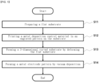
- FIG. 1 is a drawing which shows a flowchart of the 3-dimensional metal electrode patterning method using a metal deposition control material according to the first embodiment of one example of the present invention
- FIG. 2 is a drawing which shows a flowchart of the 3-dimensional metal electrode patterning method using a metal deposition control material according to the second embodiment of one example of the present invention.
- the 3-dimensional metal electrode patterning method according to the present invention starts from a conventionally known deposition technology which evaporates a metal source through heat or other energy supply, and deposits the evaporated metal particle in a gas state on the surface of a substrate to form a conductive metal pattern.
- This vacuum deposition is a method of coating a thin film by evaporating a metal source to be deposited into a gas state in a chamber in a high vacuum state, and is widely used for forming metal wiring for electrical and electronic circuits, or forming OLED light emitting devices for displays and electrodes of semiconductor devices.
- a metal thin film when a metal thin film is formed using vacuum deposition, not only can a pure metal thin film with excellent surface roughness and high conductivity be coated, but also can an extremely thin thickness at a level of several nm be formed, and thus, it can be used even for implementing electrodes with high transmittance.
- the 3-dimensional metal electrode patterning method using a metal deposition control material according to one example of the present invention is that this conventional vacuum deposition technology is further improved, and it can form a 3-dimensional conductive metal pattern on a substrate without the use of a separate mask through a method of coating a material which can control growth of a metal deposition thin film, and at the same time, has intrinsically high stretchability.
- the 3-dimensional metal electrode patterning method using a metal deposition control material comprises preparing a flat substrate (S11); printing a metal deposition control material in an engraved pattern on the flat substrate (S12); forming a 3-dimensional curved substrate by deforming the flat substrate by thermoforming or vacuum forming (S13); and forming a metal electrode pattern by exposing the 3-dimensional curved substrate to metal vapor in a high-vacuum state without a mask (S14).
- a flat substrate is prepared (S11). It is preferable that the flat substrate used in the first embodiment of the present invention has thermoplastic properties so that it can be easily deformed through thermoforming or vacuum forming in a subsequent process.
- the material of the flat substrate may comprise polyethylene terephthalate (PET), polyethylene terephthalate Glycol (PETG) or poly carbonate (PC).
- a metal deposition control material is printed in an engraved pattern on the flat substrate (S12).
- the metal deposition control material may comprise a polymer material which comprises a fluorine functional group and has low surface energy.
- the polymer material used as the metal deposition control material may comprise elastomeric Poly(vinylidene fluoride-co-hexafluoropropylene) (e-PVDF-HFP).
- the printing method of the metal deposition control material is not particularly limited, but it is preferable to apply it using a solution process, and for this, it may be manufactured in a transparent ink form.
- the metal deposition control material should have intrinsically high stretchability, and specifically, it is preferably a material which can maintain a film form without breaking even in a tensile strain range of 1000%.
- the metal deposition control material preferably consists of a material exhibiting a tensile stress of less than 0.4 MPa in a tensile strain range of 0% to 800%.
- the metal deposition control material may comprise various solvents such as N-methyl-2-pyrrolidone (NMP), Triethyl phosphate (TEP), Dimethyl sulfoxide (DMSO), Methyl isobutyl ketone (MIBK), Propylene glycol methyl ether acetate (PGMEA), and the like.
- NMP N-methyl-2-pyrrolidone
- TEP Triethyl phosphate
- DMSO Dimethyl sulfoxide
- MIBK Methyl isobutyl ketone
- PGMEA Propylene glycol methyl ether acetate
- the metal deposition control material may further comprise a crosslinking agent to secure mechanical flexibility of the printed pattern.
- the crosslinking agent may be one selected from the group consisting of TAIC (1,3,5-Triallyl-1,3,5-triazinane-2,4,6-trione, BPO (dibenzoyl peroxide), DCP (Dicumyl peroxide), PBP (Perbutyl peroxide), MIKP (Methyl isobutyl ketone peroxide), and dimethyl Di-t-butylperoxy hexane or a mixture thereof.
- the composition ratio of the metal deposition control material may consist of e-PVDF-HFP of 1 to 50 wt%, a crosslinking agent of 0.05 to 3 wt%, and the remainder solvent.
- the metal deposition control material may be applied using various printing equipment (for example, inkjet printer, pneumatic dispenser, EHD printer), and may be printed to form a certain pattern in an ink form using a printing process.
- the metal deposition control material may be applied using a roll-to-roll coating method.
- the region in which the metal deposition control material is printed on a substrate does not form a metal thin film as the deposition rate is inhibited, so ink application is conducted by patterning the part other than the part in which the metal pattern is to be deposited in an engraved form.
- the thickness of the applied film is at a level inside and outside of several nm ⁇ 10 ⁇ m, and the applied ink may be used after heat treatment at a room temperature ⁇ 180°C, preferably, 100°C to 150°C.
- a 3-dimensional curved substrate is formed by deforming the flat substrate by thermoforming or vacuum forming (S13).
- Metal deposition is performed in a high vacuum, preferably, under a pressure of less than 10 -6 Torr, by moving the 3-dimensional curved substrate, which has the metal deposition control material applied, and at the same time, is deformed through thermoforming or vacuum forming, to a vacuum deposition chamber.
- metal deposition may be performed by Physical Vapor Deposition (PVD).
- PVD Physical Vapor Deposition
- the metal is selectively deposited only in the region in which the metal deposition control material is not applied, even if a separate mask is not used, and patterning is possible without applying an additional wet process.
- a 3-dimensional curved substrate is prepared (S23), and the engraved pattern on the carrier substrate is transferred on the 3-dimensional curved surface by a transferring process (S24).
- the method of forming the 3-dimensional curved substrate to be prepared in the second embodiment is not particularly limited.
- the 3-dimensional curved substrate may be manufactured by deforming a flat substrate by thermoforming or vacuum forming.
- FIG. 4 is a drawing that illustrates the substrate having the 3-dimensional metal electrode pattern according to another example of the present invention, and this substrate was manufactured using the 3-dimensional metal electrode patterning method according to the first embodiment of the present invention.
- the layer thickness of the metal deposition control material region varies partially depending on the deformed form of the substrate, and for example, the larger the curvature of the 3-dimensional curved surface, the more the metal deposition control material region increases, and therefore, the layer thickness becomes thinner.
Landscapes
- Chemical & Material Sciences (AREA)
- Engineering & Computer Science (AREA)
- Chemical Kinetics & Catalysis (AREA)
- Materials Engineering (AREA)
- Mechanical Engineering (AREA)
- Metallurgy (AREA)
- Organic Chemistry (AREA)
- Manufacturing & Machinery (AREA)
- Microelectronics & Electronic Packaging (AREA)
- Physics & Mathematics (AREA)
- General Physics & Mathematics (AREA)
- Physical Vapour Deposition (AREA)
Abstract
Description
- The present invention relates to a 3-dimensional metal electrode patterning method using a metal deposition control material and a substrate having a 3-dimensional metal electrode pattern manufactured by the same, and more specifically, it relates to a method capable of patterning a 3-dimensional metal electrode without a conventionally commonly used rigid shadow or photo mask and a substrate manufactured by the same.
- A method of forming a conductive metal pattern using vacuum deposition is a technology widely used in various fields such as metal wiring for electrical and electronic circuits, OLED light emitting devices for displays and electrodes of semiconductor devices and the like. The most common method of forming a conductive metal pattern using vacuum deposition is a method of using a metal mask, which is, generally, a method of physically removing metals from the part where a pattern is to be formed by processing an alloy with a low thermal expansion coefficient, to prepare a metal mask, and through the part removed of this mask, selectively depositing an electrode.
- Conventional electronic circuits and devices had morphological constraints that they should be made on a flat surface. However, as electronic circuits and devices can be recently implemented also on a 3-dimensional curved surface together with development of flexible and stretchable materials, attempts have been made to implement devices on substrates with various curvatures.
- Metal, a material mainly used as an electrode, is a representative conductive material exhibiting high conductivity, and optical properties that can be adjusted from translucency to reflection. Even sufficiently thin metal thin film has mechanical durability in some degree, and therefore, it can be used also as a flexible electrode, but a problem that cracks are generated at a strain of about 2% to lead electrical defects is known. Thus, in case of the method of forming a metal electrode on a flat substrate first and deforming the substrate, there is a limitation in that it can only be applied within a curvature range that does not cause defects in the metal electrode. In particular, in case of a non-developable surface (for example, sphere, saddle, etc.) of which Gaussian curvature is not 0, a tensile strain is essential to completely cover an electrode sheet along the surface, so self-stretchability of the electrode is required, and as described above, the metal electrode is difficult to apply because they are vulnerable to tension.
- In order to solve such problems, a method of forming a conductive pattern on the curved surface of a substrate directly, rather than a method of deforming an electrode according to a curved substrate, has been attempted. However, for patterning, a rigid shadow mask or photo mask or the like should be used, but such masks are difficult to apply to a curved substrate. As a method to exclude the use of a rigid mask, research of developing a flexible and deformable photo mask or shadow mask has also been reported, but since a subsequent process of removing the mask and leaving only a necessary metal thin film is required after a deposition process, there is a limit to increase in process complexity.
- (Patent document 1)
Korean Laid-open Publication No. 10-2018-0024969 - The present invention is to solve the afore-mentioned problems of the prior art, and an object is to provide a 3-dimensional metal electrode patterning method that can pattern a metal electrode pattern directly on a 3-dimensional curved substrate without a mask in a deposition process and a substrate having a 3-dimensional metal electrode pattern manufactured using the same.
- In order to solve the afore-mentioned problems, the present invention provides a 3-dimensional metal electrode patterning method, comprising preparing a flat substrate; printing a metal deposition control material in an engraved pattern on the flat substrate; forming a 3-dimensional curved substrate by deforming the flat substrate by thermoforming or vacuum forming; and forming a metal electrode pattern by exposing the 3-dimensional curved substrate to metal vapor in a high-vacuum state without a mask, as the first embodiment of one example.
- In addition, the present invention provides a 3-dimensional metal electrode patterning method, comprising preparing a carrier substrate; printing a metal deposition control material in an engraved pattern on the carrier substrate; preparing a 3-dimensonal curved substrate; transferring the engraved pattern on the carrier substrate to the 3-dimensional curved substrate by a transferring process; and forming a metal electrode pattern by exposing the 3-dimensional curved substrate to metal vapor in a high-vacuum state without a mask, as the second embodiment of one example.
- According to one example, the metal deposition control material may comprise e-PVDF-HFP (Elastomeric poly(vinylidene fluoride-co-hexafluoropropylene)).
- According to one example, the metal deposition control material may further comprise a solvent, and the solvent may comprise one selected from the group consisting of NMP (N-methyl-2-pyrrolidone), TEP (Triethyl phosphate), DMSO (Dimethyl sulfoxide), MIBK (Methyl isobutyl ketone), PGMEA (Propylene glycol methyl ether acetate) or a mixture thereof.
- According to one example, the metal deposition control material may further comprise a crosslinking agent, and the crosslinking agent may comprise one selected from the group consisting of TAIC (1,3,5-Triallyl-1,3,5-triazinane-2,4,6-trione, BPO (dibenzoyl peroxide), DCP (Dicumylperoxide), PBP (Perbutyl peroxide), MIKP (Methyl isobutyl ketone peroxide), Dimethyl Di-t-butylperoxy hexane or a mixture thereof.
- According to one example, the pressure in the high-vacuum state when the metal electrode pattern is formed may be 10-6 Torr.
- According to one example, the metal electrode pattern may be formed by a metal or alloy comprising one selected from the group consisting of gold (Au), silver (Ag), magnesium (Mg), copper (Cu), iron (Fe), calcium (Ca) or a combination thereof.
- According to one example, the forming a metal electrode pattern may be performed by Physical Vapor Deposition (PVD).
- According to one example, the metal deposition control material may consist of a material exhibiting a tensile stress of less than 0.4 MPa in a tensile strain range of 0% to 800%.
- According to one example, the flat substrate may have thermoplastic properties.
- According to one example, the thermoforming may be performed in a temperature range of 100°C to 150°C.
- According to one example, the carrier substrate may have surface energy of less than 25 mJ/m2.
- According to one example, the carrier substrate is a PDMS stamp (Polydimethylsiloxane Stamp).
- The present invention provides a substrate having a 3-dimensional metal electrode pattern, comprising a substrate having a 3-dimensional curved surface; a metal electrode pattern formed on at least a part of the 3-dimensional curved surface; a metal deposition control material region formed in a region other than a region in which the metal electrode pattern is formed on the 3-dimensional curved surface; wherein the metal electrode pattern is formed in a constant thickness, and the thickness of the metal deposition control material is formed thinner as the curvature of the 3-dimensional curved surface is larger, as another example.
- According to another example, the metal deposition control material may comprise e-PVDF-HFP.
- According to another example, the metal electrode pattern may be formed by a metal or alloy comprising one selected from the group consisting of gold (Au), silver (Ag), magnesium (Mg), copper (Cu), iron (Fe), calcium (Ca) or a combination thereof.
- According to another example, the metal deposition control material may consist of a material exhibiting a tensile stress of less than 0.4 MPa in a tensile strain range of 0% to 800%.
- According to the composition of the present invention described above, a method capable of patterning a metal thin film electrode which has high electrical conductivity, has low surface roughness, and has a uniform thickness, on a 3-dimensional curved surface without defects, while consisting of a relatively simple process, can be provided.
-
-
FIG. 1 is a flowchart of the 3-dimensional metal electrode patterning method using a metal deposition control material according to the first embodiment of one example of the present invention. -
FIG. 2 is a flowchart of the 3-dimensional metal electrode patterning method using a metal deposition control material according to the second embodiment of one example of the present invention. -
FIG. 3 briefly illustrates each step of the process of the first embodiment of the present invention in chronological order, and (a) shows the step of printing a metal deposition control material in an engraved pattern on a flat substrate, and (b) shows the step of forming a 3-dimensional curved substrate by vacuum forming, and (c) shows the step of forming a metal electrode pattern on the 3-dimensional curved substrate by vacuum deposition. -
FIG. 4 are photographs illustrating the substrate having a 3-dimensional metal electrode pattern actually manufactured using the 3-dimensional metal electrode patterning method according to the present invention, and the left photograph is a photograph showing the 3-dimensional curved substrate formed by thermoforming, and the right photograph is a photograph showing a substrate forming a silver (Ag) electrode on this 3-dimensional curved substrate. -
FIG. 5a shows the substrate having a 3-dimensional metal electrode pattern used in the experiment of the example of the present invention. The 3-dimensional curved shape of the illustrated substrate having a 3-dimensional metal electrode pattern was manufactured with amplitudes of 0 mm, 1 mm, 2 mm, and 5 mm, respectively, in order from the bottom. -
FIG. 5b is a graph showing the result of the experiment of the example of the present invention, and shows the result values of resistance (Ω) and resistance per unit area (Ω·cm-2) according to each amplitude. - Examples of the present disclosure are illustrated for the purpose of describing the technical spirit of the present disclosure. The scope according to the present disclosure are not limited to examples presented below or specific description of these examples.
- All technical terms and scientific terms used in the present disclosure have meanings commonly understood by those skilled in the art to which the present disclosure belongs, unless otherwise defined. All terms used in the present disclosure are selected for the purpose of more clearly describing the present disclosure, and are not selected to limit the scope according to the present invention.
- Expressions such as "comprising", "providing", "having" and the like used in the present disclosure, should be understood in open-ended terms encompassing the possibility of including other examples, unless otherwise stated in a phrase or sentence in which the corresponding expression is included.
- In the present invention, when a part such as a layer, membrane, area, plate and the like is said to be "above" or "on" another part, this includes not only the case in that it is "directly on" another part, but also the case in that there is another part in between. On the contrary, when a part is said to be "right above" another part, it means that there is no other part in between. In addition, that it is said to be "above" or "on" the standard part means being positioned above or below of the standard part, and does not necessarily mean being positioned "above" or "on" the direction opposite to gravity.
- In the present invention, "plane image" refers to the object of the present invention viewed from above, and "cross-sectional image" means the cross section, in which the object of the present invention is vertically cut, viewed from the side.
- Expressions in a singular form described in the present disclosure may include a meaning of a plural form unless otherwise stated, and this is equally applied to expressions in a singular form described in claims.
- Hereinafter, with reference to the accompanied drawings, the examples of the present invention will be described. In this process, the thickness of the lines or sizes of the elements, and the like illustrated in the drawings may be exaggeratedly illustrated for clarity and convenience of description. In addition, in the description of the following examples, describing the same or corresponding elements repeatedly may be omitted. However, even if description of the elements is omitted, it is not intended that such elements are not included in any example.
- In addition, the following examples does not limit the scope of the present invention, but are only illustrative of elements presented in the claims of the present invention, and examples which are included in the technical spirit throughout the description of the present invention and can be replaced as equivalents in the elements of the claims may be included in the scope of the present invention.
-
FIG. 1 is a drawing which shows a flowchart of the 3-dimensional metal electrode patterning method using a metal deposition control material according to the first embodiment of one example of the present invention, andFIG. 2 is a drawing which shows a flowchart of the 3-dimensional metal electrode patterning method using a metal deposition control material according to the second embodiment of one example of the present invention. - The 3-dimensional metal electrode patterning method according to the present invention starts from a conventionally known deposition technology which evaporates a metal source through heat or other energy supply, and deposits the evaporated metal particle in a gas state on the surface of a substrate to form a conductive metal pattern. This vacuum deposition is a method of coating a thin film by evaporating a metal source to be deposited into a gas state in a chamber in a high vacuum state, and is widely used for forming metal wiring for electrical and electronic circuits, or forming OLED light emitting devices for displays and electrodes of semiconductor devices. In particular, when a metal thin film is formed using vacuum deposition, not only can a pure metal thin film with excellent surface roughness and high conductivity be coated, but also can an extremely thin thickness at a level of several nm be formed, and thus, it can be used even for implementing electrodes with high transmittance.
- The 3-dimensional metal electrode patterning method using a metal deposition control material according to one example of the present invention is that this conventional vacuum deposition technology is further improved, and it can form a 3-dimensional conductive metal pattern on a substrate without the use of a separate mask through a method of coating a material which can control growth of a metal deposition thin film, and at the same time, has intrinsically high stretchability.
- Hereinafter, at first, referring to
FIG. 1 , the 3-dimensional metal electrode patterning method using a metal deposition control material according to the first embodiment of one example of the present invention will be described in detail. - Referring to
FIG. 1 , the 3-dimensional metal electrode patterning method using a metal deposition control material according to the first embodiment of the present invention comprises preparing a flat substrate (S11); printing a metal deposition control material in an engraved pattern on the flat substrate (S12); forming a 3-dimensional curved substrate by deforming the flat substrate by thermoforming or vacuum forming (S13); and forming a metal electrode pattern by exposing the 3-dimensional curved substrate to metal vapor in a high-vacuum state without a mask (S14). - At first, a flat substrate is prepared (S11). It is preferable that the flat substrate used in the first embodiment of the present invention has thermoplastic properties so that it can be easily deformed through thermoforming or vacuum forming in a subsequent process. As one non-restrictive example, the material of the flat substrate may comprise polyethylene terephthalate (PET), polyethylene terephthalate Glycol (PETG) or poly carbonate (PC).
- Next, a metal deposition control material is printed in an engraved pattern on the flat substrate (S12).
- The metal deposition control material may comprise a polymer material which comprises a fluorine functional group and has low surface energy. As one non-restrictive example, the polymer material used as the metal deposition control material may comprise elastomeric Poly(vinylidene fluoride-co-hexafluoropropylene) (e-PVDF-HFP). The printing method of the metal deposition control material is not particularly limited, but it is preferable to apply it using a solution process, and for this, it may be manufactured in a transparent ink form.
- The metal deposition control material should have intrinsically high stretchability, and specifically, it is preferably a material which can maintain a film form without breaking even in a tensile strain range of 1000%. In addition, the metal deposition control material preferably consists of a material exhibiting a tensile stress of less than 0.4 MPa in a tensile strain range of 0% to 800%.
- To have physical properties (for example, viscosity, surface tension, boiling point, etc.) suitable for printing equipment, the metal deposition control material may comprise various solvents such as N-methyl-2-pyrrolidone (NMP), Triethyl phosphate (TEP), Dimethyl sulfoxide (DMSO), Methyl isobutyl ketone (MIBK), Propylene glycol methyl ether acetate (PGMEA), and the like.
- In addition, the metal deposition control material may further comprise a crosslinking agent to secure mechanical flexibility of the printed pattern. The crosslinking agent may be one selected from the group consisting of TAIC (1,3,5-Triallyl-1,3,5-triazinane-2,4,6-trione, BPO (dibenzoyl peroxide), DCP (Dicumyl peroxide), PBP (Perbutyl peroxide), MIKP (Methyl isobutyl ketone peroxide), and dimethyl Di-t-butylperoxy hexane or a mixture thereof.
- As one non-restrictive example, the composition ratio of the metal deposition control material may consist of e-PVDF-HFP of 1 to 50 wt%, a crosslinking agent of 0.05 to 3 wt%, and the remainder solvent.
- The metal deposition control material is printed in an engraved pattern on a flat substrate, and then, the metal deposition control material is printed in the part in which a metal electrode pattern should not be formed on the flat substrate. The growth of a deposition thin film is affected by the surface energy of the substrate, and when the cohesion between metal atoms to be deposited is stronger than interaction with the lower substrate, it follows the Volmer-Weber mode in which the film grows in an island form. In addition, a phenomenon that some sources cannot cause a condensation reaction on the surface on which the metal deposition control material is applied and are desorbed occurs complexly, thereby controlling the growth rate of the deposition thin film.
- The metal deposition control material may be applied using various printing equipment (for example, inkjet printer, pneumatic dispenser, EHD printer), and may be printed to form a certain pattern in an ink form using a printing process. As one non-restrictive example, the metal deposition control material may be applied using a roll-to-roll coating method.
- The region in which the metal deposition control material is printed on a substrate does not form a metal thin film as the deposition rate is inhibited, so ink application is conducted by patterning the part other than the part in which the metal pattern is to be deposited in an engraved form. The thickness of the applied film is at a level inside and outside of several nm ~ 10 µm, and the applied ink may be used after heat treatment at a room temperature ~ 180°C, preferably, 100°C to 150°C. The line width of the pattern to be printed is limited by the ink application method of each process equipment, and for example, when an EHD printer is used, it is possible to implement a pattern with a minimum line width at a level of several tens of µm, so even a fine pattern can be printed.
- Then, a 3-dimensional curved substrate is formed by deforming the flat substrate by thermoforming or vacuum forming (S13).
- Since the thermoforming or vacuum forming can be conducted using a conventionally known technology, in the present invention, a specific method for thermoforming or vacuum forming is not particularly limited. For example, a general vacuum forming method which sets a flat substrate on a frame in a vacuum chamber, and heats the flat substrate to make it flexible, and then produces vacuum to adhere the substrate to the frame to form it in a desired form may be used.
- When the flat substrate is deformed by thermoforming or vacuum forming to deform it in a 3-dimensional curved form, the layer or film of the metal deposition control material printed thereon adapts to mechanical deformation, thereby being deformed along the 3-dimensional surface together. As described above, the metal deposition control material used in the present invention consists of a material which can maintain a film form without breaking even in a tensile strain range of 1000%, so despite of mechanical deformation into the 3-dimensional curved substrate, it can maintain the film form along the 3-dimensional surface. However, the degree of deformation is different in each part of the substrate, and the degree of the tensile strain also becomes different depending on the degree of deformation, and due to this, the layer thickness of the metal deposition control material region varies partially. For example, in the part where the curvature of the 3-dimensional curved surface is large, the metal deposition control material region may be greatly expanded, and thus, the total thickness of the metal deposition control material may be thin.
- Finally, a metal electrode pattern is formed on the 3-dimensional curved substrate by exposing it to metal vapor in a high-vacuum state without a mask (S14).
- Metal deposition is performed in a high vacuum, preferably, under a pressure of less than 10-6 Torr, by moving the 3-dimensional curved substrate, which has the metal deposition control material applied, and at the same time, is deformed through thermoforming or vacuum forming, to a vacuum deposition chamber. As one non-restrictive example, metal deposition may be performed by Physical Vapor Deposition (PVD). When deposition is performed on the substrate coated with the metal deposition control material, the metal is selectively deposited only in the region in which the metal deposition control material is not applied, even if a separate mask is not used, and patterning is possible without applying an additional wet process.
- Metal sources used in the deposition process are not particularly limited, and any metal material capable of vacuum deposition may be used in the present invention. As one non-restrictive example, the metal electrode pattern may be formed with a metal or alloy comprising one selected from the group consisting of gold (Au), silver (Ag), magnesium (Mg), copper (Cu), iron (Fe), and calcium (Ca) or a combination thereof.
- Next, referring to
FIG. 2 , the 3-dimensional metal electrode patterning method using a metal deposition control material according to the second embodiment of one example of the present invention will be described in detail. However, for concise description, description of the configuration overlapped with the first embodiment described above will be omitted. - Referring to
FIG. 2 , the 3-dimensional metal electrode patterning method using a metal deposition control material according to the second embodiment of one example of the present invention may comprise preparing a carrier substrate (S21); printing a metal deposition control material in an engraved pattern on the carrier substrate (S22); preparing a 3-dimensional curved substrate (S23); transferring the engraved pattern on the carrier substrate to the 3-dimensional curved substrate by a transferring process (S24); and forming a metal electrode pattern by exposing the 3-dimensional curved substrate to metal vapor in a high-vacuum state without a mask (S25). - At first, a carrier substrate is prepared (S21). It is preferable that the carrier substrate used in the second embodiment of the present invention has low surface energy so that the metal deposition control material can be easily transferred to the substrate with any curved surface in a subsequent transferring process. Further more specifically, the carrier substrate preferably has surface energy of less than 25 mJ/m2. In addition, as one non-restrictive example, the carrier substrate is preferably a PDMS stamp (Polydimethylsiloxane stamp).
- Next, the metal deposition control material is printed in an engraved pattern on the carrier substrate (S22). This step is substantially same as the printing a metal deposition control material in an engraved pattern on the flat substrate of the first embodiment studied above (S12), so the detailed description for this will be omitted.
- After that, a 3-dimensional curved substrate is prepared (S23), and the engraved pattern on the carrier substrate is transferred on the 3-dimensional curved surface by a transferring process (S24). The method of forming the 3-dimensional curved substrate to be prepared in the second embodiment is not particularly limited. As one non-restrictive examples, similarly to the step S13 of the first embodiment studied above, the 3-dimensional curved substrate may be manufactured by deforming a flat substrate by thermoforming or vacuum forming.
- In the transferring process, the carrier substrate, preferably, PDMS stamp is located on the surface of the prepared 3-dimensional curved substrate, and after that, by applying pressure, the metal deposition control material printed in an engraved pattern is transferred on the surface of the 3-dimensional curved substrate. Due to the flexibility of the carrier substrate, the carrier substrate is adhered to the surface of the 3-dimensional curved substrate, and as the carrier substrate has low surface energy, the metal deposition control material may be delivered from the carrier substrate to the surface of the 3-dimensional curved substrate.
- Finally, by exposing the 3-dimensional curved substrate to metal vapor in a high-vacuum state without a mask, a metal electrode pattern is formed (S25). This step is substantially same as the step of forming a metal electrode pattern by exposing the 3-dimensional curved substrate in a high-vacuum state without a mask of the first embodiment studied above (S14), so the detailed description for this will be omitted.
-
FIG. 4 is a drawing that illustrates the substrate having the 3-dimensional metal electrode pattern according to another example of the present invention, and this substrate was manufactured using the 3-dimensional metal electrode patterning method according to the first embodiment of the present invention. - In case of the substrate having the 3-dimensional metal electrode pattern manufactured by the manufacturing method described above, in at least a part of the 3-dimensional curved surface of the substrate, a conductive metal electrode pattern is formed, and in at least other part of the 3-dimensional curved surface, for example, in the region other than the region where the metal electrode pattern is formed, a metal deposition control material region in which the metal deposition control material is applied is formed. As one non-restrictive example, the metal deposition control material region may be formed by printing and drying the metal deposition control material by a printing process. In addition, the conductive metal electrode pattern may be formed by a vacuum deposition process, preferably, PVD process.
- According to the manufacturing method according to the first embodiment or the second embodiment of the present invention described above, the metal deposition control material is formed on the flat substrate or carrier substrate, and then, is deformed to have a 3-dimensional curved surface or is transferred on the 3-dimensional curved surface. The metal deposition control material used in the present invention has stretchability by itself, so it can be deformed along any 3-dimensional curved surface. Therefore, the metal deposition control material formed on the flat substrate is deformed together according to the form of the 3-dimensional curved substrate during thermoforming or vacuum forming of the flat substrate due to self-stretchability. Otherwise, in case of the second embodiment, the metal deposition control material formed on the carrier substrate is tension strained according to the form of the 3-dimensional curved substrate when transferred. At this time, the layer thickness of the metal deposition control material region varies partially depending on the deformed form of the substrate, and for example, the larger the curvature of the 3-dimensional curved surface, the more the metal deposition control material region increases, and therefore, the layer thickness becomes thinner.
- As one non-restrictive example, the metal deposition control material is preferably e-PVDF-HFP. e-PVDF-HFP has advantages that it can maintain the film form without breaking even in a tensile strain range of 1000%, and it can easily deform it along any 3-dimensional curved surface even with little power, as it shows a tensile stress of less than 0.4 MPa in a tensile strain range of 0% to 800%.
- In contrast to the layer of the metal deposition control material, the conductive metal electrode pattern is formed in a substantially constant thickness throughout the substrate, as deposition is achieved after it is deformed into a 3-dimensional curved substrate through thermoforming or vacuum forming. The conductive metal electrode pattern is not particularly limited, but it is preferably formed of a metal or alloy comprising one selected from the group consisting of gold (Au), silver (Ag), magnesium (Mg), cooper (Cu), iron (Fe), and calcium (Ca), or a combination thereof.
- Hereinafter, the effect of the manufacturing method according to one example of the present invention will be described in detail through experimental results.
- At first, by the manufacturing method according to the first embodiment described above, a substrate having a 3-dimensional metal electrode pattern was manufactured. Specifically, the present inventors prepared a polyethylene terephthalate Glycol (PETG) substrate as a substrate and applied a metal deposition control material, and then deformed this substrate into a 3-dimensional curved surface in a sine wave form by vacuum forming. After that, silver (Ag) was deposited in a shape with a width of 10 mm, and a length of 60 mm, under high vacuum of less than 10-6 torr by a PVD process to form a conductive metal electrode.
- The present inventors formed a 3-dimensional curved surface by vacuum forming, and conducted the experiment while changing the amplitude to 0 mm, 1 mm, 2 mm, and 5 mm, respectively.
FIG. 5a shows the actual results manufactured in this experiment. Afterwards, the resistance was measured on both sides of the conductive metal electrode pattern in the longitudinal direction for each substrate, and the results were shown in Table 1 andFIG. 5b .[Table 1] Classification Amplitude (mm) Maximum curvature (mm- 1) Resistance (Ω) Resistance per unit area (Ω·cm-2) Invention example 1 0 0 1.27 0.21 Invention example 2 1 0.1 1.44 0.23 Invention example 3 2 0.2 1.56 0.24 Invention example 4 5 0.5 2.14 0.24 - As a result of the experiment, it could be confirmed that the maximum curvature also became larger (0→0.5mm-1), as the amplitude in a sine wave form increased (0→5mm), but when converted to resistance per unit area of the region where the electrode was formed, the resistance showed similar values at the level of 0.23 ± 0.01 Ω·cm-2 under all amplitude conditions. Through this experiment, it could be confirmed that it is possible to deposit electrodes with uniform thickness on a 3-dimensional curved surface without influence of the curvature according to the manufacturing method according to one example of the present invention.
- The above description of the present invention is merely intended to illustratively describe the technical spirit of the present invention, and various changes and modifications can be made by those skilled in the art without departing from the essential features of the present invention. Therefore, the examples disclosed herein are not intended to limit the technical spirit of the present invention, but are intended to describe the present invention, and the scope of the technical spirit of the present invention is not limited by these examples. The protection scope of the present invention should be construed by the following claims, and all technical spirits within the equivalent scope thereto should be interpreted as being included in the scope of the present invention.
Claims (17)
- A 3-dimensional metal electrode patterning method, comprisingpreparing a flat substrate;printing a metal deposition control material in an engraved pattern on the flat substrate;forming a 3-dimensional curved substrate by deforming the flat substrate by thermoforming or vacuum forming; andforming a metal electrode pattern by exposing the 3-dimensional curved substrate to metal vapor in a high-vacuum state without a mask.
- A 3-dimensional metal electrode patterning method, comprisingpreparing a carrier substrate;printing a metal deposition control material in an engraved pattern on the carrier substrate;preparing a 3-dimensonal curved substrate;transferring the engraved pattern on the carrier substrate to the 3-dimensional curved substrate by a transferring process; andforming a metal electrode pattern by exposing the 3-dimensional curved substrate to metal vapor in a high-vacuum state without a mask.
- The 3-dimensional metal electrode patterning method according to claim 1 or claim 2,
wherein the metal deposition control material comprises e-PVDF-HFP (Elastomeric poly(vinylidene fluoride-co-hexafluoropropylene)). - The 3-dimensional metal electrode patterning method according to claim 3, wherein the metal deposition control material further comprises a solvent, and the solvent comprises one selected from the group consisting of NMP (N-methyl-2-pyrrolidone), TEP (Triethyl phosphate), DMSO (Dimethyl sulfoxide), MIBK (Methyl isobutyl ketone), PGMEA (Propylene glycol methyl ether acetate) or a mixture thereof.
- The 3-dimensional metal electrode patterning method according to claim 4,wherein the metal deposition control material further comprises a crosslinking agent, andthe crosslinking agent comprises one selected from the group consisting of TAIC (1,3,5-Triallyl-1,3,5-triazinane-2,4,6-trione, BPO (dibenzoyl peroxide), DCP (Dicumylperoxide), PBP (Perbutyl peroxide), MIKP (Methyl isobutyl ketone peroxide), Dimethyl Di-t-butylperoxy hexane or a mixture thereof.
- The 3-dimensional metal electrode patterning method according to claim 1 or claim 2,
wherein the pressure in the high-vacuum state is less than 10-6 Torr. - The 3-dimensional metal electrode patterning method according to claim 1 or claim 2,
wherein the metal electrode pattern is formed by a metal or alloy comprising one selected from the group consisting of gold (Au), silver (Ag), magnesium (Mg), copper (Cu), iron (Fe), calcium (Ca) or a combination thereof. - The 3-dimensional metal electrode patterning method according to claim 1 or claim 2,
wherein the forming a metal electrode pattern is performed by Physical Vapor Deposition (PVD). - The 3-dimensional metal electrode patterning method according to claim 1 or claim 2,
wherein the metal deposition control material consists of a material exhibiting a tensile stress of less than 0.4 MPa in a tensile strain range of 0% to 800%. - The 3-dimensional metal electrode patterning method according to claim 1,
wherein the flat substrate has thermoplastic properties. - The 3-dimensional metal electrode patterning method according to claim 1,
wherein the thermoforming is performed in a temperature range of 100°C to 150°C. - The 3-dimensional metal electrode patterning method according to claim 2,
wherein the carrier substrate has surface energy of less than 25 mJ/m2. - The 3-dimensional metal electrode patterning method according to claim 2,
wherein the carrier substrate is a PDMS stamp (Polydimethylsiloxane Stamp). - A substrate having a 3-dimensional metal electrode pattern, comprisinga substrate having a 3-dimensional curved surface;a metal electrode pattern formed on at least a part of the 3-dimensional curved surface;a metal deposition control material region formed in a region other than a region in which the metal electrode pattern is formed on the 3-dimensional curved surface;wherein the metal electrode pattern is formed in a constant thickness, andthe thickness of the metal deposition control material is formed thinner as the curvature of the 3-dimensional curved surface is larger.
- The substrate having a 3-dimensional metal electrode pattern according to claim 14,
wherein the metal deposition control material comprises e-PVDF-HFP. - The substrate having a 3-dimensional metal electrode pattern according to claim 14 or claim 15,
wherein the metal electrode pattern is formed by a metal or alloy comprising one selected from the group consisting of gold (Au), silver (Ag), magnesium (Mg), copper (Cu), iron (Fe), calcium (Ca) or a combination thereof. - The substrate having a 3-dimensional metal electrode pattern according to claim 14 or claim 15,
wherein the metal deposition control material consists of a material exhibiting a tensile stress of less than 0.4 MPa in a tensile strain range of 0% to 800%.
Applications Claiming Priority (2)
| Application Number | Priority Date | Filing Date | Title |
|---|---|---|---|
| KR1020230088330A KR102916413B1 (en) | 2023-07-07 | 2023-07-07 | 3-dimensional metal electrode patterning method using metal deposition control material and substrate having 3-dimensional metal electrode pattern manufactured by the method |
| PCT/KR2024/009176 WO2025014147A1 (en) | 2023-07-07 | 2024-07-01 | Three-dimensional metal electrode patterning method using metal deposition control material, and substrate having three-dimensional metal electrode pattern, manufactured thereby |
Publications (3)
| Publication Number | Publication Date |
|---|---|
| EP4520852A1 true EP4520852A1 (en) | 2025-03-12 |
| EP4520852A4 EP4520852A4 (en) | 2025-09-03 |
| EP4520852B1 EP4520852B1 (en) | 2026-04-15 |
Family
ID=93284126
Family Applications (1)
| Application Number | Title | Priority Date | Filing Date |
|---|---|---|---|
| EP24787044.7A Active EP4520852B1 (en) | 2023-07-07 | 2024-07-01 | Three-dimensional metal electrode patterning method using metal deposition control material |
Country Status (3)
| Country | Link |
|---|---|
| EP (1) | EP4520852B1 (en) |
| KR (1) | KR102916413B1 (en) |
| WO (1) | WO2025014147A1 (en) |
Family Cites Families (8)
| Publication number | Priority date | Publication date | Assignee | Title |
|---|---|---|---|---|
| JP2004349540A (en) * | 2003-05-23 | 2004-12-09 | Seiko Epson Corp | Manufacturing method of thin film device, electro-optical device, and electronic apparatus |
| DE102006037998A1 (en) * | 2006-08-14 | 2008-02-21 | Schreiner Group Gmbh & Co. Kg | Method for producing a three-dimensional component |
| KR100993342B1 (en) * | 2008-09-03 | 2010-11-10 | 삼성전기주식회사 | Printed circuit board and manufacturing method thereof |
| US9793481B2 (en) * | 2008-10-01 | 2017-10-17 | The Regents Of The University Of Michigan | Patterning by stamped metal resist |
| EP2960280A1 (en) | 2014-06-26 | 2015-12-30 | E.T.C. S.r.l. | Photocrosslinkable compositions, patterned high k thin film dielectrics and related devices |
| KR20180024969A (en) | 2016-08-31 | 2018-03-08 | 주식회사 아모센스 | Flexible circuit board manufacturing method and sensor for detecting touch pressure applied flexible circuit board manufactured by the method |
| KR102120040B1 (en) * | 2018-11-01 | 2020-06-10 | 주식회사 라훔나노테크 | Etchingless printing type method for forming micro electrode pattern |
| KR102740028B1 (en) * | 2021-12-03 | 2024-12-06 | 서울대학교산학협력단 | Metal Electrode Patterning Method Using Pattern formation Control Material and Substrate, Display and Electronic Device Having Metal Electrode Pattern |
-
2023
- 2023-07-07 KR KR1020230088330A patent/KR102916413B1/en active Active
-
2024
- 2024-07-01 WO PCT/KR2024/009176 patent/WO2025014147A1/en not_active Ceased
- 2024-07-01 EP EP24787044.7A patent/EP4520852B1/en active Active
Also Published As
| Publication number | Publication date |
|---|---|
| KR102916413B1 (en) | 2026-01-22 |
| WO2025014147A1 (en) | 2025-01-16 |
| EP4520852B1 (en) | 2026-04-15 |
| KR20250008261A (en) | 2025-01-14 |
| EP4520852A4 (en) | 2025-09-03 |
Similar Documents
| Publication | Publication Date | Title |
|---|---|---|
| US10723112B2 (en) | Method of transferring thin film | |
| US8631759B2 (en) | System and method for depositing thin layers on non-planar substrates by stamping | |
| EP2599621A1 (en) | Gas barrier film, process for production of gas barrier film, and electronic device | |
| KR102257729B1 (en) | Laminated film, and method for manufacturing composite film | |
| WO2016010106A1 (en) | Thin substrate, method for manufacturing same, and method for transporting substrate | |
| JP3763710B2 (en) | Wafer support with dustproof cover film and manufacturing method thereof | |
| WO2018021089A1 (en) | Gas barrier film, solar cell, and method for manufacturing gas barrier film | |
| KR102740028B1 (en) | Metal Electrode Patterning Method Using Pattern formation Control Material and Substrate, Display and Electronic Device Having Metal Electrode Pattern | |
| EP4520852B1 (en) | Three-dimensional metal electrode patterning method using metal deposition control material | |
| JP6520133B2 (en) | Laminate, method of manufacturing conductive substrate using the same, and method of manufacturing electronic device | |
| EP2242341B1 (en) | Process for producing structure with metal film, mother die for use in the process, and structure produced by the process | |
| US20080038482A1 (en) | Method for Low Temperature Production of Nano-Structured Iron Oxide Coatings | |
| CN1886031A (en) | Method for forming fine patterns using soft mold | |
| TW201805158A (en) | Laminated body and protective film | |
| JP2017188204A (en) | Thin substrate, method for manufacturing the same, and method for peeling substrate | |
| KR102951611B1 (en) | Template for metal electrode patterning, stretchable metal electrode using the same and manufacturing method thereof | |
| US20240224770A1 (en) | Metal electrode patterning method using pattern formation control material and substrate, electronic device and display having metal electrode pattern | |
| KR101939170B1 (en) | Composite sheet with thermal and electric conductivity | |
| WO2018180961A1 (en) | Transparent conductive laminate and production method therefor | |
| CN1511185A (en) | Adhesive silicone rubber with release properties | |
| JP6913941B2 (en) | Stamper for forming a pattern structure, its manufacturing method, and a manufacturing method of a pattern structure | |
| JP2016072132A (en) | Pattern forming method and pattern forming substrate | |
| JP2004058049A (en) | Film formation method | |
| JP2005264254A (en) | Metal vapor deposition film, metal vapor deposition body provided with the metal vapor deposition film, and manufacturing method thereof | |
| JP2011005677A (en) | Transfer sheet |
Legal Events
| Date | Code | Title | Description |
|---|---|---|---|
| STAA | Information on the status of an ep patent application or granted ep patent |
Free format text: STATUS: UNKNOWN |
|
| STAA | Information on the status of an ep patent application or granted ep patent |
Free format text: STATUS: THE INTERNATIONAL PUBLICATION HAS BEEN MADE |
|
| PUAI | Public reference made under article 153(3) epc to a published international application that has entered the european phase |
Free format text: ORIGINAL CODE: 0009012 |
|
| STAA | Information on the status of an ep patent application or granted ep patent |
Free format text: STATUS: REQUEST FOR EXAMINATION WAS MADE |
|
| 17P | Request for examination filed |
Effective date: 20241017 |
|
| AK | Designated contracting states |
Kind code of ref document: A1 Designated state(s): AL AT BE BG CH CY CZ DE DK EE ES FI FR GB GR HR HU IE IS IT LI LT LU LV MC ME MK MT NL NO PL PT RO RS SE SI SK SM TR |
|
| A4 | Supplementary search report drawn up and despatched |
Effective date: 20250805 |
|
| RIC1 | Information provided on ipc code assigned before grant |
Ipc: C23C 14/14 20060101AFI20250730BHEP Ipc: C23C 14/02 20060101ALI20250730BHEP Ipc: C23C 14/04 20060101ALI20250730BHEP Ipc: C23C 14/24 20060101ALI20250730BHEP Ipc: H10K 71/60 20230101ALI20250730BHEP Ipc: H10K 71/00 20230101ALI20250730BHEP Ipc: H10K 77/10 20230101ALI20250730BHEP |
|
| REG | Reference to a national code |
Ref country code: DE Ref legal event code: R079 Ipc: H10K0071000000 Ref country code: DE Ref legal event code: R079 Ref document number: 602024004031 Country of ref document: DE Free format text: PREVIOUS MAIN CLASS: C23C0014140000 Ipc: H10K0071000000 |
|
| GRAP | Despatch of communication of intention to grant a patent |
Free format text: ORIGINAL CODE: EPIDOSNIGR1 |
|
| STAA | Information on the status of an ep patent application or granted ep patent |
Free format text: STATUS: GRANT OF PATENT IS INTENDED |
|
| RIC1 | Information provided on ipc code assigned before grant |
Ipc: H10K 71/00 20230101AFI20251105BHEP Ipc: H10K 71/60 20230101ALI20251105BHEP Ipc: H10K 77/10 20230101ALI20251105BHEP Ipc: C23C 14/14 20060101ALI20251105BHEP Ipc: C23C 14/02 20060101ALI20251105BHEP Ipc: C23C 14/04 20060101ALI20251105BHEP Ipc: C23C 14/24 20060101ALI20251105BHEP Ipc: C23C 14/20 20060101ALI20251105BHEP Ipc: G03F 7/00 20060101ALI20251105BHEP Ipc: H05K 3/00 20060101ALI20251105BHEP Ipc: H05K 3/10 20060101ALI20251105BHEP Ipc: H05K 3/14 20060101ALI20251105BHEP |
|
| DAV | Request for validation of the european patent (deleted) | ||
| DAX | Request for extension of the european patent (deleted) | ||
| INTG | Intention to grant announced |
Effective date: 20251113 |
|
| GRAS | Grant fee paid |
Free format text: ORIGINAL CODE: EPIDOSNIGR3 |
|
| GRAA | (expected) grant |
Free format text: ORIGINAL CODE: 0009210 |
|
| STAA | Information on the status of an ep patent application or granted ep patent |
Free format text: STATUS: THE PATENT HAS BEEN GRANTED |
|
| AK | Designated contracting states |
Kind code of ref document: B1 Designated state(s): AL AT BE BG CH CY CZ DE DK EE ES FI FR GB GR HR HU IE IS IT LI LT LU LV MC ME MK MT NL NO PL PT RO RS SE SI SK SM TR |
|
| REG | Reference to a national code |
Ref country code: CH Ref legal event code: F10 Free format text: ST27 STATUS EVENT CODE: U-0-0-F10-F00 (AS PROVIDED BY THE NATIONAL OFFICE) Effective date: 20260415 |
|
| REG | Reference to a national code |
Ref country code: DE Ref legal event code: R096 Ref document number: 602024004031 Country of ref document: DE |