EP4517848A1 - Light-emitting device - Google Patents
Light-emitting device Download PDFInfo
- Publication number
- EP4517848A1 EP4517848A1 EP23826957.5A EP23826957A EP4517848A1 EP 4517848 A1 EP4517848 A1 EP 4517848A1 EP 23826957 A EP23826957 A EP 23826957A EP 4517848 A1 EP4517848 A1 EP 4517848A1
- Authority
- EP
- European Patent Office
- Prior art keywords
- emitting device
- frame body
- lead
- light
- recess
- Prior art date
- Legal status (The legal status is an assumption and is not a legal conclusion. Google has not performed a legal analysis and makes no representation as to the accuracy of the status listed.)
- Pending
Links
Images






Classifications
-
- H—ELECTRICITY
- H10—SEMICONDUCTOR DEVICES; ELECTRIC SOLID-STATE DEVICES NOT OTHERWISE PROVIDED FOR
- H10H—INORGANIC LIGHT-EMITTING SEMICONDUCTOR DEVICES HAVING POTENTIAL BARRIERS
- H10H20/00—Individual inorganic light-emitting semiconductor devices having potential barriers, e.g. light-emitting diodes [LED]
- H10H20/80—Constructional details
- H10H20/85—Packages
- H10H20/857—Interconnections, e.g. lead-frames, bond wires or solder balls
-
- H—ELECTRICITY
- H10—SEMICONDUCTOR DEVICES; ELECTRIC SOLID-STATE DEVICES NOT OTHERWISE PROVIDED FOR
- H10H—INORGANIC LIGHT-EMITTING SEMICONDUCTOR DEVICES HAVING POTENTIAL BARRIERS
- H10H20/00—Individual inorganic light-emitting semiconductor devices having potential barriers, e.g. light-emitting diodes [LED]
- H10H20/01—Manufacture or treatment
- H10H20/036—Manufacture or treatment of packages
- H10H20/0364—Manufacture or treatment of packages of interconnections
-
- H—ELECTRICITY
- H10—SEMICONDUCTOR DEVICES; ELECTRIC SOLID-STATE DEVICES NOT OTHERWISE PROVIDED FOR
- H10H—INORGANIC LIGHT-EMITTING SEMICONDUCTOR DEVICES HAVING POTENTIAL BARRIERS
- H10H20/00—Individual inorganic light-emitting semiconductor devices having potential barriers, e.g. light-emitting diodes [LED]
- H10H20/80—Constructional details
- H10H20/85—Packages
- H10H20/8506—Containers
-
- H—ELECTRICITY
- H10—SEMICONDUCTOR DEVICES; ELECTRIC SOLID-STATE DEVICES NOT OTHERWISE PROVIDED FOR
- H10H—INORGANIC LIGHT-EMITTING SEMICONDUCTOR DEVICES HAVING POTENTIAL BARRIERS
- H10H20/00—Individual inorganic light-emitting semiconductor devices having potential barriers, e.g. light-emitting diodes [LED]
- H10H20/80—Constructional details
- H10H20/85—Packages
- H10H20/852—Encapsulations
- H10H20/853—Encapsulations characterised by their shape
Definitions
- the present invention relates to a light-emitting device, and more particularly to a light-emitting device having a semiconductor light-emitting element such as a light-emitting diode (LED) mounted on a lead frame.
- a semiconductor light-emitting element such as a light-emitting diode (LED) mounted on a lead frame.
- Patent Literature 1 discloses a method for forming a light-emitting device by forming a resin molded body on a lead frame provided with notches, and cutting the resin molded body and the lead frame along the notches.
- Patent Literature 2 discloses a surface-mounted light-emitting device having a first resin molded body composed of a light-emitting element and a first and a second leads, which are integrally molded, and a second resin molded body containing a phosphor coating the light-emitting element.
- the present invention has been made in view of the problem described above, and an object of the invention is to provide a light-emitting device that prevents peeling between a resin and a lead frame, exhibits high die shear strength, and is less susceptible to defects such as wire breakage.
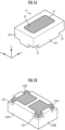
- FIG. 1A and FIG. 1B are conceptual diagrams illustrating an essential section of a light-emitting device 10 according to a first embodiment of the present invention, and are perspective views of the essential section observed from the upper surface side and the lower surface side, respectively.
- the light-emitting device 10 has a plurality of lead electrodes (hereinafter also referred to simply as "the leads") and a resin frame body 22. The following will describe a case where the light-emitting device 10 has two leads 12A and 12B; however, the light-emitting device 10 may have three or more leads.
- the resin frame body 22 has an opening 25 in which a light-emitting element is installed, and the opening 25 is filled with the coating member 35.
- the four corners on the back surface of the light-emitting device 10 have recesses 23 where the corners of the leads 12A and 12B are exposed inside.
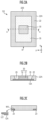
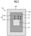
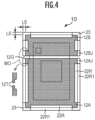
- FIG. 2A is a diagram illustrating the upper surface of the light-emitting device 10, and FIG. 2B is a sectional view taken along line A-A illustrated in FIG. 2A . Further, FIG. 2C is a side view observed from direction B illustrated in FIG. 2A . Further, FIG. 3 is a diagram illustrating the upper surface of the light-emitting device 10 before being filled with the coating member 35, and FIG. 4 is a diagram illustrating the back surface (the surface to be mounted on a circuit board) of the light-emitting device 10.
- the light-emitting device 10 has the lead 12A (first electrode) and the lead 12B (second electrode), which have plate shapes.
- the core material of the lead 12A and the lead 12B is made of copper (Cu), which is a metal that has good etching properties (corrosive properties), and the surface thereof is plated with nickel/gold (Ni/Au), which is a corrosion-resistant metal.
- Aluminum (Al), which is a corrosive metal, or an iron alloy such as iron-nickel-cobalt (Fe-Ni-Co) can be used as the core material of the lead 12A and the lead 12B.
- a corrosion-resistant metal such as platinum (Pt), palladium (Pd), or rhodium (Rh) can be used for the surfaces of the lead 12A and the lead 12B.
- a lead pair 12 consisting of the leads 12A and 12B (hereinafter also referred to as a lead frame 12 of the light-emitting device 10) is formed on substantially the same surface and separated from each other by a gap (slit) 12G between the leads 12A and 12B.
- the lead 12A and the lead 12B will be referred to simply as the leads when there is no particular distinction therebetween.
- the resin frame body 22 is formed by, for example, adding titanium oxide particles to a silicone resin, an epoxy resin, or an acrylic resin (white resin).
- the resin frame body 22 may be formed by adding carbon black to a silicone resin, an epoxy resin, or an acrylic resin (black resin).
- the resin frame body 22 has a rectangular shape (rectangular columnar shape) and has two outer side surfaces 22A parallel to each other and two outer side surfaces 22B perpendicular to the outer side surfaces 22A.
- the four corners of the back surface of the resin frame body 22 have the recesses 23 in which the corners of the leads 12A and 12B are exposed inside.
- thinner portions 12T are provided at outer edge portions WS of the leads 12A and 12B excluding the corners.
- thinner portions 12T are provided at edge portions WO where the leads 12A and 12B face each other. The thinner portions 12T cover the edges of the leads 12A and 12B by the resin of the resin frame body 22, thus preventing the leads from peeling off from the resin frame body 22 during dicing or the like.
- the thinner portions 12T are formed by so-called half etching to a depth of, for example, approximately 50% relative to the thickness of the leads 12A and 12B.
- the light-emitting device 10 is mounted by placing the back surface of the light-emitting device 10 (i.e., the back surface of the resin frame body 22) on a circuit board or the like, and attaching by using solder or the like. As illustrated in FIG. 1B and FIG. 4 , the recesses 23 are provided at the four corners of the back surface (mounting surface) of the resin frame body 22.
- the resin frame body 22 is provided so as to enclose the entire outer peripheries of the leads, burying the gap between the leads. The end portions of the leads are exposed in the recesses 23.
- FIG. 5 is a partial enlarged perspective view of the recess 23 in an enlarged view.
- the resin frame body 22 is recessed from the outer side surfaces 22A and 22B, and the rectangular corner of the lead 12A is exposed in the recess 23.
- the recess 23 in which the corner of the lead 12A is exposed will be described. The same applies to the recess 23 in which the corner of the lead 12B is exposed.
- an end surface 12E of the corner of the lead 12A is located in a position recessed inward from the outer side surfaces 22A and 22B of the resin frame body 22.
- the resin frame body 22 has a rectangular (L-shaped) bottom surface 22H, and the end surface 12E of the lead 12A is located in a position recessed inward from the outer side surfaces 22A and 22B by a distance LS ( FIG. 4 ).
- fillet guards 22G are formed as the partition walls of the resin frame body 22.
- a rectangular space for accommodating a solder fillet is defined in the recess 23 by the fillet guards 22G and the bottom surface 22H of the resin frame body 22.
- the recess 23 functions as a rectangular housing for accommodating the solder fillet.
- the depths (heights) of the bottom surface 22H and the fillet guards 22G are substantially the same as the thickness of the lead 12A.
- an outer peripheral portion 22R1 of a back surface 22R of the resin frame body 22 is formed slightly lower than the back surface 22R by the process and has a step 22S with respect to the back surface 22R, as illustrated in FIG. 4 and FIG. 5 .
- the light-emitting device 10 can be mounted without being detached from the circuit board.
- it is possible to achieve mounting with high die shear strength and without impairing heat dissipation and reliability.
- the back surface 22R of the resin frame body 22 may be a flat surface without the step 22S.
- the recess 23 may be formed by removing only the surface layer (plating layer) of the lead frame 12 by a micro milling cutter or the like such that the step 22S is not formed.
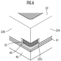
- FIG. 6 is a partial enlarged perspective view illustrating a solder joint in an enlarged view when the light-emitting device 10 is mounted on the wiring (land) 41 of the circuit board 40 by using the solder 45.
- the fillet of the solder 45 is formed in the recess 23, thus making it possible to maintain high die shear strength also in the case of mounting the light-emitting device 10 on the wiring that is approximately the same size therewith.
- FIG. 7 is a partial enlarged perspective view illustrating, in an enlarged view, the recess 23, which is a modified example of the present embodiment.
- the recess 23 having an arc shape (fan-like shape) is formed.
- the bottom surface 22H of the resin frame body 22 has an arc shape (or a quadrant shape), and the end surface (side surface) 12E of the end portion of the lead 12A has a cylindrical side surface shape.
- the fillet guards 22G which are the partition walls extending and protruding from the resin frame body 22, are formed on both sides of the end portion of the lead 12A.
- a quarter-cylindrical space for accommodating the solder fillet is defined in the recess 23 by the fillet guards 22G and the bottom surface 22H of the resin frame body 22.
- the arc-shaped recess 23 functions as a housing for accommodating the solder fillet.
- the above-described protruding fillet guards 22G hold a part of the solder fillet in a necking manner, thus making it possible to increase the die shear strength.
- the fillet of the solder 45 is formed in the recess 23, so that high die shear strength can be maintained even when mounting the light-emitting device 10 on wiring of approximately the same size as the light-emitting device 10.
- the recesses 23 of the resin frame body 22 are rectangular and arc-shaped recesses, but the recesses 23 of other shapes may be formed as long as the recesses have the end surfaces of the leads exposed therein and have spaces for accommodating the solder fillets to be connected to the lead end surfaces.
- the resin frame body 22 has the opening 25 (first opening), which is an inner region of the frame body, and the surfaces of the lead 12A and the lead 12B are partly exposed through the opening 25.
- a semiconductor light-emitting element (hereinafter referred to simply as the light-emitting element) 30 is installed in the opening 25.
- the light-emitting element 30 in the present embodiment is composed of an LED (Light Emitting Diode) 31, which is a light source element, and a phosphor 32, which is an optical member provided on the light source element.
- the light source element may alternatively be a laser diode (LD) or the like.
- the optical member is not limited to a phosphor. Further, the optical member may not be provided.
- the lead 12A is an anode electrode
- the lead 12B is a cathode electrode
- a p-electrode of the LED 31 is connected to and placed on the lead 12A
- an n-electrode of the LED 31 is connected to the lead 12B by bonding wire.
- the plate-shaped phosphor 32 is provided on the LED 31.
- the light-emitting element 30 may have an optical member such as a translucent member provided on the LED 31.
- various types of phosphors such as YAG (yttrium aluminum garnet), LuAG (lutetium aluminum garnet), GYAG (gadolinium aluminum garnet), ⁇ , ⁇ sialon, SCASN, CASN, KFS can be appropriately used.
- a nanoparticle light conversion member of a cadmium selenium (CdSn)-based, indium phosphide (InP)-based, or indium nitride (InN)-based member, or the like can be placed on the upper surface (light exit surface) of the LED 31.
- the nanoparticle light conversion member is preferably placed within a hundred and several tens of nm from the upper surface of the LED 31, because the light conversion efficiency is improved by quantum coupling.
- a protection element 33 which is a Zener diode, is mounted by bonding on the lead 12B exposed through the opening 25.
- the other electrode of the protection element 33 is connected to the lead 12A by bonding wire.
- a varistor or the like can be used as the protection element 33. Further, a passive element such as a capacitor, a resistor, or a light receiving element may be provided.
- the resin frame body 22 has a rectangular shape when viewed from above, and has a rectangular columnar opening 25, which is an inner region of the frame body.
- the opening 25 is not limited to the rectangular columnar shape, and may alternatively have a cylindrical shape, a truncated cone shape, or other shape.
- FIG. 8 is a flowchart illustrating the manufacturing method for the light-emitting device 10.
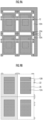
- FIG. 9A to FIG. 9G are top views illustrating steps.
- FIG. 9A, FIG. 9B , and FIG. 9E to FIG. 9G are top views, FIG. 9C and FIG. 9D being back surface views.
- cutting lines CL, along which the devices are divided, are indicated by solid lines, and element mounting portions are indicated by dotted lines.
- a prepared copper (Cu) plate that will become the lead frame 12 is punched by a die to form punched portions 12N ( FIG. 9A ).
- a resist mask may be formed and die-cut by etching.
- a resist mask with openings in the portions that will become the thinner portions 12T is formed before forming the punched portions 12N, and the resist mask is etched to be thinner.
- the upper surface of the lead frame 12 is plated with nickel (Ni) and gold (Au) in this order (Ni/Au plating) by electrolytic plating ( FIG. 9A ).
- the resin frame body 22 of thermosetting resin is formed on the lead frame 12 by insert molding ( FIG. 9B ).
- the resin frame body 22 has the opening 25, which is the inner region of the resin frame body 22, and the surfaces of the lead 12A and the lead 12B are partly exposed through the opening 25.
- FIG. 10A is a schematic top view illustrating an intersectional part X of the cutting lines CL of the lead frame 12 (refer to FIG. 9C and FIG. 9D ) in an enlarged view
- FIG. 10B is a sectional view illustrating the sections of the intersectional part X in step S4 and step S5.
- a plating layer 12P on the surface of the lead frame 12 is removed by dicing (rectangular teeth) along the cutting lines CL at predetermined widths (plating removal portions RB) ( FIG. 10B , top).
- the core material 12C (Cu) is exposed at the plating removal portions RB ( FIG. 9C ).
- the outer peripheral portion 22R1 of the back surface 22R of the resin frame body 22 is also cut to form the step 22S, which is slightly lower than the back surface 22R (refer to FIG. 5 ).
- the plating layer 12P may be removed by milling or the like instead of dicing.
- the core material 12C (Cu) of the lead frame 12 of the plating removal portions is etched using an etching solution ( FIG. 10B , middle).
- the plating layer 12P on the resin frame body 22 is removed by air blasting ( FIG. 10B , bottom).
- Other removal methods include water jet blasting.
- the plating layer 12P on the resin frame body 22 can be left. In such a case, this step is skipped.
- the plating layer 12P that has been left functions as a solder attraction wall when the light-emitting device 10 is soldered to a circuit board.
- the rectangular recess 23 ( FIG. 5 ) is formed at a corner of the resin frame body 22 by etching the lead frame 12 at the intersectional part X ( FIG. 9D ).
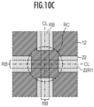
- FIG. 10C illustrates a removal region RC of the lead frame 12 in the case where the recess 23 having the arc shape is formed.
- Gold-tin (Au-Sn) solder paste is printed on the element mounting area. Then, the light-emitting element 30 and the protection element 33 are mounted on the solder.
- Reflow (heating at 300°C) is performed to melt and solidify the gold-tin solder to mount the elements.
- Gold wire is used to perform wire bonding of the light-emitting element 30 and the protection element 33 thereby to mount the elements ( FIG. 9E ).
- Silicone resin which is a translucent adhesive, is applied to the light exit surface of the LED 31.
- the phosphor 32 is mounted on the LED 31.
- temporary curing is performed at 180°C to bond the phosphor 32 ( FIG. 9E ).
- the opening 25 of the resin frame body 22 is filled with a coating resin made of silicone resin containing titanium oxide particles, and the resin is cured by heating at 150°C for three hours to form the coating member 35 ( FIG. 9F ).
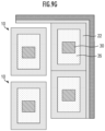
- the light-emitting device 10 is manufactured by the steps described above ( FIG. 9G ).
- a resin frame body may peel off due to a cutting stress applied to the lead frame.
- the lead frame 12 of a cut portion is removed in advance, so that there will be no peeling between the lead frame 12 and the resin frame body 22.
- the present invention can provide a light-emitting device that prevents peeling between a frame body and a lead frame, exhibits high solder joint die shear strength, and is less susceptible to wire breakage and the like.
Landscapes
- Led Device Packages (AREA)
Abstract
Description
- The present invention relates to a light-emitting device, and more particularly to a light-emitting device having a semiconductor light-emitting element such as a light-emitting diode (LED) mounted on a lead frame.
- There has conventionally been known a light-emitting device formed by providing a resin body on a lead frame by insert molding and then cutting the resin body and the lead frame with a dicer.
- For example,
Patent Literature 1 discloses a method for forming a light-emitting device by forming a resin molded body on a lead frame provided with notches, and cutting the resin molded body and the lead frame along the notches. - Further,
Patent Literature 2 discloses a surface-mounted light-emitting device having a first resin molded body composed of a light-emitting element and a first and a second leads, which are integrally molded, and a second resin molded body containing a phosphor coating the light-emitting element. -
- Patent Literature 1:
Japanese Patent Application Laid-Open No. 2010-62272 - Patent Literature 2:
Japanese Patent Application Laid-Open No. 2006-156704 - However, there has been a problem in that cutting integrally molded resin and lead frame causes peeling between the resin and the lead frame, a decrease in die shear strength, broken wires, and the like.
- The present invention has been made in view of the problem described above, and an object of the invention is to provide a light-emitting device that prevents peeling between a resin and a lead frame, exhibits high die shear strength, and is less susceptible to defects such as wire breakage.
- A light-emitting device according to a first embodiment of the present invention is a semiconductor light-emitting device including:
- a plurality of plate-shaped lead electrodes;
- a resin frame body which is provided to enclose an entire outer periphery of the plurality of lead electrodes while burying a gap between the plurality of lead electrodes, and has an opening that exposes the plurality of lead electrodes; and
- a semiconductor light-emitting element mounted on the plurality of lead electrodes exposed through the opening,
- wherein a corner and/or an outer side surface of the frame body has a recess in which an end portion of the lead electrode is exposed at a position set back from the outer side surface of the frame body.
-
-
FIG. 1A is a conceptual diagram illustrating an essential section of a light-emitting device 10 according to a first embodiment of the present invention, and is a perspective view thereof observed from above. -
FIG. 1B is a conceptual diagram illustrating the essential section of the light-emitting device 10 according to the first embodiment of the present invention, and is a perspective view thereof observed from below. -
FIG. 2A is a diagram illustrating an upper surface of the light-emitting device 10. -
FIG. 2B is a sectional view along line A-A illustrated inFIG. 2A . -
FIG. 2C is a side view observed from direction B illustrated inFIG. 2A . -
FIG. 3 is a diagram illustrating the upper surface of the light-emittingdevice 10 before being filled with acoating member 35. -
FIG. 4 is a diagram illustrating the back surface (the surface to be mounted on a circuit board) of the light-emitting device 10. -
FIG. 5 is a partial enlarged perspective view of arecess 23 in an enlarged view. -
FIG. 6 is a partial enlarged perspective view illustrating a solder joint in an enlarged view when the light-emitting device 10 is mounted onwiring 41 of acircuit board 40 by usingsolder 45. -
FIG. 7 is a partial enlarged perspective view illustrating, in an enlarged view, therecess 23 having an arc shape (fan-like shape), which is a modified example of the present embodiment. -
FIG. 8 is a flowchart illustrating a manufacturing method of the light-emitting device 10. -
FIG. 9A is a top view illustrating manufacturing steps S1 and S2 of the light-emitting device 10. -
FIG. 9B is a top view illustrating manufacturing step S3 of the light-emitting device 10. -
FIG. 9C is a top view illustrating manufacturing step S4 of the light-emitting device 10. -
FIG. 9D is a top view illustrating manufacturing step S5 of the light-emitting device 10. -
FIG. 9E is a top view illustrating manufacturing steps S6 and S7 of the light-emitting device 10. -
FIG. 9F is a top view illustrating manufacturing step S8 of the light-emitting device 10. -
FIG. 9G is a top view illustrating manufacturing step S9 of the light-emitting device 10. -
FIG. 10A is a schematic top view illustrating an intersectional part X of alead frame 12 in an enlarged view. -
FIG. 10B is a sectional view illustrating the sections of the intersectional part X in step S4 and step S5. -
FIG. 10C is a diagram illustrating a removal region RC of thelead frame 12 in the case where therecess 23 having an arc shape is formed. - The following will describe preferred embodiments of the present invention, which may be modified or combined as appropriate. In the following description and accompanying drawings, substantially the same or equivalent components will be assigned the same reference numerals.
-
FIG. 1A and FIG. 1B are conceptual diagrams illustrating an essential section of a light-emitting device 10 according to a first embodiment of the present invention, and are perspective views of the essential section observed from the upper surface side and the lower surface side, respectively. The light-emitting device 10 has a plurality of lead electrodes (hereinafter also referred to simply as "the leads") and aresin frame body 22. The following will describe a case where the light-emittingdevice 10 has twoleads device 10 may have three or more leads. - As illustrated in
FIG. 1A , theresin frame body 22 has anopening 25 in which a light-emitting element is installed, and theopening 25 is filled with the coatingmember 35. - As illustrated in
FIG. 1B , the four corners on the back surface of the light-emittingdevice 10 haverecesses 23 where the corners of theleads -
FIG. 2A is a diagram illustrating the upper surface of the light-emittingdevice 10, andFIG. 2B is a sectional view taken along line A-A illustrated inFIG. 2A . Further,FIG. 2C is a side view observed from direction B illustrated inFIG. 2A . Further,FIG. 3 is a diagram illustrating the upper surface of the light-emittingdevice 10 before being filled with the coatingmember 35, andFIG. 4 is a diagram illustrating the back surface (the surface to be mounted on a circuit board) of the light-emittingdevice 10. - The light-emitting
device 10 has thelead 12A (first electrode) and the lead 12B (second electrode), which have plate shapes. The core material of thelead 12A and the lead 12B is made of copper (Cu), which is a metal that has good etching properties (corrosive properties), and the surface thereof is plated with nickel/gold (Ni/Au), which is a corrosion-resistant metal. - Aluminum (Al), which is a corrosive metal, or an iron alloy such as iron-nickel-cobalt (Fe-Ni-Co) can be used as the core material of the
lead 12A and the lead 12B. - Further, a corrosion-resistant metal such as platinum (Pt), palladium (Pd), or rhodium (Rh) can be used for the surfaces of the
lead 12A and the lead 12B. - In the present specification, a
lead pair 12 consisting of theleads lead frame 12 of the light-emitting device 10) is formed on substantially the same surface and separated from each other by a gap (slit) 12G between theleads lead 12A and the lead 12B will be referred to simply as the leads when there is no particular distinction therebetween. - The
resin frame body 22 is insert-molded around theleads resin frame body 22 is provided so as to enclose the entire outer periphery of the leads while filling the gap between the leads thereby to form a resin package. In other words, the leads are not exposed on an outer side surface of theresin frame body 22 and on a surface substantially the same as the outer side surface. - The
resin frame body 22 is formed by, for example, adding titanium oxide particles to a silicone resin, an epoxy resin, or an acrylic resin (white resin). Alternatively, theresin frame body 22 may be formed by adding carbon black to a silicone resin, an epoxy resin, or an acrylic resin (black resin). - As illustrated in
FIG. 1A and FIG. 1B , theresin frame body 22 has a rectangular shape (rectangular columnar shape) and has twoouter side surfaces 22A parallel to each other and two outer side surfaces 22B perpendicular to the outer side surfaces 22A. In addition, the four corners of the back surface of theresin frame body 22 have therecesses 23 in which the corners of theleads - As illustrated in
FIG. 2C ,thinner portions 12T are provided at outer edge portions WS of theleads FIG. 4 ,thinner portions 12T are provided at edge portions WO where theleads thinner portions 12T cover the edges of theleads resin frame body 22, thus preventing the leads from peeling off from theresin frame body 22 during dicing or the like. - The
thinner portions 12T are formed by so-called half etching to a depth of, for example, approximately 50% relative to the thickness of theleads - The light-emitting
device 10 is mounted by placing the back surface of the light-emitting device 10 (i.e., the back surface of the resin frame body 22) on a circuit board or the like, and attaching by using solder or the like. As illustrated inFIG. 1B andFIG. 4 , therecesses 23 are provided at the four corners of the back surface (mounting surface) of theresin frame body 22. - Further, as described above, the
resin frame body 22 is provided so as to enclose the entire outer peripheries of the leads, burying the gap between the leads. The end portions of the leads are exposed in therecesses 23. -
FIG. 5 is a partial enlarged perspective view of therecess 23 in an enlarged view. In therecess 23, theresin frame body 22 is recessed from theouter side surfaces lead 12A is exposed in therecess 23. Therecess 23 in which the corner of thelead 12A is exposed will be described. The same applies to therecess 23 in which the corner of the lead 12B is exposed. - More specifically, in the
recess 23, anend surface 12E of the corner of thelead 12A is located in a position recessed inward from theouter side surfaces resin frame body 22. This means that, in therecess 23, theresin frame body 22 has a rectangular (L-shaped)bottom surface 22H, and theend surface 12E of thelead 12A is located in a position recessed inward from theouter side surfaces FIG. 4 ). - Further, on both sides of the corner of the
lead 12A,fillet guards 22G are formed as the partition walls of theresin frame body 22. A rectangular space for accommodating a solder fillet is defined in therecess 23 by thefillet guards 22G and thebottom surface 22H of theresin frame body 22. In other words, therecess 23 functions as a rectangular housing for accommodating the solder fillet. - As will be described later, if the
bottom surface 22H is formed by etching thelead 12A, then the depths (heights) of thebottom surface 22H and thefillet guards 22G are substantially the same as the thickness of thelead 12A. - In the case where the
recess 23 is formed by etching acore material 12C of thelead frame 12, and a milling process or the like for a lead frame surface layer (plating layer) is used in combination with the etching, an outer peripheral portion 22R1 of aback surface 22R of theresin frame body 22 is formed slightly lower than theback surface 22R by the process and has astep 22S with respect to theback surface 22R, as illustrated inFIG. 4 andFIG. 5 . - In this case, even if there is a burr on the lower end of the outer side surfaces of the
resin frame body 22 of the light-emittingdevice 10, the light-emittingdevice 10 can be mounted without being detached from the circuit board. Thus, it is possible to achieve mounting with high die shear strength and without impairing heat dissipation and reliability. - Further, when mounting the light-emitting
device 10 on a wiring pattern of the same size as the light-emittingdevice 10, even if there are burrs on the peripheral edge of the wiring pattern, it is possible to prevent the light-emittingdevice 10 from tilting, thus preventing the optical axis from shifting. - The
back surface 22R of theresin frame body 22 may be a flat surface without thestep 22S. For example, therecess 23 may be formed by removing only the surface layer (plating layer) of thelead frame 12 by a micro milling cutter or the like such that thestep 22S is not formed. -
FIG. 6 is a partial enlarged perspective view illustrating a solder joint in an enlarged view when the light-emittingdevice 10 is mounted on the wiring (land) 41 of thecircuit board 40 by using thesolder 45. - The fillet of the
solder 45 is formed in therecess 23, thus making it possible to maintain high die shear strength also in the case of mounting the light-emittingdevice 10 on the wiring that is approximately the same size therewith. -
FIG. 7 is a partial enlarged perspective view illustrating, in an enlarged view, therecess 23, which is a modified example of the present embodiment. In the present modified example, therecess 23 having an arc shape (fan-like shape) is formed. - More specifically, in the
recess 23, thebottom surface 22H of theresin frame body 22 has an arc shape (or a quadrant shape), and the end surface (side surface) 12E of the end portion of thelead 12A has a cylindrical side surface shape. - Further, the
fillet guards 22G, which are the partition walls extending and protruding from theresin frame body 22, are formed on both sides of the end portion of thelead 12A. A quarter-cylindrical space for accommodating the solder fillet is defined in therecess 23 by thefillet guards 22G and thebottom surface 22H of theresin frame body 22. In other words, the arc-shapedrecess 23 functions as a housing for accommodating the solder fillet. The above-described protrudingfillet guards 22G hold a part of the solder fillet in a necking manner, thus making it possible to increase the die shear strength. - As with the case of the
rectangular recess 23, the fillet of thesolder 45 is formed in therecess 23, so that high die shear strength can be maintained even when mounting the light-emittingdevice 10 on wiring of approximately the same size as the light-emittingdevice 10. - The above has described the cases where the
recesses 23 of theresin frame body 22 are rectangular and arc-shaped recesses, but therecesses 23 of other shapes may be formed as long as the recesses have the end surfaces of the leads exposed therein and have spaces for accommodating the solder fillets to be connected to the lead end surfaces. - In addition, the case has been described, as an example, where the
recesses 23 are provided at the corners of the light-emitting device 10 (i.e., the resin frame body 22); however, the present invention is not limited thereto. For example, the recesses may be provided in the sides of the light-emittingdevice 10. More specifically, referring toFIG. 4 , a joint 12AJ or 12BJ of thelead recess 23 having a rectangular shape (e.g., an I shape). Therefore, therecesses 23 may be provided at the corners and/or the sides of the light-emittingdevice 10. - As illustrated in
FIG. 3 , theresin frame body 22 has the opening 25 (first opening), which is an inner region of the frame body, and the surfaces of thelead 12A and the lead 12B are partly exposed through theopening 25. A semiconductor light-emitting element (hereinafter referred to simply as the light-emitting element) 30 is installed in theopening 25. - The light-emitting
element 30 in the present embodiment is composed of an LED (Light Emitting Diode) 31, which is a light source element, and aphosphor 32, which is an optical member provided on the light source element. However, the light source element may alternatively be a laser diode (LD) or the like. Further, the optical member is not limited to a phosphor. Further, the optical member may not be provided. - More specifically, for example, the
lead 12A is an anode electrode, the lead 12B is a cathode electrode, a p-electrode of theLED 31 is connected to and placed on thelead 12A, and an n-electrode of theLED 31 is connected to the lead 12B by bonding wire. - Further, the plate-shaped
phosphor 32 is provided on theLED 31. Alternatively, the light-emittingelement 30 may have an optical member such as a translucent member provided on theLED 31. Although there is no particular limit to a phosphor, various types of phosphors such as YAG (yttrium aluminum garnet), LuAG (lutetium aluminum garnet), GYAG (gadolinium aluminum garnet), α, β sialon, SCASN, CASN, KFS can be appropriately used. In addition, when an optical member such as a translucent member is included, a nanoparticle light conversion member of a cadmium selenium (CdSn)-based, indium phosphide (InP)-based, or indium nitride (InN)-based member, or the like can be placed on the upper surface (light exit surface) of theLED 31. In particular, the nanoparticle light conversion member is preferably placed within a hundred and several tens of nm from the upper surface of theLED 31, because the light conversion efficiency is improved by quantum coupling. - Further, a
protection element 33, which is a Zener diode, is mounted by bonding on the lead 12B exposed through theopening 25. The other electrode of theprotection element 33 is connected to thelead 12A by bonding wire. - A varistor or the like can be used as the
protection element 33. Further, a passive element such as a capacitor, a resistor, or a light receiving element may be provided. - In the
opening 25 of theresin frame body 22, the space around the light-emittingelement 30 is filled with the coatingmember 35, which is a sealing resin or a coating resin. InFIG. 3 , the coatingmember 35 is not illustrated, since the drawing is for describing the internal structure. Further, the surface of the light-emitting element 30 (i.e., the surface of the phosphor 32) is exposed from the coatingmember 35. - As illustrated in
FIG. 3 , theresin frame body 22 has a rectangular shape when viewed from above, and has arectangular columnar opening 25, which is an inner region of the frame body. Theopening 25 is not limited to the rectangular columnar shape, and may alternatively have a cylindrical shape, a truncated cone shape, or other shape. - The following will describe in detail the manufacturing method for the light-emitting
device 10 by referring to a flowchart and the accompanying drawings. -
FIG. 8 is a flowchart illustrating the manufacturing method for the light-emittingdevice 10. Further,FIG. 9A to FIG. 9G are top views illustrating steps.FIG. 9A, FIG. 9B , andFIG. 9E toFIG. 9G are top views,FIG. 9C and FIG. 9D being back surface views. In each drawing, for the purpose of clarity, cutting lines CL, along which the devices are divided, are indicated by solid lines, and element mounting portions are indicated by dotted lines. - A prepared copper (Cu) plate that will become the
lead frame 12 is punched by a die to form punchedportions 12N (FIG. 9A ). Instead of punching, a resist mask may be formed and die-cut by etching. When forming thethinner portions 12T at the outer edge of thelead frame 12, a resist mask with openings in the portions that will become thethinner portions 12T is formed before forming the punchedportions 12N, and the resist mask is etched to be thinner. - The upper surface of the
lead frame 12 is plated with nickel (Ni) and gold (Au) in this order (Ni/Au plating) by electrolytic plating (FIG. 9A ). - Subsequently, the
resin frame body 22 of thermosetting resin is formed on thelead frame 12 by insert molding (FIG. 9B ). Theresin frame body 22 has theopening 25, which is the inner region of theresin frame body 22, and the surfaces of thelead 12A and the lead 12B are partly exposed through theopening 25. -
FIG. 10A is a schematic top view illustrating an intersectional part X of the cutting lines CL of the lead frame 12 (refer toFIG. 9C and FIG. 9D ) in an enlarged view, andFIG. 10B is a sectional view illustrating the sections of the intersectional part X in step S4 and step S5. - First, a
plating layer 12P on the surface of thelead frame 12 is removed by dicing (rectangular teeth) along the cutting lines CL at predetermined widths (plating removal portions RB) (FIG. 10B , top). Thecore material 12C (Cu) is exposed at the plating removal portions RB (FIG. 9C ). - At this time, the outer peripheral portion 22R1 of the
back surface 22R of theresin frame body 22 is also cut to form thestep 22S, which is slightly lower than theback surface 22R (refer toFIG. 5 ). - The
plating layer 12P may be removed by milling or the like instead of dicing. - Subsequently, the
core material 12C (Cu) of thelead frame 12 of the plating removal portions is etched using an etching solution (FIG. 10B , middle). - Next, the
plating layer 12P on theresin frame body 22 is removed by air blasting (FIG. 10B , bottom). Other removal methods include water jet blasting. Theplating layer 12P on theresin frame body 22 can be left. In such a case, this step is skipped. Theplating layer 12P that has been left functions as a solder attraction wall when the light-emittingdevice 10 is soldered to a circuit board. - The rectangular recess 23 (
FIG. 5 ) is formed at a corner of theresin frame body 22 by etching thelead frame 12 at the intersectional part X (FIG. 9D ). -
FIG. 10C illustrates a removal region RC of thelead frame 12 in the case where therecess 23 having the arc shape is formed. By removing the intersectional part X of thelead frame 12 in a circular shape, therecesses 23 having the end surfaces 12E, which have the shape of cylindrical side surfaces, can be formed at the four corners of the lead (FIG. 7 ). - Gold-tin (Au-Sn) solder paste is printed on the element mounting area. Then, the light-emitting
element 30 and theprotection element 33 are mounted on the solder. - Reflow (heating at 300°C) is performed to melt and solidify the gold-tin solder to mount the elements.
- Gold wire is used to perform wire bonding of the light-emitting
element 30 and theprotection element 33 thereby to mount the elements (FIG. 9E ). - Silicone resin, which is a translucent adhesive, is applied to the light exit surface of the
LED 31. Next, thephosphor 32 is mounted on theLED 31. Then, temporary curing is performed at 180°C to bond the phosphor 32 (FIG. 9E ). - Subsequently, the
opening 25 of theresin frame body 22 is filled with a coating resin made of silicone resin containing titanium oxide particles, and the resin is cured by heating at 150°C for three hours to form the coating member 35 (FIG. 9F ). - Lastly, the singulation is performed by cutting with a dicer into each device. The light-emitting
device 10 is manufactured by the steps described above (FIG. 9G ). - According to the present invention, in the lead frame removal step (S5), the
lead frame 12 is cut by etching, and thelead frame 12 is not cut in the singulation step (S9). - If the lead frames are cut at the time of singulation into individual light-emitting devices, a resin frame body may peel off due to a cutting stress applied to the lead frame. According to the present invention, the
lead frame 12 of a cut portion is removed in advance, so that there will be no peeling between thelead frame 12 and theresin frame body 22. Thus, it is possible to provide a light-emitting device that has high die shear strength and is less susceptible to wire breakage and the like. - As described in detail above, the present invention can provide a light-emitting device that prevents peeling between a frame body and a lead frame, exhibits high solder joint die shear strength, and is less susceptible to wire breakage and the like.
-
- 10: light-emitting device
- 12: lead frame
- 12A, 12B: lead
- 12E: end surface of lead
- 22: resin frame body
- 22A, 22B: outer side surface
- 22G: fillet guard
- 22H: bottom surface of
resin frame body 22 - 22R: back surface of
resin frame body 22 - 22R1: outer peripheral portion of
back surface 22R - 23: recess
- 30: light-emitting element
- 31: LED
- 32: phosphor
- 35: coating member
- 40: circuit board
- 45: solder
- CL: cutting line
- RB: plating removal portion
Claims (8)
- A semiconductor light-emitting device comprising:a plurality of plate-shaped lead electrodes;a resin frame body which is provided to enclose an entire outer periphery of the plurality of lead electrodes while burying a gap between the plurality of lead electrodes, and has an opening that exposes the plurality of lead electrodes; anda semiconductor light-emitting element mounted on the plurality of lead electrodes exposed through the opening,wherein a corner and/or an outer side surface of the frame body has a recess in which an end portion of the lead electrode is exposed therein at a position set back from the outer side surface of the frame body.
- The semiconductor light-emitting device according to Claim 1, wherein the end portion of the lead electrode exposed in the recess has a rectangular shape.
- The semiconductor light-emitting device according to Claim 1, wherein the end portion of the lead electrode exposed in the recess has an arc shape.
- The semiconductor light-emitting device according to Claim 1, wherein the recess has a height equivalent to a thickness of the lead electrode.
- The semiconductor light-emitting device according to Claim 1, wherein a back surface of the resin frame body has an outer peripheral portion that is lower than the back surface of the resin frame body.
- The semiconductor light-emitting device according to Claim 1, wherein a core material of the lead electrode is a corrosive metal, and a surface layer of the lead electrode is a corrosion-resistant metal.
- The semiconductor light-emitting device according to Claim 6, wherein the core material of the lead electrode is a metal that contains any one or more of copper (Cu), aluminum (Al), and iron (Fe), and the surface layer of the lead electrode is a metal that contains any one or more of gold (Au), platinum (Pt), palladium (Pd), and rhodium (Rh).
- The semiconductor light-emitting device according to any one of Claims 1 to 6, wherein the resin frame body has a partition wall that separates the end portion of the lead electrode, which is exposed in the recess, from an outer side surface of the resin frame body.
Applications Claiming Priority (2)
| Application Number | Priority Date | Filing Date | Title |
|---|---|---|---|
| JP2022100686A JP7902032B2 (en) | 2022-06-22 | 2022-06-22 | Light-emitting device |
| PCT/JP2023/020776 WO2023248770A1 (en) | 2022-06-22 | 2023-06-05 | Light-emitting device |
Publications (2)
| Publication Number | Publication Date |
|---|---|
| EP4517848A1 true EP4517848A1 (en) | 2025-03-05 |
| EP4517848A4 EP4517848A4 (en) | 2025-10-01 |
Family
ID=89379631
Family Applications (1)
| Application Number | Title | Priority Date | Filing Date |
|---|---|---|---|
| EP23826957.5A Pending EP4517848A4 (en) | 2022-06-22 | 2023-06-05 | ELECTROLUMINESCENT DEVICE |
Country Status (7)
| Country | Link |
|---|---|
| US (1) | US20250324830A1 (en) |
| EP (1) | EP4517848A4 (en) |
| JP (1) | JP7902032B2 (en) |
| KR (1) | KR20250026176A (en) |
| CN (1) | CN119404618A (en) |
| TW (1) | TW202404919A (en) |
| WO (1) | WO2023248770A1 (en) |
Cited By (1)
| Publication number | Priority date | Publication date | Assignee | Title |
|---|---|---|---|---|
| US20240379926A1 (en) * | 2021-09-24 | 2024-11-14 | Stanley Electric Co., Ltd. | Light-emitting device, and method for producing light-emitting device |
Family Cites Families (7)
| Publication number | Priority date | Publication date | Assignee | Title |
|---|---|---|---|---|
| JP4608294B2 (en) | 2004-11-30 | 2011-01-12 | 日亜化学工業株式会社 | RESIN MOLDED BODY, SURFACE MOUNTED LIGHT EMITTING DEVICE AND METHOD FOR PRODUCING THEM |
| JP5217800B2 (en) | 2008-09-03 | 2013-06-19 | 日亜化学工業株式会社 | Light emitting device, resin package, resin molded body, and manufacturing method thereof |
| JP2013051296A (en) * | 2011-08-31 | 2013-03-14 | Panasonic Corp | Semiconductor device package and method of manufacturing the same, and semiconductor device |
| KR102153619B1 (en) * | 2014-04-04 | 2020-09-09 | 엘지디스플레이 주식회사 | Light emitting diode device array and liquid crystal display using the same |
| JP6260593B2 (en) * | 2015-08-07 | 2018-01-17 | 日亜化学工業株式会社 | Lead frame, package, light emitting device, and manufacturing method thereof |
| TWM558999U (en) * | 2017-12-11 | 2018-04-21 | 長華科技股份有限公司 | Light-emitting package component |
| JP6888709B2 (en) * | 2020-04-09 | 2021-06-16 | 日亜化学工業株式会社 | Manufacturing method of light emitting device and light emitting device |
-
2022
- 2022-06-22 JP JP2022100686A patent/JP7902032B2/en active Active
-
2023
- 2023-06-05 EP EP23826957.5A patent/EP4517848A4/en active Pending
- 2023-06-05 WO PCT/JP2023/020776 patent/WO2023248770A1/en not_active Ceased
- 2023-06-05 KR KR1020247041195A patent/KR20250026176A/en active Pending
- 2023-06-05 US US18/869,060 patent/US20250324830A1/en active Pending
- 2023-06-05 CN CN202380047842.XA patent/CN119404618A/en active Pending
- 2023-06-14 TW TW112122142A patent/TW202404919A/en unknown
Cited By (1)
| Publication number | Priority date | Publication date | Assignee | Title |
|---|---|---|---|---|
| US20240379926A1 (en) * | 2021-09-24 | 2024-11-14 | Stanley Electric Co., Ltd. | Light-emitting device, and method for producing light-emitting device |
Also Published As
| Publication number | Publication date |
|---|---|
| JP2024001800A (en) | 2024-01-10 |
| US20250324830A1 (en) | 2025-10-16 |
| EP4517848A4 (en) | 2025-10-01 |
| KR20250026176A (en) | 2025-02-25 |
| JP7902032B2 (en) | 2026-08-07 |
| TW202404919A (en) | 2024-02-01 |
| CN119404618A (en) | 2025-02-07 |
| WO2023248770A1 (en) | 2023-12-28 |
Similar Documents
| Publication | Publication Date | Title |
|---|---|---|
| CN102142513B (en) | LED package and method for manufacturing same | |
| EP3591721B1 (en) | Light emitting device | |
| JP5869961B2 (en) | Semiconductor light emitting device | |
| JP6336105B2 (en) | Manufacturing of optoelectronic components | |
| JP6337873B2 (en) | Package, package intermediate, light emitting device, and manufacturing method thereof | |
| JP6260593B2 (en) | Lead frame, package, light emitting device, and manufacturing method thereof | |
| WO2003044872A1 (en) | Compound semiconductor light emitting device and its manufacturing method | |
| JP2013247243A (en) | Semiconductor light-emitting device | |
| US20250324830A1 (en) | Light-emitting device | |
| EP4191689A1 (en) | Semiconductor light emitting device | |
| JP6107229B2 (en) | Light emitting device | |
| JP2017130589A (en) | Light-emitting device manufacturing method | |
| US11223000B2 (en) | Method of manufacturing light emitting element mounting base member, method of manufacturing light emitting device using the light emitting element mounting base member, light emitting element mounting base member, and light emitting device using the light emitting element mounting base member | |
| US20240379926A1 (en) | Light-emitting device, and method for producing light-emitting device | |
| US12261252B2 (en) | Light-emitting device and manufacturing method of the same | |
| EP2682993B1 (en) | Molded package for light emitting device and light emitting device using the same | |
| US20250006880A1 (en) | Semiconductor light-emitting device | |
| JP6701711B2 (en) | Light emitting device | |
| JP2024054731A (en) | Semiconductor light emitting device | |
| EP4418336A1 (en) | Light-emitting device and lead frame | |
| KR100303393B1 (en) | Circuit Board Structure of Semiconductor Package and Manufacturing Method Thereof | |
| JP2018160673A (en) | Method for manufacturing package, method for manufacturing package intermediate, and method for manufacturing light-emitting device |
Legal Events
| Date | Code | Title | Description |
|---|---|---|---|
| STAA | Information on the status of an ep patent application or granted ep patent |
Free format text: STATUS: THE INTERNATIONAL PUBLICATION HAS BEEN MADE |
|
| PUAI | Public reference made under article 153(3) epc to a published international application that has entered the european phase |
Free format text: ORIGINAL CODE: 0009012 |
|
| STAA | Information on the status of an ep patent application or granted ep patent |
Free format text: STATUS: REQUEST FOR EXAMINATION WAS MADE |
|
| 17P | Request for examination filed |
Effective date: 20241127 |
|
| AK | Designated contracting states |
Kind code of ref document: A1 Designated state(s): AL AT BE BG CH CY CZ DE DK EE ES FI FR GB GR HR HU IE IS IT LI LT LU LV MC ME MK MT NL NO PL PT RO RS SE SI SK SM TR |
|
| REG | Reference to a national code |
Ref country code: DE Ref legal event code: R079 Free format text: PREVIOUS MAIN CLASS: H01L0033620000 Ipc: H10H0020850000 |
|
| STAA | Information on the status of an ep patent application or granted ep patent |
Free format text: STATUS: EXAMINATION IS IN PROGRESS |
|
| A4 | Supplementary search report drawn up and despatched |
Effective date: 20250829 |
|
| DAV | Request for validation of the european patent (deleted) | ||
| DAX | Request for extension of the european patent (deleted) | ||
| RIC1 | Information provided on ipc code assigned before grant |
Ipc: H10H 20/85 20250101AFI20250825BHEP Ipc: H10H 20/01 20250101ALI20250825BHEP |
|
| 17Q | First examination report despatched |
Effective date: 20250908 |