EP4516973A1 - Substrate with deposited diamond film and method for producing substrate with deposited diamond film - Google Patents
Substrate with deposited diamond film and method for producing substrate with deposited diamond film Download PDFInfo
- Publication number
- EP4516973A1 EP4516973A1 EP23795915.0A EP23795915A EP4516973A1 EP 4516973 A1 EP4516973 A1 EP 4516973A1 EP 23795915 A EP23795915 A EP 23795915A EP 4516973 A1 EP4516973 A1 EP 4516973A1
- Authority
- EP
- European Patent Office
- Prior art keywords
- diamond film
- niobium carbide
- carbide layer
- layer
- niobium
- Prior art date
- Legal status (The legal status is an assumption and is not a legal conclusion. Google has not performed a legal analysis and makes no representation as to the accuracy of the status listed.)
- Pending
Links
Images


Classifications
-
- C—CHEMISTRY; METALLURGY
- C23—COATING METALLIC MATERIAL; COATING MATERIAL WITH METALLIC MATERIAL; CHEMICAL SURFACE TREATMENT; DIFFUSION TREATMENT OF METALLIC MATERIAL; COATING BY VACUUM EVAPORATION, BY SPUTTERING, BY ION IMPLANTATION OR BY CHEMICAL VAPOUR DEPOSITION, IN GENERAL; INHIBITING CORROSION OF METALLIC MATERIAL OR INCRUSTATION IN GENERAL
- C23C—COATING METALLIC MATERIAL; COATING MATERIAL WITH METALLIC MATERIAL; SURFACE TREATMENT OF METALLIC MATERIAL BY DIFFUSION INTO THE SURFACE, BY CHEMICAL CONVERSION OR SUBSTITUTION; COATING BY VACUUM EVAPORATION, BY SPUTTERING, BY ION IMPLANTATION OR BY CHEMICAL VAPOUR DEPOSITION, IN GENERAL
- C23C16/00—Chemical coating by decomposition of gaseous compounds, without leaving reaction products of surface material in the coating, i.e. chemical vapour deposition [CVD] processes
- C23C16/22—Chemical coating by decomposition of gaseous compounds, without leaving reaction products of surface material in the coating, i.e. chemical vapour deposition [CVD] processes characterised by the deposition of inorganic material, other than metallic material
- C23C16/26—Deposition of carbon only
-
- C—CHEMISTRY; METALLURGY
- C23—COATING METALLIC MATERIAL; COATING MATERIAL WITH METALLIC MATERIAL; CHEMICAL SURFACE TREATMENT; DIFFUSION TREATMENT OF METALLIC MATERIAL; COATING BY VACUUM EVAPORATION, BY SPUTTERING, BY ION IMPLANTATION OR BY CHEMICAL VAPOUR DEPOSITION, IN GENERAL; INHIBITING CORROSION OF METALLIC MATERIAL OR INCRUSTATION IN GENERAL
- C23C—COATING METALLIC MATERIAL; COATING MATERIAL WITH METALLIC MATERIAL; SURFACE TREATMENT OF METALLIC MATERIAL BY DIFFUSION INTO THE SURFACE, BY CHEMICAL CONVERSION OR SUBSTITUTION; COATING BY VACUUM EVAPORATION, BY SPUTTERING, BY ION IMPLANTATION OR BY CHEMICAL VAPOUR DEPOSITION, IN GENERAL
- C23C16/00—Chemical coating by decomposition of gaseous compounds, without leaving reaction products of surface material in the coating, i.e. chemical vapour deposition [CVD] processes
- C23C16/02—Pretreatment of the material to be coated
- C23C16/0272—Deposition of sub-layers, e.g. to promote the adhesion of the main coating
-
- C—CHEMISTRY; METALLURGY
- C23—COATING METALLIC MATERIAL; COATING MATERIAL WITH METALLIC MATERIAL; CHEMICAL SURFACE TREATMENT; DIFFUSION TREATMENT OF METALLIC MATERIAL; COATING BY VACUUM EVAPORATION, BY SPUTTERING, BY ION IMPLANTATION OR BY CHEMICAL VAPOUR DEPOSITION, IN GENERAL; INHIBITING CORROSION OF METALLIC MATERIAL OR INCRUSTATION IN GENERAL
- C23C—COATING METALLIC MATERIAL; COATING MATERIAL WITH METALLIC MATERIAL; SURFACE TREATMENT OF METALLIC MATERIAL BY DIFFUSION INTO THE SURFACE, BY CHEMICAL CONVERSION OR SUBSTITUTION; COATING BY VACUUM EVAPORATION, BY SPUTTERING, BY ION IMPLANTATION OR BY CHEMICAL VAPOUR DEPOSITION, IN GENERAL
- C23C16/00—Chemical coating by decomposition of gaseous compounds, without leaving reaction products of surface material in the coating, i.e. chemical vapour deposition [CVD] processes
- C23C16/22—Chemical coating by decomposition of gaseous compounds, without leaving reaction products of surface material in the coating, i.e. chemical vapour deposition [CVD] processes characterised by the deposition of inorganic material, other than metallic material
- C23C16/26—Deposition of carbon only
- C23C16/27—Diamond only
- C23C16/271—Diamond only using hot filaments
-
- C—CHEMISTRY; METALLURGY
- C23—COATING METALLIC MATERIAL; COATING MATERIAL WITH METALLIC MATERIAL; CHEMICAL SURFACE TREATMENT; DIFFUSION TREATMENT OF METALLIC MATERIAL; COATING BY VACUUM EVAPORATION, BY SPUTTERING, BY ION IMPLANTATION OR BY CHEMICAL VAPOUR DEPOSITION, IN GENERAL; INHIBITING CORROSION OF METALLIC MATERIAL OR INCRUSTATION IN GENERAL
- C23C—COATING METALLIC MATERIAL; COATING MATERIAL WITH METALLIC MATERIAL; SURFACE TREATMENT OF METALLIC MATERIAL BY DIFFUSION INTO THE SURFACE, BY CHEMICAL CONVERSION OR SUBSTITUTION; COATING BY VACUUM EVAPORATION, BY SPUTTERING, BY ION IMPLANTATION OR BY CHEMICAL VAPOUR DEPOSITION, IN GENERAL
- C23C28/00—Coating for obtaining at least two superposed coatings either by methods not provided for in a single one of groups C23C2/00 - C23C26/00 or by combinations of methods provided for in subclasses C23C and C25C or C25D
- C23C28/04—Coating for obtaining at least two superposed coatings either by methods not provided for in a single one of groups C23C2/00 - C23C26/00 or by combinations of methods provided for in subclasses C23C and C25C or C25D only coatings of inorganic non-metallic material
- C23C28/042—Coating for obtaining at least two superposed coatings either by methods not provided for in a single one of groups C23C2/00 - C23C26/00 or by combinations of methods provided for in subclasses C23C and C25C or C25D only coatings of inorganic non-metallic material including a refractory ceramic layer, e.g. refractory metal oxides, ZrO2, rare earth oxides
-
- C—CHEMISTRY; METALLURGY
- C23—COATING METALLIC MATERIAL; COATING MATERIAL WITH METALLIC MATERIAL; CHEMICAL SURFACE TREATMENT; DIFFUSION TREATMENT OF METALLIC MATERIAL; COATING BY VACUUM EVAPORATION, BY SPUTTERING, BY ION IMPLANTATION OR BY CHEMICAL VAPOUR DEPOSITION, IN GENERAL; INHIBITING CORROSION OF METALLIC MATERIAL OR INCRUSTATION IN GENERAL
- C23C—COATING METALLIC MATERIAL; COATING MATERIAL WITH METALLIC MATERIAL; SURFACE TREATMENT OF METALLIC MATERIAL BY DIFFUSION INTO THE SURFACE, BY CHEMICAL CONVERSION OR SUBSTITUTION; COATING BY VACUUM EVAPORATION, BY SPUTTERING, BY ION IMPLANTATION OR BY CHEMICAL VAPOUR DEPOSITION, IN GENERAL
- C23C28/00—Coating for obtaining at least two superposed coatings either by methods not provided for in a single one of groups C23C2/00 - C23C26/00 or by combinations of methods provided for in subclasses C23C and C25C or C25D
- C23C28/04—Coating for obtaining at least two superposed coatings either by methods not provided for in a single one of groups C23C2/00 - C23C26/00 or by combinations of methods provided for in subclasses C23C and C25C or C25D only coatings of inorganic non-metallic material
- C23C28/046—Coating for obtaining at least two superposed coatings either by methods not provided for in a single one of groups C23C2/00 - C23C26/00 or by combinations of methods provided for in subclasses C23C and C25C or C25D only coatings of inorganic non-metallic material with at least one amorphous inorganic material layer, e.g. DLC, a-C:H, a-C:Me, the layer being doped or not
-
- C—CHEMISTRY; METALLURGY
- C23—COATING METALLIC MATERIAL; COATING MATERIAL WITH METALLIC MATERIAL; CHEMICAL SURFACE TREATMENT; DIFFUSION TREATMENT OF METALLIC MATERIAL; COATING BY VACUUM EVAPORATION, BY SPUTTERING, BY ION IMPLANTATION OR BY CHEMICAL VAPOUR DEPOSITION, IN GENERAL; INHIBITING CORROSION OF METALLIC MATERIAL OR INCRUSTATION IN GENERAL
- C23C—COATING METALLIC MATERIAL; COATING MATERIAL WITH METALLIC MATERIAL; SURFACE TREATMENT OF METALLIC MATERIAL BY DIFFUSION INTO THE SURFACE, BY CHEMICAL CONVERSION OR SUBSTITUTION; COATING BY VACUUM EVAPORATION, BY SPUTTERING, BY ION IMPLANTATION OR BY CHEMICAL VAPOUR DEPOSITION, IN GENERAL
- C23C28/00—Coating for obtaining at least two superposed coatings either by methods not provided for in a single one of groups C23C2/00 - C23C26/00 or by combinations of methods provided for in subclasses C23C and C25C or C25D
- C23C28/30—Coatings combining at least one metallic layer and at least one inorganic non-metallic layer
- C23C28/34—Coatings combining at least one metallic layer and at least one inorganic non-metallic layer including at least one inorganic non-metallic material layer, e.g. metal carbide, nitride, boride, silicide layer and their mixtures, enamels, phosphates and sulphates
- C23C28/341—Coatings combining at least one metallic layer and at least one inorganic non-metallic layer including at least one inorganic non-metallic material layer, e.g. metal carbide, nitride, boride, silicide layer and their mixtures, enamels, phosphates and sulphates with at least one carbide layer
-
- C—CHEMISTRY; METALLURGY
- C23—COATING METALLIC MATERIAL; COATING MATERIAL WITH METALLIC MATERIAL; CHEMICAL SURFACE TREATMENT; DIFFUSION TREATMENT OF METALLIC MATERIAL; COATING BY VACUUM EVAPORATION, BY SPUTTERING, BY ION IMPLANTATION OR BY CHEMICAL VAPOUR DEPOSITION, IN GENERAL; INHIBITING CORROSION OF METALLIC MATERIAL OR INCRUSTATION IN GENERAL
- C23C—COATING METALLIC MATERIAL; COATING MATERIAL WITH METALLIC MATERIAL; SURFACE TREATMENT OF METALLIC MATERIAL BY DIFFUSION INTO THE SURFACE, BY CHEMICAL CONVERSION OR SUBSTITUTION; COATING BY VACUUM EVAPORATION, BY SPUTTERING, BY ION IMPLANTATION OR BY CHEMICAL VAPOUR DEPOSITION, IN GENERAL
- C23C8/00—Solid state diffusion of only non-metal elements into metallic material surfaces; Chemical surface treatment of metallic material by reaction of the surface with a reactive gas, leaving reaction products of surface material in the coating, e.g. conversion coatings, passivation of metals
- C23C8/60—Solid state diffusion of only non-metal elements into metallic material surfaces; Chemical surface treatment of metallic material by reaction of the surface with a reactive gas, leaving reaction products of surface material in the coating, e.g. conversion coatings, passivation of metals using solids, e.g. powders, pastes
- C23C8/62—Solid state diffusion of only non-metal elements into metallic material surfaces; Chemical surface treatment of metallic material by reaction of the surface with a reactive gas, leaving reaction products of surface material in the coating, e.g. conversion coatings, passivation of metals using solids, e.g. powders, pastes only one element being applied
- C23C8/64—Carburising
-
- C—CHEMISTRY; METALLURGY
- C23—COATING METALLIC MATERIAL; COATING MATERIAL WITH METALLIC MATERIAL; CHEMICAL SURFACE TREATMENT; DIFFUSION TREATMENT OF METALLIC MATERIAL; COATING BY VACUUM EVAPORATION, BY SPUTTERING, BY ION IMPLANTATION OR BY CHEMICAL VAPOUR DEPOSITION, IN GENERAL; INHIBITING CORROSION OF METALLIC MATERIAL OR INCRUSTATION IN GENERAL
- C23C—COATING METALLIC MATERIAL; COATING MATERIAL WITH METALLIC MATERIAL; SURFACE TREATMENT OF METALLIC MATERIAL BY DIFFUSION INTO THE SURFACE, BY CHEMICAL CONVERSION OR SUBSTITUTION; COATING BY VACUUM EVAPORATION, BY SPUTTERING, BY ION IMPLANTATION OR BY CHEMICAL VAPOUR DEPOSITION, IN GENERAL
- C23C8/00—Solid state diffusion of only non-metal elements into metallic material surfaces; Chemical surface treatment of metallic material by reaction of the surface with a reactive gas, leaving reaction products of surface material in the coating, e.g. conversion coatings, passivation of metals
- C23C8/80—After-treatment
-
- C—CHEMISTRY; METALLURGY
- C30—CRYSTAL GROWTH
- C30B—SINGLE-CRYSTAL GROWTH; UNIDIRECTIONAL SOLIDIFICATION OF EUTECTIC MATERIAL OR UNIDIRECTIONAL DEMIXING OF EUTECTOID MATERIAL; REFINING BY ZONE-MELTING OF MATERIAL; PRODUCTION OF A HOMOGENEOUS POLYCRYSTALLINE MATERIAL WITH DEFINED STRUCTURE; SINGLE CRYSTALS OR HOMOGENEOUS POLYCRYSTALLINE MATERIAL WITH DEFINED STRUCTURE; AFTER-TREATMENT OF SINGLE CRYSTALS OR A HOMOGENEOUS POLYCRYSTALLINE MATERIAL WITH DEFINED STRUCTURE; APPARATUS THEREFOR
- C30B28/00—Production of homogeneous polycrystalline material with defined structure
- C30B28/12—Production of homogeneous polycrystalline material with defined structure directly from the gas state
- C30B28/14—Production of homogeneous polycrystalline material with defined structure directly from the gas state by chemical reaction of reactive gases
-
- C—CHEMISTRY; METALLURGY
- C30—CRYSTAL GROWTH
- C30B—SINGLE-CRYSTAL GROWTH; UNIDIRECTIONAL SOLIDIFICATION OF EUTECTIC MATERIAL OR UNIDIRECTIONAL DEMIXING OF EUTECTOID MATERIAL; REFINING BY ZONE-MELTING OF MATERIAL; PRODUCTION OF A HOMOGENEOUS POLYCRYSTALLINE MATERIAL WITH DEFINED STRUCTURE; SINGLE CRYSTALS OR HOMOGENEOUS POLYCRYSTALLINE MATERIAL WITH DEFINED STRUCTURE; AFTER-TREATMENT OF SINGLE CRYSTALS OR A HOMOGENEOUS POLYCRYSTALLINE MATERIAL WITH DEFINED STRUCTURE; APPARATUS THEREFOR
- C30B29/00—Single crystals or homogeneous polycrystalline material with defined structure characterised by the material or by their shape
- C30B29/02—Elements
- C30B29/04—Diamond
Definitions
- Patent Document 1 Patent publication No. 4456378
- An object of the present invention is to provide a diamond film-deposited substrate capable of improving the durability of a diamond electrode.
- a diamond film-deposited substrate including:
- a method for manufacturing a diamond film-deposited substrate including:
- paragraph 0009 of Patent document 1 states that "when an intermediate layer is made of carbide derived from a substrate, it is expected that the adhesion of a diamond film will be improved due to a relationship between the substrate and the carbide growing from the substrate, and a relationship between a carbide and a diamond generated with the carbide as a nucleus.
- carbides often have inferior corrosion resistance to oxides when a potential is applied to them as an anode in a strong acidic environment.
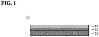
- the substrate 20 is, for example, a flat niobium metal plate material for depositing the conductive diamond film 40 and for supporting the conductive diamond film 40.
- the size and thickness of the main surface of the substrate 20 are not particularly limited, but for example, the main surface has a rectangular shape with one side measuring 20 mm to 500 mm, and a thickness measuring 0.5 mm to 5 mm.
- the niobium carbide layer 30 is formed, for example, on at least one main surface of the substrate 20, and is a layer formed by a reaction between a part of the niobium metal of the substrate 20 and a carbon source 22 described below.
- the niobium carbide layer 30 functions, for example, as an intermediate layer to increase a nucleation density of diamond crystals.
- the thickness of the niobium carbide layer 30 is set to 0.5 ⁇ m or more, the nucleation density of the diamond crystals for forming the conductive diamond film 40 can be sufficiently increased.
- the thickness of the niobium carbide layer 30 exceeds 5 ⁇ m, an internal stress increases, and there is a possibility that the diamond film-deposited substrate 10 will be warped.
- the internal stress can be reduced, and warping of the diamond film-deposited substrate 10 can be reduced.
- the conductive diamond film 40 is, for example, a polycrystalline film having electrical conductivity that is formed on the niobium carbide layer 30.
- the conductive diamond film 40 may be either a polycrystalline diamond film or a diamond-like carbon (DLC) film.
- the conductive diamond film 40 preferably contains, for example, boron at a concentration of 1 ⁇ 10 19 cm -3 or more and 1 ⁇ 10 22 cm -3 or less.
- the thickness of the conductive diamond film 40 is, for example, 0.5 ⁇ m or more and 10 ⁇ m or less, and from the viewpoint of maintaining a balance between durability and cost, it is preferably 1 ⁇ m or more and 5 ⁇ m or less. This embodiment shows a case in which the conductive diamond film 40 has a single layer structure.
- no pinholes reaching the substrate 20 or the niobium carbide layer 30 are present within a field of view of 1 mm ⁇ 1 mm, and it is particularly preferable that no pinholes are present over an entire surface of the conductive diamond film 40.
- the cross section (longitudinal or transverse section) of the conductive diamond film 40 is observed using, for example, a scanning electron microscope (for example, 5000 times magnification), it is preferable that no pinholes reaching the substrate 20 or the niobium carbide layer 30 are present within a 20 ⁇ m ⁇ 20 ⁇ m field of view. That is, in the conductive diamond film 40, not only pinholes observable from the surface but also internal pinholes are reduced. Thereby, the durability of the diamond electrode can be further improved.
- no pinholes reaching the substrate 20 or the niobium carbide layer 30 are present within a field of view of 1 mm ⁇ 1 mm in the cross section (longitudinal or transverse section) of the conductive diamond film 40, and it is particularly preferable that no pinholes are present over an entire cross section of the conductive diamond film 40.
- a continuous niobium carbide layer 30 having a thickness of 0.5 ⁇ m or more is formed over a width (length in a direction parallel to the main surface of the substrate 20) of 20 ⁇ m or more.
- the main component of the niobium carbide layer 30 is preferably niobium carbide, for example, having a chemical formula NbC. Thereby, the nucleation density of the diamond crystals for forming the conductive diamond film 40 can be increased.
- the main component of the niobium carbide layer 30 can be confirmed by, for example, X-ray diffraction (XRD).
- the crystallite size of the niobium carbide contained in the niobium carbide layer 30 is preferably, for example, 1 nm or more and 60 nm or less. When the crystallite size is outside the above range, it may be difficult to form the continuous niobium carbide layer 30 having a thickness of 0.5 ⁇ m or more. In contrast, with the crystallite size within the above range, the continuous niobium carbide layer 30 having a thickness of 0.5 ⁇ m or more is easily formed, and as a result, the occurrence of pinholes is easily suppressed. In this specification, each crystallite size can be measured, for example, by the Scherrer method of XRD.
- the crystallite size of the niobium metal contained in the substrate 20 is preferably, for example, 30 nm or more and 90 nm or less.
- the crystallite size of the niobium metal is less than 30 nm, it may be difficult to form the continuous niobium carbide layer 30. Meanwhile, by setting the crystallite size of the niobium metal to 30 nm or more, the continuous niobium carbide layer 30 is easily formed.
- the crystallite size of the niobium metal exceeds 90 nm, the difference in crystallite size with respect to the niobium carbide contained in the niobium carbide layer 30 becomes large, and cracks, etc., may occur. Meanwhile, by setting the crystallite size of the niobium metal to 90 nm or less, the crystallite size is distributed so as to gradually decrease from the substrate 20 to the niobium carbide layer 30, so the occurrence of cracks, etc., can be suppressed.
- the diamond film-deposited substrate 10 is measured by XRD (from the conductive diamond film 40 side), peaks such as Nb (110), Nb (200), and Nb (211) are observed, with the Nb (110) peak being the strongest. Therefore, in this specification, unless otherwise specified, the crystallite size of the niobium metal was calculated from the peak of Nb (110).
- the diamond film-deposited substrate 10 of this embodiment can be used to manufacture a diamond electrode for an electrochemical reaction (e.g., for ozone generation). Therefore, the present invention is also applicable as a method for manufacturing a diamond electrode.
- FIG. 2 is a flow chart showing an example of the method for manufacturing a diamond film-deposited substrate 10 of this embodiment.
- the method for manufacturing a diamond film-deposited substrate 10 of this embodiment includes, for example, an unevenness forming step S101, a processing damage layer forming step S102, a carbon source embedding step S103, a seeding step S104, a niobium carbide layer forming step S105, and a diamond film depositing step S106.
- This embodiment shows a case in which the diamond film-deposited substrate 10 is manufactured from the substrate 20 comprising niobium metal.
- the unevenness forming step S101 is, for example, a step of performing processing to form unevenness on at least one main surface of the substrate 20. Thereby, peeling caused by a difference in thermal expansion coefficient between the substrate 20 and the conductive diamond film 40, can be suppressed. That is, a peel strength of the diamond film-deposited substrate 10 can be further improved.
- the processing for forming the unevenness can be performed by a known method such as grinding, blasting, wet etching, and dry etching.
- the unevenness forming step S101 is preferably performed, for example, before the processing damage layer forming step S102.
- the processing for forming unevenness is performed to the surface on which the processing damage layer 21 is formed, there is a possibility that the processing damage layer 21 will be removed.
- the unevenness forming step S101 before the processing damage layer forming step S102, work-hardening occurs in the substrate 20, and therefore microcracks are likely to be formed in the processing damage layer forming step S102.
- further machining such as punching or grooving may be performed.
- the unevenness forming step S101 may be omitted.
- the niobium carbide layer 30 that continuously covers the main surface of the substrate 20 can be formed in the niobium carbide layer forming step S105. That is, the occurrence of pinholes on the conductive diamond film 40 can be suppressed.
- FIG. 3(a) is a schematic view illustrating the processing damage layer forming step S102.
- the processing damage layer forming step S102 is a step of forming a processing damage layer 21 having a large number of microcracks by introducing processing damage onto at least one main surfaces of the substrate 20 (the surface on which unevenness is formed at least in the unevenness forming step S101).
- heating to over 2300 degrees is usually required, but by forming the processing damage layer 21, the diffusion of carbon atoms into the niobium metal is promoted even at a low temperature (for example, about 800 degrees), and the niobium carbide layer 30 becomes easier to be formed.
- the method for introducing processing damage is not particularly limited as long as it is a method capable of forming microcracks.
- processing damage can be introduced by grinding, imprinting, blasting, pressing, etc., to form the processing damage layer 21 having microcracks.
- the microcracks include not only cracks having a length of 0.1 ⁇ m or more and 2 ⁇ m or less and a width of 5 nm or more and 200 nm or less (hereinafter, this will also be referred to as microcracks with voids), but also grain boundaries where crystal defects are gathered and arranged at a high density (hereinafter, this will also be referred to as microcracks without voids).
- the microcracks as used herein do not necessarily involve voids. Microcracks can be confirmed, for example, by observing the main surface of the substrate 20 with a scanning electron microscope. Further, in the processing damage layer forming step S102, for example, it is preferable to form microcracks having a depth of 0.5 ⁇ m or more and 5 ⁇ m or less at a density of 10 8 /cm 2 or more and 10 9 /cm 2 or less. Thereby, the carbon source 22 can be more easily embedded inside the microcracks in the carbon source embedding step S103 described later.
- the processing damage layer forming step S102 for example, it is preferable to form the processing damage layer 21 with a thickness of 0.5 ⁇ m or more and 5 ⁇ m or less (more preferably, 0.8 ⁇ m or more and 2.5 ⁇ m or less).
- the niobium carbide layer forming step S105 described later at least a part of the processing damage layer 21 becomes the niobium carbide layer 30, so by setting the thickness of the processing damage layer 21 within the above range, it becomes easier to form the niobium carbide layer 30 with an appropriate thickness.
- the processing damage layer 21 may be formed as a region in which the crystallite size is 10% or more smaller than the crystallite size of the niobium metal before the processing damage layer 21 is formed.
- the crystallite size of the niobium metal in the processing damage layer 21 is 1 nm or more and 25 nm or less.
- the carbon source 22 is unlikely to diffuse into the processing damage layer 21, and it may be difficult to form a continuous niobium carbide layer 30.
- the surface area of the niobium metal becomes sufficiently large, making it easier to form the continuous niobium carbide layer 30.
- the crystallite size of the niobium metal in the processing damage layer 21 is preferably 1 nm or more.
- FIG. 3(b) is a schematic view illustrating the carbon source embedding step S103.
- the carbon source embedding step S103 is a step of embedding a carbon source 22 comprising a solid carbon or carbon compound inside the processing damage layer 21 (for example, inside microcracks with voids). Since the processing damage layer 21 has a large number of microcracks, the carbon source 22 can be easily embedded therein. Specifically, for example, the surface of the substrate 20 is sprinkled with the carbon source 22, and the surface is rubbed against another substrate 20 of the same size, whereby the carbon source 22 is embedded while being crushed until it is approximately the same size as the microcracks (for example, average particle size of 200 nm or less).
- the carbon source 22 is a solid, carbon atoms can be introduced into the processing damage layer 21 at a high concentration compared to a hydrocarbon gas, etc. This makes it easier for the carbon atoms to diffuse into the niobium metal of the processing damage layer 21, making it easier to form the continuous niobium carbide layer 30.
- the carbon source 22 for example, graphite, boron carbide, diamond powder, etc.
- diamond powder in order to enhance the reactivity with niobium metal, it is preferable to use diamond powder with at least its outer circumference covered with an amorphous layer (sp 2 carbon). From the viewpoint of enhancing the reactivity with niobium metal and reducing a cost, it is preferable to use graphite as the carbon source 22.
- An average particle size of the carbon source 22 is preferably 200 nm or less. Thereby, it becomes easier to embed the carbon source 22 inside the processing damage layer 21. Further, the surface area of the carbon source 22 is increased, and the reactivity with niobium metal can be improved.
- a lower limit of the average particle size of the carbon source 22 is not particularly limited, but is, for example, 5 nm or more.
- the carbon source embedding step S103 when graphite (average particle size: 5 to 200 nm) is embedded in the processing damage layer 21 as the carbon source 22, for example, it is preferable to embed the carbon source 22 of 0.1 ⁇ g/cm 2 or more and 10 ⁇ g/cm 2 or less.
- the amount of the embedded carbon source 22 is less than 0.1 ⁇ g/cm 2 , the carbonization of the niobium metal will be insufficient, and it may be difficult to form the continuous niobium carbide layer 30.
- the amount of the embedded carbon source 22 is sufficiently carbonized, and the continuous niobium carbide layer 30 is easily formed.
- the amount of the embedded carbon source 22 exceeds 10 ⁇ g/cm 2 , a large amount of carbon source 22 remains after the formation of the niobium carbide layer 30, which may adversely affect the deposition of the conductive diamond film 40.
- the amount of the embedded carbon source 22 is set to 10 ⁇ g/cm 2 or less, the amount of a residual carbon source 22 can be reduced.
- the seeding step S104 is, for example, a step of seeding diamond particles on the main surface of the substrate 20 (the main surface on which the processing damage layer 21 is formed, that is, the surface of the processing damage layer 21).
- the method for seeding with diamond particles can be a known method such as blasting or immersion.
- the seeding step S104 is preferably performed, for example, before the niobium carbide layer 30 is formed (that is, before the niobium carbide layer forming step S105). This allows the niobium carbide layer forming step S105 and the diamond film depositing step S106, which will be described later, to be performed continuously within the same apparatus. Further, in this case, the seeding step S104 may be performed simultaneously with the carbon source embedding step S103 described above. That is, the carbon source 22 used in the carbon source embedding step S103 and the diamond particles used in the seeding step S104 can be the same diamond particles. As described above, the carbon source 22 preferably contains sp 2 carbon.
- diamond particles e.g., nanodiamond particles obtained by detonation method
- a diamond structure sp 3 structure
- an amorphous layer sp 2 carbon
- the seeding step S104 may be omitted. Even when the seeding step S104 is omitted, by performing the above-described processing damage layer forming step S102 and carbon source embedding step S103, the niobium carbide layer 30 that continuously covers the main surface of the substrate 20 can be formed in the niobium carbide layer forming step S105. That is, the occurrence of pinholes on the conductive diamond film 40 can be suppressed.
- the niobium carbide layer forming step S105 is a step of forming a niobium carbide layer 30 that continuously covers the main surface of the substrate 20 by applying heat treatment to the processing damage layer 21 and causing the niobium metal to react with the carbon source 22. Thereby, the occurrence of pinholes on the surface of the conductive diamond film 40, can be suppressed.
- a structure is reconstructed at the same time as the niobium carbide layer 30 is formed, and most of the microcracks formed in the processing damage layer forming step S102 disappear. Further, in the processing damage layer 21 that remains without reacting with the carbon source 22, the processing damage is recovered to a certain extent and the strength is increased, because defects disappear and decrease due to solid-phase diffusion at grain boundaries.
- the niobium carbide layer forming step S105 it is preferable to form the niobium carbide layer 30 having a thickness of, for example, 10% to 100% (more preferably, 30% to 100%) of the processing damage layer 21. In other words, it is preferable that a depth range from the surface to 10% or more of the thickness of the processing damage layer 21 is reacted with the carbon source 22 to form the niobium carbide layer 30.
- the thickness of the niobium carbide layer 30 is less than 10% of the thickness of the processing damage layer 21, the nucleation density of the diamond crystals will be insufficient, which may cause pinholes.
- niobium carbide layer forming step S105 for example, it is preferable to form the niobium carbide layer 30 containing niobium carbide of the chemical formula NbC as a main component. Thereby, the nucleation density of the diamond crystals for forming the conductive diamond film 40, can be increased.
- the diamond film depositing step S106 is, for example, a step of depositing a conductive diamond film 40 on the niobium carbide layer 30.
- the continuous niobium carbide layer 30 is formed in the above-described niobium carbide layer forming step S105, and therefore the occurrence of pinholes on the surface of the conductive diamond film 40 can be suppressed.
- the conductive diamond film 40 can be deposited using, for example, a hot filament CVD apparatus.
- the hot filament CVD apparatus is configured so as to be able to supply various gases, such as hydrogen gas, carbon-containing gas, and boron-containing gas, to a growth chamber.
- FIG. 4 is a schematic view illustrating the cross section of the diamond film-deposited substrate 10 of this modified example.
- the diamond film-deposited substrate 10 of this modified example has, for example, a substrate 20, a niobium carbide layer 30, and a conductive diamond film 40, and the niobium carbide layer 30 can be divided into an upper portion 31 and a lower portion 32.
- a method for manufacturing a diamond film-deposited substrate according to any one of the supplementary descriptions 8 to 15, wherein in the forming the niobium carbide layer, the niobium carbide layer is formed so that a crystal grain size of niobium carbide contained in the niobium carbide layer is 1 nm or more and 60 nm or less.
Landscapes
- Chemical & Material Sciences (AREA)
- Engineering & Computer Science (AREA)
- Materials Engineering (AREA)
- Organic Chemistry (AREA)
- Metallurgy (AREA)
- Chemical Kinetics & Catalysis (AREA)
- Mechanical Engineering (AREA)
- Inorganic Chemistry (AREA)
- General Chemical & Material Sciences (AREA)
- Crystallography & Structural Chemistry (AREA)
- Ceramic Engineering (AREA)
- Crystals, And After-Treatments Of Crystals (AREA)
- Chemical Vapour Deposition (AREA)
- Laminated Bodies (AREA)
- Electrodes For Compound Or Non-Metal Manufacture (AREA)
- Electrolytic Production Of Non-Metals, Compounds, Apparatuses Therefor (AREA)
- Other Surface Treatments For Metallic Materials (AREA)
Applications Claiming Priority (2)
| Application Number | Priority Date | Filing Date | Title |
|---|---|---|---|
| JP2022072370 | 2022-04-26 | ||
| PCT/JP2023/008214 WO2023210167A1 (ja) | 2022-04-26 | 2023-03-06 | ダイヤモンド膜堆積基板、およびダイヤモンド膜堆積基板の製造方法 |
Publications (1)
| Publication Number | Publication Date |
|---|---|
| EP4516973A1 true EP4516973A1 (en) | 2025-03-05 |
Family
ID=88518538
Family Applications (1)
| Application Number | Title | Priority Date | Filing Date |
|---|---|---|---|
| EP23795915.0A Pending EP4516973A1 (en) | 2022-04-26 | 2023-03-06 | Substrate with deposited diamond film and method for producing substrate with deposited diamond film |
Country Status (4)
| Country | Link |
|---|---|
| US (1) | US20250277306A1 (https=) |
| EP (1) | EP4516973A1 (https=) |
| JP (2) | JP7421018B1 (https=) |
| WO (1) | WO2023210167A1 (https=) |
Family Cites Families (6)
| Publication number | Priority date | Publication date | Assignee | Title |
|---|---|---|---|---|
| JP2938552B2 (ja) * | 1990-10-17 | 1999-08-23 | 富士通株式会社 | コーティング膜の製造方法およびコーティング膜の製造装置 |
| JP2002265296A (ja) * | 2001-03-09 | 2002-09-18 | Kobe Steel Ltd | ダイヤモンド薄膜及びその製造方法 |
| JP4581998B2 (ja) * | 2003-05-26 | 2010-11-17 | 住友電気工業株式会社 | ダイヤモンド被覆電極及びその製造方法 |
| JP4456378B2 (ja) | 2004-02-24 | 2010-04-28 | ペルメレック電極株式会社 | 導電性ダイヤモンド電極の製造方法 |
| JP4851376B2 (ja) * | 2007-03-23 | 2012-01-11 | 東海旅客鉄道株式会社 | ダイヤモンド膜の合成に用いる導電性基体の前処理方法及びダイヤモンド膜の製造方法 |
| KR101480023B1 (ko) * | 2014-05-29 | 2015-01-07 | 주식회사 아벡테크 | 다이아몬드 전극 및 그 제조 방법 |
-
2023
- 2023-03-06 US US18/859,148 patent/US20250277306A1/en active Pending
- 2023-03-06 JP JP2023561231A patent/JP7421018B1/ja active Active
- 2023-03-06 EP EP23795915.0A patent/EP4516973A1/en active Pending
- 2023-03-06 WO PCT/JP2023/008214 patent/WO2023210167A1/ja not_active Ceased
-
2024
- 2024-01-11 JP JP2024002365A patent/JP2024036357A/ja active Pending
Also Published As
| Publication number | Publication date |
|---|---|
| JP2024036357A (ja) | 2024-03-15 |
| JP7421018B1 (ja) | 2024-01-23 |
| JPWO2023210167A1 (https=) | 2023-11-02 |
| US20250277306A1 (en) | 2025-09-04 |
| WO2023210167A1 (ja) | 2023-11-02 |
Similar Documents
| Publication | Publication Date | Title |
|---|---|---|
| Dong et al. | Study on conductivity and corrosion resistance of N-doped and Cr/N co-doped DLC films on bipolar plates for PEMFC | |
| EP2520691B1 (en) | Tantalum carbide-coated carbon material and manufacturing method for same | |
| CN102388494B (zh) | 基于钛的材料、制造基于钛的材料的方法以及燃料电池分隔器 | |
| JP4581998B2 (ja) | ダイヤモンド被覆電極及びその製造方法 | |
| JP5275567B2 (ja) | 炭化タンタル被覆炭素材料およびその製造方法 | |
| Soin et al. | Microstructural and electrochemical properties of vertically aligned few layered graphene (FLG) nanoflakes and their application in methanol oxidation | |
| EP2333136A1 (en) | Diamond electrode and method for manufacturing diamond electrode | |
| JP5759534B2 (ja) | 被覆黒鉛物品、ならびに反応性イオンエッチングによる黒鉛物品の製造および再生 | |
| EP2210968A1 (en) | Carbonaceous substrate and electrode for electrolytic production of fluorine | |
| KR101209791B1 (ko) | 연료전지용 금속분리판 및 이의 표면처리방법 | |
| Liu et al. | Direct growth of few-layered graphene on boron doped diamond surface with varying boron doping concentration | |
| KR101968604B1 (ko) | 그래핀이 코팅된 스테인리스 스틸(sus) 지지체 및 이의 제조 방법 | |
| CN108486546B (zh) | 一种bdd膜电极材料及其制备方法 | |
| EP4516973A1 (en) | Substrate with deposited diamond film and method for producing substrate with deposited diamond film | |
| CN113072063B (zh) | 基于氢储运设备内表面的阻氢涂层及制备方法 | |
| JP7348422B1 (ja) | ダイヤモンド電極、およびダイヤモンド電極の製造方法 | |
| CN112981365A (zh) | 一种网笼多层结构硼掺杂金刚石电极的制备方法 | |
| Ray et al. | Deposition and characterization of diamond-like carbon thin films by electro-deposition technique using organic liquid | |
| EP1967497A2 (en) | Granular diamond and diamond electrode using the same | |
| JP3929140B2 (ja) | 耐蝕性部材およびその製造方法 | |
| JP7322315B1 (ja) | ダイヤモンド電極 | |
| Ahmed et al. | Advanced Molybdenum Carbide films for Graphite Bipolar Plates: Enhancing Durability and Electrochemical Performance for PEM Fuel Cells | |
| Argoitia et al. | Electrochemical studies of boron-doped diamond electrodes | |
| Zhang et al. | Influence of geometry factors of in situ dc glow discharge on the diamond nucleation in a hot-filament chemical vapor deposition system | |
| EP4394091A1 (en) | Semiconductor heat treatment member |
Legal Events
| Date | Code | Title | Description |
|---|---|---|---|
| STAA | Information on the status of an ep patent application or granted ep patent |
Free format text: STATUS: THE INTERNATIONAL PUBLICATION HAS BEEN MADE |
|
| PUAI | Public reference made under article 153(3) epc to a published international application that has entered the european phase |
Free format text: ORIGINAL CODE: 0009012 |
|
| STAA | Information on the status of an ep patent application or granted ep patent |
Free format text: STATUS: REQUEST FOR EXAMINATION WAS MADE |
|
| 17P | Request for examination filed |
Effective date: 20241010 |
|
| AK | Designated contracting states |
Kind code of ref document: A1 Designated state(s): AL AT BE BG CH CY CZ DE DK EE ES FI FR GB GR HR HU IE IS IT LI LT LU LV MC ME MK MT NL NO PL PT RO RS SE SI SK SM TR |
|
| DAV | Request for validation of the european patent (deleted) | ||
| DAX | Request for extension of the european patent (deleted) |