EP4506707A1 - Magnetic field detection device and magnetic field detection device array - Google Patents
Magnetic field detection device and magnetic field detection device array Download PDFInfo
- Publication number
- EP4506707A1 EP4506707A1 EP24193278.9A EP24193278A EP4506707A1 EP 4506707 A1 EP4506707 A1 EP 4506707A1 EP 24193278 A EP24193278 A EP 24193278A EP 4506707 A1 EP4506707 A1 EP 4506707A1
- Authority
- EP
- European Patent Office
- Prior art keywords
- magnetic field
- magnetic
- field detection
- detection device
- cutout
- Prior art date
- Legal status (The legal status is an assumption and is not a legal conclusion. Google has not performed a legal analysis and makes no representation as to the accuracy of the status listed.)
- Pending
Links
Images




Classifications
-
- G—PHYSICS
- G01—MEASURING; TESTING
- G01R—MEASURING ELECTRIC VARIABLES; MEASURING MAGNETIC VARIABLES
- G01R33/00—Arrangements or instruments for measuring magnetic variables
- G01R33/02—Measuring direction or magnitude of magnetic fields or magnetic flux
- G01R33/0206—Three-component magnetometers
-
- G—PHYSICS
- G01—MEASURING; TESTING
- G01R—MEASURING ELECTRIC VARIABLES; MEASURING MAGNETIC VARIABLES
- G01R33/00—Arrangements or instruments for measuring magnetic variables
- G01R33/02—Measuring direction or magnitude of magnetic fields or magnetic flux
-
- G—PHYSICS
- G01—MEASURING; TESTING
- G01R—MEASURING ELECTRIC VARIABLES; MEASURING MAGNETIC VARIABLES
- G01R33/00—Arrangements or instruments for measuring magnetic variables
- G01R33/0047—Housings or packaging of magnetic sensors ; Holders
-
- G—PHYSICS
- G01—MEASURING; TESTING
- G01R—MEASURING ELECTRIC VARIABLES; MEASURING MAGNETIC VARIABLES
- G01R33/00—Arrangements or instruments for measuring magnetic variables
- G01R33/0094—Sensor arrays
Definitions
- the present disclosure relates to a magnetic field detection device and, more particularly, to a magnetic field detection device capable of detecting a magnetic field in three-axis directions.
- the present disclosure also relates to a magnetic field detection device array having a plurality of such magnetic field detection devices.
- Japanese Unexamined Utility Model Application Publication No. 58-047181 discloses a magnetic field detection device capable of detecting a magnetic field in three-axis directions.
- the magnetic field detection device disclosed in Japanese Unexamined Utility Model Application Publication No. 58-047181 is disadvantageously likely to have magnetic interference between a plurality of magnetic sensors.
- the present disclosure describes a technology for reducing magnetic interference between magnetic sensors in a magnetic field detection device capable of detecting a magnetic field in three-axis directions.
- a magnetic field detection device includes a support having first, second, and third cutouts and first, second, and third magnetic sensors respectively accommodated in the first, second, and third cutouts.
- the support has first and second surfaces extending in a first direction and a second direction perpendicular to the first direction and different in position in a third direction perpendicular to both the first and second directions, third and fourth surfaces extending in the first and third directions and different in position in the second direction, and fifth and sixth surfaces extending in the second and third directions and different in position in the first direction.
- the first cutout is formed in at least one of the first and fourth surfaces
- the second cutout is formed in at least one of the second and fifth surfaces
- the third cutout is formed in at least one of the third and sixth surfaces.
- the first magnetic sensor has its magnetic sensing direction along the first direction
- the second magnetic sensor has its magnetic sensing direction along the second direction
- the third magnetic sensor has its magnetic sensing direction along the third direction.
- a magnetic field detection device capable of detecting a magnetic field in three-axis directions, offering a technology for reducing magnetic interference between magnetic sensors.
- FIGS. 1A and 1B are schematic perspective views as viewed in different directions, which illustrate the outer appearance of a magnetic field detection device 100 according to an embodiment of the technology according to the present disclosure.
- the magnetic field detection device 100 includes a support 10 made of a nonmagnetic material such as resin and three magnetic sensors S1 to S3 supported by the support 10.
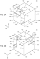
- FIGS. 2A and 2B are schematic perspective views as viewed from different directions, which illustrates the structure of the support 10.
- the support 10 has a structure obtained by partially forming cutouts 121 to 123 in a rectangular parallelepiped block.
- the cutouts 121 to 123 may be formed by machining the rectangular parallelepiped block, or may be formed simultaneously with the support 10 by using a die. According to the latter method, relative positional accuracy between the cutouts 121 to 123 is improved.
- the cutouts 121, 122, and 123 respectively accommodate the magnetic sensors S1, S2, and S3. More specifically, the support 10 has surfaces 11, 12 constituting the XY surface and positioned at mutually opposite sides in the Z-direction, surfaces 13, 14 constituting the XZ surface and positioned at mutually opposite sides in the Y-direction, and surfaces 15, 16 constituting the YZ surface and positioned at mutually opposite sides in the X-direction.
- the support 10 has a through hole 17 extending in the Z-direction from the surface 11 to the surface 12.
- FIGS. 2A and 2B virtual sides that should originally exist when the support 10 does not have the cutouts 121 to 123 are denoted by dashed lines. That is, when the cutouts 121 to 123 and through hole 17 are absent, the support 10 may have a rectangular parallelepiped shape or a cubic shape. In the example illustrated in FIGS. 2A and 2B , the support 10 has a rectangular parallelepiped shape in which the sizes in the X- and Y-directions are the same, and the size in the Z-direction is slightly smaller than the sizes in the X- and Y-directions.
- the surface 11 is perpendicular to surfaces 13 to 16.
- the end portion of the surface 11 at the positive Y-direction side and the end portion of the surface 14 at the positive Z-direction side constitute a side 101.
- the end portion of the surface 11 at the negative Y-direction side and the end portion of the surface 13 at the positive Z-direction side constitute a side 107.
- the end portion of the surface 11 at the positive X-direction side and the end portion of the surface 16 at the positive Z-direction side constitute a side 104.
- the end portion of the surface 11 at the negative X-direction side and the end portion of the surface 15 at the positive Z-direction side constitute a side 112.
- the sides 101 and 107 extend in the X-direction, and the sides 104 and 112 extend in the Y-direction.
- the surface 12 is perpendicular to surfaces 13 to 16.
- the end portion of the surface 12 at the positive Y-direction side and the end portion of the surface 14 at the negative Z-direction side constitute a side 105.
- the end portion of the surface 12 at the negative Y-direction side and the end portion of the surface 13 at the negative Z-direction side constitute a side 106.
- the end portion of the surface 12 at the positive X-direction side and the end portion of the surface 16 at the negative Z-direction side constitute a side 108.
- the end portion of the surface 12 at the negative X-direction side and the end portion of the surface 15 at the negative Z-direction side constitute a side 102.
- the surfaces 13, 14 are perpendicular to surfaces 15, 16.
- the end portion of the surface 13 at the positive X-direction side and the end portion of the surface 16 at the negative Y-direction side constitute a side 103.
- the end portion of the surface 13 at the negative X-direction side and the end portion of the surface 15 at the negative Y-direction side constitute a side 111.
- the end portion of the surface 14 at the positive X-direction side and the end portion of the surface 16 at the positive Y-direction side constitute a side 110.
- the end portion of the surface 14 at the negative X-direction side and the end portion of the surface 15 at the positive Y-direction side constitute a side 109.
- the sides 103 and 109 to 111 extend in the Z-direction.
- the support 10 has eight vertices 131 to 138. Among them, three vertices 131, 132, and 133 have been removed respectively by the cutouts 121, 122, and 123 and are thus virtual vertices that should originally exist when the support 10 has a rectangular parallelepiped shape (or a cubic shape).
- the vertex 131 is a virtual vertex at which extension lines of the sides 101, 104, and 110 cross one another. In other words, the vertex 131 is constituted by the virtual end points of the surfaces 11, 14, and 16.
- the vertex 132 is a virtual vertex at which extension lines of the sides 102, 105, and 109 cross one another. In other words, the vertex 132 is constituted by the virtual end points of the surfaces 12, 14, and 15.
- the vertex 133 is a virtual vertex at which extension lines of the sides 103, 106, and 108 cross one another. In other words, the vertex 133 is constituted by the virtual end points of the surfaces 12, 13, and 16.
- no cutout is formed at the vertices 134 to 138. That is, the vertices 134 to 138 are actually existing vertices.
- the vertex 134 is constituted by the terminal portions of the sides 101, 109, and 112.
- the vertex 135 is constituted by the terminal portions of the sides 107, 111, and 112.
- the vertex 136 is constituted by the terminal portions of the sides 103, 104, and 107.
- the vertex 137 is constituted by the terminal portions of the sides 105, 108, and 110.
- the vertex 138 is constituted by the terminal portions of the sides 102, 106, and 111.
- the cutout 121 extends in the X-direction along the side 101 so as to cut the vertex 131.
- the cutout 121 has an inner wall 141 constituting the XY surface, an inner wall 142 constituting the XZ surface, and an inner wall 143 constituting the YZ surface.
- the positive Z-direction side of the inner wall 141 is opened except for a part thereof covered with a protrusion part 144 constituting a part of the surface 11.
- the positive Y-direction side of the inner wall 142 is opened except for a part thereof covered with a protrusion part 145 constituting a part of the surface 14.
- the positive X-direction side of the inner wall 143 is completely opened.
- the X-direction size of the cutout 121 is designed substantially the same as or slightly larger than the X-direction size of the magnetic sensor S1.
- the Z-direction distance between the inner wall 141 and an inner wall 144a of the protrusion part 144 is designed substantially the same as or slightly larger than the Z-direction size of the magnetic sensor S1.
- the Y-direction distance between the inner wall 142 and an inner wall 145a of the protrusion part 145 is designed substantially the same as or slightly larger than the Y-direction size of the magnetic sensor S1.
- the magnetic sensor S1 when the magnetic sensor S1 is inserted into the cutout 121 in the X-direction, the magnetic sensor S1 is positioned in the Z-direction by the inner wall 141 and the inner wall 144a of the protrusion part 144 and in the Y-direction by the inner wall 142 and the inner wall 145a of the protrusion part 145.
- a stopper 201 is screwed to the surface 16 so as to cover a part of the cutout 121 in the X-direction, as illustrated in FIG. 1B. This prevents the magnetic sensor S1 from coming off from the cutout 121.
- the cutout 122 extends in the Y-direction along the side 102 so as to cut the vertex 132.
- the cutout 122 has an inner wall 151 constituting the XY surface, an inner wall 152 constituting the YZ surface, and an inner wall 153 constituting the XZ surface.
- the negative Z-direction side of the inner wall 151 is opened except for a part thereof covered with a protrusion part 154 constituting a part of the surface 12.
- the negative X-direction side of the inner wall 152 is opened except for a part thereof covered with a protrusion part 155 constituting a part of the surface 15.
- the positive Y-direction side of the inner wall 153 is completely opened.
- the Y-direction size of the cutout 122 is designed substantially the same as or slightly larger than the Y-direction size of the magnetic sensor S2.
- the Z-direction distance between the inner wall 151 and an inner wall 154a of the protrusion part 154 is designed substantially the same as or slightly larger than the Z-direction size of the magnetic sensor S2.
- the X-direction distance between the inner wall 152 and an inner wall 155a of the protrusion part 155 is designed substantially the same as or slightly larger than the X-direction size of the magnetic sensor S2.
- the magnetic sensor S2 when the magnetic sensor S2 is inserted into the cutout 122 in the Y-direction, the magnetic sensor S2 is positioned in the Z-direction by the inner wall 151 and the inner wall 154a of the protrusion part 154 and in the X-direction by the inner wall 152 and the inner wall 155a of the protrusion part 155.
- a stopper 202 is screwed to the surface 14 so as to cover a part of the cutout 122 in the Y-direction, as illustrated in FIG. 1B. This prevents the magnetic sensor S2 from coming off the cutout 122.
- the cutout 123 extends in the Z-direction along the side 103 so as to cut the vertex 133.
- the cutout 123 has an inner wall 161 constituting the XZ surface, an inner wall 162 constituting the YZ surface, and an inner wall 163 constituting the XY surface.
- the negative Y-direction side of the inner wall 161 is opened except for a part thereof covered with a protrusion part 164 constituting a part of the surface 13.
- the positive X-direction side of the inner wall 162 is opened except for a part thereof covered with a protrusion part 165 constituting a part of the surface 16.
- the negative Z-direction side of the inner wall 163 is completely opened.
- the Z-direction size of the cutout 123 is designed substantially the same as or slightly larger than the Z-direction size of the magnetic sensor S3.
- the Y-direction distance between the inner wall 161 and an inner wall 164a of the protrusion part 164 is designed substantially the same as or slightly larger than the Y-direction size of the magnetic sensor S3.
- the X-direction distance between the inner wall 162 and an inner wall 165a of the protrusion part 165 is designed substantially the same as or slightly larger than the X-direction size of the magnetic sensor S3.
- the magnetic sensor S3 when the magnetic sensor S3 is inserted into the cutout 123 in the Z-direction, the magnetic sensor S3 is positioned in the Y-direction by the inner wall 161 and the inner wall 164a of the protrusion part 164 and in the X-direction by the inner wall 162 and the inner wall 165a of the protrusion part 165.
- a stopper 203 is screwed to the surface 12 so as to cover a part of the cutout 123 in the Z-direction, as illustrated in FIG. 1B. This prevents the magnetic sensor S3 from coming off the cutout 123.
- FIG. 3 is a schematic transparent perspective view of the structure of the magnetic sensor S1, which illustrates a state where a resin case constituting a housing of the magnetic sensor S1 is removed.
- the magnetic sensor S1 has a substrate 211 elongated in the X-direction and a magnetosensitive element 212 mounted in the vicinity of the leading end of the substrate 211 in the positive X-direction.
- the magnetic sensing direction of the magnetosensitive element 212 is the X-direction.
- an end face 210 in the positive X-direction of the resin case constituting a housing of the magnetic sensor S1 constitutes a sensor head of the magnetic sensor S1, and an X-direction magnetic field in a space around the end face 210 is detected by the magnetic sensor S1.
- the magnetosensitive element 212 is connected to a connector 214 by way of cables 213 fixed to the substrate 211.
- the magnetic sensors S2 and S3 have the same configuration as the magnetic sensor S1.
- the magnetic sensor S2 has, in the housing thereof, a magnetosensitive element 212 whose magnetic sensing direction is the Y-direction, and an end face in the positive Y-direction of the resin case constituting the sensor housing constitutes a sensor head.
- the magnetic sensor S3 has, in the housing thereof, a magnetosensitive element 212 whose magnetic sensing direction is the Z-direction, and an end face in the negative Z-direction of the resin case constituting the sensor housing constitutes a sensor head. That is, the magnetic sensors S1 to S3 may have the same structure.
- the magnetic sensors S1, S2, and S3 having mutually different sensitivity axis directions are accommodated respectively in the cutouts 121, 122, and 123 formed in the support 10, thereby allowing a magnetic field to be detected in three-axis directions (X-, Y-, and Z-directions).
- the cutouts 121, 122, and 123 are respectively arranged along the sides 101, 102, and 103 that do not cross one another (do not have a common vertex), thereby making it possible to prevent physical interference between the magnetic sensors S1 to S3.
- an appropriate distance can be ensured between the sensor heads of the respective magnetic sensors S1, S2, and S3, making it possible to reduce also magnetic interference between the magnetic sensors S1 to S3.
- the magnetic sensors S1 and S2 do not overlap each other in the Z-direction, and the magnetic sensors S2 and S3 do not overlap each other in the X-direction, thereby preventing magnetic interference between the magnetic sensors S1 and S2 and magnetic interference between the magnetic sensors S2 and S3.
- the magnetic sensors S1 and S3 slightly overlap each other in the Y-direction in the present embodiment, the magnetic sensors S1 and S3 may be configured so as not to overlap each other in the Y-direction by designing the X-, Y-, and Z-direction sizes of the support 10 substantially the same.
- the cutouts 121, 122, and 123 have their inner walls for respectively positioning the magnetic sensors S1, S2, and S3, thereby allowing the magnetic sensors S1 to S3 to be positioned along the inner walls of the cutouts 121 to 123 with high accuracy. Further, the magnetic sensors S1 to S3 do not protrude from the surfaces 11 to 16 of the support 10, so that miniaturization can be achieved, and a plurality of the magnetic field detection devices 100 can be arranged in proximity to one another in an array.
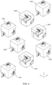
- FIG. 4 is a schematic perspective view of a magnetic field detection device array having a structure in which a plurality of the magnetic field detection devices 100 are arranged in an array.
- the magnetic field detection device array illustrated in FIG. 4 has a structure in which eight magnetic field detection devices 100A to 100H are arranged in an array.
- the magnetic field detection devices 100A to 100C are arranged in the X-direction
- the magnetic field detection devices 100D and 100E are arranged in the X-direction
- the magnetic field detection devices 100F to 100H are arranged in the X-direction.
- the positions of the magnetic field detection devices 100A to 100H in the Y-direction are the same.
- the magnetic field detection devices 100A and 100F are arranged in the Z-direction, the magnetic field detection devices 100B and 100G are arranged in the Z-direction, and the magnetic field detection devices 100C and 100H are arranged in the Z-direction. These magnetic field detection devices 100A to 100H can be fixed at desired positions within a measurement space by means of shafts inserted through the through holes 17 formed in the supports 10.
- the X-direction position of the magnetic field detection device 100D is intermediate between the X-direction position of the magnetic field detection devices 100A and 100F and the X-direction position of the magnetic field detection devices 100B and 100G.
- the Z-direction position of the magnetic field detection device 100D is intermediate between the Z-direction position of the magnetic field detection devices 100A to 100C and the Z-direction position of the magnetic field detection devices 100F to 100H.
- the X-direction position of the magnetic field detection device 100E is intermediate between the X-direction position of the magnetic field detection devices 100B and 100G and the X-direction position of the magnetic field detection devices 100C and 100H.
- the Z-direction position of the magnetic field detection device 100E is intermediate between the Z-direction position of the magnetic field detection devices 100A to 100C and the Z-direction position of the magnetic field detection devices 100F to 100H.
- the array arrangement of the plurality of magnetic field detection devices 100 can detect a magnetic field over a wider space range.
- the supports 10 of two magnetic field detection devices adjacent in the X-direction differ in orientation from each other by 180°.
- the support 10 of the magnetic field detection device 100B is fixed in a direction obtained by rotating the support 10 of the magnetic field detection device 100A about the Z-axis.
- the sensitivity axis of the magnetic sensor S1 included in the magnetic field detection device 100A and the sensitivity axis of the magnetic sensor S1 included in the magnetic field detection device 100B do not coincide with each other but are shifted from each other in the Y-direction, thus making it possible to more efficiently detect a magnetic field within a measurement space.
- the direction of each arrow denotes the magnetic sensing direction, and the position thereof denotes a detection position (sensor head position).
- the plurality of magnetic field detection devices are spaced apart from one another in the example illustrated in FIG. 4 , they may be arranged such that the supports 10 of adjacent magnetic field detection devices contact one another.
- a spacer or the like may be interposed between adjacent magnetic field detection devices so as to fix the interval therebetween.
- FIGS. 6A to 6C are schematic views for explaining a method of taking out signals output from the three magnetic sensors S1 to S3 included in the magnetic field detection device 100.
- FIGS. 6A, 6B, and 6C illustrate first, second, and third examples, respectively.
- cables 301, 302, and 303 connected respectively to the magnetic sensors S1, S2, and S3 are separately drawn from the magnetic field detection device 100.
- the cables 301, 302, and 303 may include not only signal cables for transmitting signals output from the magnetic sensors S1, S2, and S3 but also power cables for supplying operation power supply to the magnetic sensors S1 to S3 and ground cables.
- the configuration of the magnetic field detection device 100 is made simple.
- the magnetic field detection device 100 includes a circuit board 311, and the magnetic sensors S1 to S3 are connected to a cable 312 through the circuit board 311.
- the cable 312 may include not only a signal cable for transmitting signals output from the magnetic sensors S1 to S3 but also a power cable for supplying operation power supply to the magnetic sensors S1 to S3. According to the second example of FIG. 6B , the numbers of cables and connectors externally drawn from the magnetic field detection device 100 can be reduced.
- the magnetic field detection device 100 includes an AD converter 321 and a controller 322, and the controller 322 is connected with a cable 323.
- the AD converter 321 AD converts an analog signal output from the magnetic sensors S1 to S3 to generate a digital signal.
- the digital signal output from the AD converter 321 is supplied to the controller 322 to be subjected to signal processing therein.
- the controller 322 is connected with the cable 323.
- the cable 323 may include not only a signal cable for transmitting signals output from the magnetic sensors S1 to S3 but also a power cable for supplying operation power supply to the magnetic sensors S1 to S3.
- a digital signal is output from the magnetic field detection device 100, thus facilitating handling of the magnetic field detection device 100.
- the cutouts 121, 122, and 123 of the support 10 are disposed so as to respectively cut the sides 101, 102, and 103 of the support 10 in the above embodiment, the cutouts 121, 122, and 123 need not respectively cut the sides 101, 102, and 103 themselves.
- the cutouts 121, 122, and 123 may be formed respectively along the sides 101, 102, and 103 without respectively cutting the sides 101, 102, and 103 themselves.
- the cutout 121 may be formed in one of the surfaces 11 and 14 along the side 101
- the cutout 122 may be formed in one of the surfaces 12 and 15 along the side 102
- the cutout 123 may be formed in one of the surfaces 13 and 16 along the side 103.
- the technology according to the present disclosure includes the following configuration examples, but not limited thereto.
- a magnetic field detection device includes a support having first, second, and third cutouts and first, second, and third magnetic sensors respectively accommodated in the first, second, and third cutouts.
- the support has first and second surfaces extending in a first direction and a second direction perpendicular to the first direction and different in position in a third direction perpendicular to both the first and second directions, third and fourth surfaces extending in the first and third directions and different in position in the second direction, and fifth and sixth surfaces extending in the second and third directions and different in position in the first direction.
- the first cutout is formed in at least one of the first and fourth surfaces
- the second cutout is formed in at least one of the second and fifth surfaces
- the third cutout is formed in at least one of the third and sixth surfaces.
- the first magnetic sensor has its magnetic sensing direction along the first direction
- the second magnetic sensor has its magnetic sensing direction along the second direction
- the third magnetic sensor has its magnetic sensing direction along the third direction.
- the first magnetic sensor may be accommodated in the first cutout without protruding from the first and fourth surfaces
- the second magnetic sensor may be accommodated in the second cutout without protruding from the second and fifth surfaces
- the third magnetic sensor may be accommodated in the third cutout without protruding from the third and sixth surfaces. This can reduce the entire size.
- the first cutout may extend along the first direction so as to cut a first side formed by the edges of the first and fourth surfaces
- the second cutout may extend along the second direction so as to cut a second side formed by the edges of the second and fifth surfaces
- the third cutout may extend along the third direction so as to cut a third side formed by the edges of the third and sixth surfaces.
- the first cutout may be formed so as to cut a first vertex constituted by end points of the first, fourth, and sixth surfaces
- the second cutout may be formed so as to cut a second vertex constituted by end points of the second, fourth, and fifth surfaces
- the third cutout may be formed so as to cut a third vertex constituted by end points of the second, third, and sixth surfaces.
- the first and second magnetic sensors need not overlap each other in the third direction. This can further reduce magnetic interference between the first and second magnetic sensors.
- the second and third magnetic sensors need not overlap each other in the first direction. This can further reduce magnetic interference between the second and third magnetic sensors.
- the first and third magnetic sensors need not overlap each other in the second direction. This can further reduce magnetic interference between the first and third magnetic sensors.
- a magnetic field detection device array has a plurality of the above-described magnetic field detection devices. This can detect a magnetic field within a measurement space over a wider range.
- two adjacent ones of the plurality of magnetic field detection devices may be arranged such that their supports differ in orientation from each other by 180°. This can detect a magnetic field within a measurement space more efficiently.
- the above magnetic field detection device may further include a first cable connected to the first magnetic sensor, a second cable connected to the second magnetic sensor, a third cable connected to the third magnetic sensor, and a fourth cable for externally and collectively drawing the first, second, and third cables. This can reduce the numbers of cables and connectors externally drawn from the magnetic field detection device.
- the above magnetic field detection device may further include an AD converter for AD converting analog signals output from the first, second, and third magnetic sensors and a controller for applying signal processing to the digital signal output from the AD converter. This allows a digital signal to be output from the magnetic field detection device.
Landscapes
- Physics & Mathematics (AREA)
- Condensed Matter Physics & Semiconductors (AREA)
- General Physics & Mathematics (AREA)
- Measuring Magnetic Variables (AREA)
Abstract
Disclosed herein is a magnetic field detection device that includes a support having first, second, and third cutouts; and first, second, and third magnetic sensors accommodated in the first, second, and third cutouts, respectively. The support has first and second surfaces extending in first and second directions, third and fourth surfaces extending in the first and third directions, and fifth and sixth surfaces extending in the second and third directions. The first cutout is formed in at least one of the first and fourth surfaces, the second cutout is formed in at least one of the second and fifth surfaces, and the third cutout is formed in at least one of the third and sixth surfaces. Magnetic sensing directions of the first, second, and third magnetic sensors are the first, second, and third directions, respectively.
Description
- The present disclosure relates to a magnetic field detection device and, more particularly, to a magnetic field detection device capable of detecting a magnetic field in three-axis directions. The present disclosure also relates to a magnetic field detection device array having a plurality of such magnetic field detection devices.
-
Japanese Unexamined Utility Model Application Publication No. 58-047181 - However, the magnetic field detection device disclosed in
Japanese Unexamined Utility Model Application Publication No. 58-047181 - The present disclosure describes a technology for reducing magnetic interference between magnetic sensors in a magnetic field detection device capable of detecting a magnetic field in three-axis directions.
- A magnetic field detection device according to an aspect of the present disclosure includes a support having first, second, and third cutouts and first, second, and third magnetic sensors respectively accommodated in the first, second, and third cutouts. The support has first and second surfaces extending in a first direction and a second direction perpendicular to the first direction and different in position in a third direction perpendicular to both the first and second directions, third and fourth surfaces extending in the first and third directions and different in position in the second direction, and fifth and sixth surfaces extending in the second and third directions and different in position in the first direction. The first cutout is formed in at least one of the first and fourth surfaces, the second cutout is formed in at least one of the second and fifth surfaces, and the third cutout is formed in at least one of the third and sixth surfaces. The first magnetic sensor has its magnetic sensing direction along the first direction, the second magnetic sensor has its magnetic sensing direction along the second direction, and the third magnetic sensor has its magnetic sensing direction along the third direction. With this configuration, a magnetic field can be detected in three-axis directions by the first to third magnetic sensors, and magnetic interference between the first to third magnetic sensors can be prevented.
- According to the present disclosure, there is provided a magnetic field detection device capable of detecting a magnetic field in three-axis directions, offering a technology for reducing magnetic interference between magnetic sensors.
- The above features and advantages of the present disclosure will be more apparent from the following description of certain preferred embodiments taken in conjunction with the accompanying drawings, in which:
-
FIGS. 1A and 1B are schematic perspective views as viewed in different directions, which illustrate the outer appearance of a magneticfield detection device 100 according to an embodiment of the technology according to the present disclosure; -
FIGS. 2A and 2B are schematic perspective views as viewed from different directions, which illustrates the structure of thesupport 10; -
FIG. 3 is a schematic transparent perspective view of the structure of the magnetic sensor S1, which illustrates a state where a resin case constituting a housing of the magnetic sensor S1 is removed; -
FIG. 4 is a schematic perspective view of a magnetic field detection device array having a structure in which a plurality of the magneticfield detection devices 100 are arranged in an array; -
FIG. 5 is a schematic diagram for explaining the orientations of the magneticfield detection device 100A and the magneticfield detection device 100B; and -
FIGS. 6A to 6C are schematic views for explaining a method of taking out signals output from the three magnetic sensors S1 to S3 included in the magneticfield detection device 100, whereFIGS. 6A, 6B, and 6C illustrate first, second, and third examples, respectively. - Some embodiments of the present disclosure will be explained below in detail with reference to the accompanying drawings.
-
FIGS. 1A and 1B are schematic perspective views as viewed in different directions, which illustrate the outer appearance of a magneticfield detection device 100 according to an embodiment of the technology according to the present disclosure. - As illustrated in
FIGS. 1A and 1B, the magneticfield detection device 100 according to the present embodiment includes asupport 10 made of a nonmagnetic material such as resin and three magnetic sensors S1 to S3 supported by thesupport 10. -
FIGS. 2A and 2B are schematic perspective views as viewed from different directions, which illustrates the structure of thesupport 10. - As illustrated in
FIGS. 2A and 2B , thesupport 10 has a structure obtained by partially formingcutouts 121 to 123 in a rectangular parallelepiped block. Thecutouts 121 to 123 may be formed by machining the rectangular parallelepiped block, or may be formed simultaneously with thesupport 10 by using a die. According to the latter method, relative positional accuracy between thecutouts 121 to 123 is improved. - The
cutouts support 10 hassurfaces surfaces surfaces support 10 has a throughhole 17 extending in the Z-direction from thesurface 11 to thesurface 12. - In
FIGS. 2A and 2B , virtual sides that should originally exist when thesupport 10 does not have thecutouts 121 to 123 are denoted by dashed lines. That is, when thecutouts 121 to 123 and throughhole 17 are absent, thesupport 10 may have a rectangular parallelepiped shape or a cubic shape. In the example illustrated inFIGS. 2A and 2B , thesupport 10 has a rectangular parallelepiped shape in which the sizes in the X- and Y-directions are the same, and the size in the Z-direction is slightly smaller than the sizes in the X- and Y-directions. - The
surface 11 is perpendicular tosurfaces 13 to 16. The end portion of thesurface 11 at the positive Y-direction side and the end portion of thesurface 14 at the positive Z-direction side constitute aside 101. The end portion of thesurface 11 at the negative Y-direction side and the end portion of thesurface 13 at the positive Z-direction side constitute aside 107. The end portion of thesurface 11 at the positive X-direction side and the end portion of thesurface 16 at the positive Z-direction side constitute aside 104. The end portion of thesurface 11 at the negative X-direction side and the end portion of thesurface 15 at the positive Z-direction side constitute aside 112. Thesides sides - The
surface 12 is perpendicular tosurfaces 13 to 16. The end portion of thesurface 12 at the positive Y-direction side and the end portion of thesurface 14 at the negative Z-direction side constitute aside 105. The end portion of thesurface 12 at the negative Y-direction side and the end portion of thesurface 13 at the negative Z-direction side constitute aside 106. The end portion of thesurface 12 at the positive X-direction side and the end portion of thesurface 16 at the negative Z-direction side constitute aside 108. The end portion of thesurface 12 at the negative X-direction side and the end portion of thesurface 15 at the negative Z-direction side constitute aside 102. Thesides sides 102 and 118 extend in the Y=direction. - The
surfaces surfaces surface 13 at the positive X-direction side and the end portion of thesurface 16 at the negative Y-direction side constitute aside 103. The end portion of thesurface 13 at the negative X-direction side and the end portion of thesurface 15 at the negative Y-direction side constitute aside 111. The end portion of thesurface 14 at the positive X-direction side and the end portion of thesurface 16 at the positive Y-direction side constitute aside 110. The end portion of thesurface 14 at the negative X-direction side and the end portion of thesurface 15 at the positive Y-direction side constitute aside 109. Thesides - The
support 10 has eightvertices 131 to 138. Among them, threevertices cutouts support 10 has a rectangular parallelepiped shape (or a cubic shape). Thevertex 131 is a virtual vertex at which extension lines of thesides vertex 131 is constituted by the virtual end points of thesurfaces vertex 132 is a virtual vertex at which extension lines of thesides vertex 132 is constituted by the virtual end points of thesurfaces vertex 133 is a virtual vertex at which extension lines of thesides vertex 133 is constituted by the virtual end points of thesurfaces - In the present embodiment, no cutout is formed at the
vertices 134 to 138. That is, thevertices 134 to 138 are actually existing vertices. Thevertex 134 is constituted by the terminal portions of thesides vertex 135 is constituted by the terminal portions of thesides vertex 136 is constituted by the terminal portions of thesides vertex 137 is constituted by the terminal portions of thesides vertex 138 is constituted by the terminal portions of thesides - The
cutout 121 extends in the X-direction along theside 101 so as to cut thevertex 131. Thus, thesurfaces cutout 121, and thus thesides cutout 121 has aninner wall 141 constituting the XY surface, aninner wall 142 constituting the XZ surface, and aninner wall 143 constituting the YZ surface. The positive Z-direction side of theinner wall 141 is opened except for a part thereof covered with aprotrusion part 144 constituting a part of thesurface 11. The positive Y-direction side of theinner wall 142 is opened except for a part thereof covered with aprotrusion part 145 constituting a part of thesurface 14. The positive X-direction side of theinner wall 143 is completely opened. - The X-direction size of the
cutout 121 is designed substantially the same as or slightly larger than the X-direction size of the magnetic sensor S1. The Z-direction distance between theinner wall 141 and aninner wall 144a of theprotrusion part 144 is designed substantially the same as or slightly larger than the Z-direction size of the magnetic sensor S1. The Y-direction distance between theinner wall 142 and aninner wall 145a of theprotrusion part 145 is designed substantially the same as or slightly larger than the Y-direction size of the magnetic sensor S1. With this configuration, when the magnetic sensor S1 is inserted into thecutout 121 in the X-direction, the magnetic sensor S1 is positioned in the Z-direction by theinner wall 141 and theinner wall 144a of theprotrusion part 144 and in the Y-direction by theinner wall 142 and theinner wall 145a of theprotrusion part 145. After insertion of the magnetic sensor S1 into thecutout 121, astopper 201 is screwed to thesurface 16 so as to cover a part of thecutout 121 in the X-direction, as illustrated in FIG. 1B. This prevents the magnetic sensor S1 from coming off from thecutout 121. - The
cutout 122 extends in the Y-direction along theside 102 so as to cut thevertex 132. Thus, thesurfaces cutout 122, and thus thesides cutout 122 has aninner wall 151 constituting the XY surface, aninner wall 152 constituting the YZ surface, and aninner wall 153 constituting the XZ surface. The negative Z-direction side of theinner wall 151 is opened except for a part thereof covered with aprotrusion part 154 constituting a part of thesurface 12. The negative X-direction side of theinner wall 152 is opened except for a part thereof covered with aprotrusion part 155 constituting a part of thesurface 15. The positive Y-direction side of theinner wall 153 is completely opened. - The Y-direction size of the
cutout 122 is designed substantially the same as or slightly larger than the Y-direction size of the magnetic sensor S2. The Z-direction distance between theinner wall 151 and aninner wall 154a of theprotrusion part 154 is designed substantially the same as or slightly larger than the Z-direction size of the magnetic sensor S2. The X-direction distance between theinner wall 152 and aninner wall 155a of theprotrusion part 155 is designed substantially the same as or slightly larger than the X-direction size of the magnetic sensor S2. With this configuration, when the magnetic sensor S2 is inserted into thecutout 122 in the Y-direction, the magnetic sensor S2 is positioned in the Z-direction by theinner wall 151 and theinner wall 154a of theprotrusion part 154 and in the X-direction by theinner wall 152 and theinner wall 155a of theprotrusion part 155. After insertion of the magnetic sensor S2 into thecutout 122, astopper 202 is screwed to thesurface 14 so as to cover a part of thecutout 122 in the Y-direction, as illustrated in FIG. 1B. This prevents the magnetic sensor S2 from coming off thecutout 122. - The
cutout 123 extends in the Z-direction along theside 103 so as to cut thevertex 133. Thus, thesurfaces cutout 123, and thus thesides cutout 123 has aninner wall 161 constituting the XZ surface, aninner wall 162 constituting the YZ surface, and aninner wall 163 constituting the XY surface. The negative Y-direction side of theinner wall 161 is opened except for a part thereof covered with aprotrusion part 164 constituting a part of thesurface 13. The positive X-direction side of theinner wall 162 is opened except for a part thereof covered with aprotrusion part 165 constituting a part of thesurface 16. The negative Z-direction side of theinner wall 163 is completely opened. - The Z-direction size of the
cutout 123 is designed substantially the same as or slightly larger than the Z-direction size of the magnetic sensor S3. The Y-direction distance between theinner wall 161 and aninner wall 164a of theprotrusion part 164 is designed substantially the same as or slightly larger than the Y-direction size of the magnetic sensor S3. The X-direction distance between theinner wall 162 and aninner wall 165a of theprotrusion part 165 is designed substantially the same as or slightly larger than the X-direction size of the magnetic sensor S3. With this configuration, when the magnetic sensor S3 is inserted into thecutout 123 in the Z-direction, the magnetic sensor S3 is positioned in the Y-direction by theinner wall 161 and theinner wall 164a of theprotrusion part 164 and in the X-direction by theinner wall 162 and theinner wall 165a of theprotrusion part 165. After insertion of the magnetic sensor S3 into thecutout 123, astopper 203 is screwed to thesurface 12 so as to cover a part of thecutout 123 in the Z-direction, as illustrated in FIG. 1B. This prevents the magnetic sensor S3 from coming off thecutout 123. -
FIG. 3 is a schematic transparent perspective view of the structure of the magnetic sensor S1, which illustrates a state where a resin case constituting a housing of the magnetic sensor S1 is removed. - As illustrated in
FIG. 3 , the magnetic sensor S1 has asubstrate 211 elongated in the X-direction and amagnetosensitive element 212 mounted in the vicinity of the leading end of thesubstrate 211 in the positive X-direction. The magnetic sensing direction of themagnetosensitive element 212 is the X-direction. Thus, anend face 210 in the positive X-direction of the resin case constituting a housing of the magnetic sensor S1 constitutes a sensor head of the magnetic sensor S1, and an X-direction magnetic field in a space around theend face 210 is detected by the magnetic sensor S1. Themagnetosensitive element 212 is connected to aconnector 214 by way ofcables 213 fixed to thesubstrate 211. - The magnetic sensors S2 and S3 have the same configuration as the magnetic sensor S1. The magnetic sensor S2 has, in the housing thereof, a
magnetosensitive element 212 whose magnetic sensing direction is the Y-direction, and an end face in the positive Y-direction of the resin case constituting the sensor housing constitutes a sensor head. The magnetic sensor S3 has, in the housing thereof, amagnetosensitive element 212 whose magnetic sensing direction is the Z-direction, and an end face in the negative Z-direction of the resin case constituting the sensor housing constitutes a sensor head. That is, the magnetic sensors S1 to S3 may have the same structure. - As described above, in the magnetic
field detection device 100 according to the present embodiment, the magnetic sensors S1, S2, and S3 having mutually different sensitivity axis directions are accommodated respectively in thecutouts support 10, thereby allowing a magnetic field to be detected in three-axis directions (X-, Y-, and Z-directions). In addition, thecutouts sides - Further, in the magnetic
field detection device 100 according to the present embodiment, the magnetic sensors S1 and S2 do not overlap each other in the Z-direction, and the magnetic sensors S2 and S3 do not overlap each other in the X-direction, thereby preventing magnetic interference between the magnetic sensors S1 and S2 and magnetic interference between the magnetic sensors S2 and S3. Although the magnetic sensors S1 and S3 slightly overlap each other in the Y-direction in the present embodiment, the magnetic sensors S1 and S3 may be configured so as not to overlap each other in the Y-direction by designing the X-, Y-, and Z-direction sizes of thesupport 10 substantially the same. - Furthermore, the
cutouts cutouts 121 to 123 with high accuracy. Further, the magnetic sensors S1 to S3 do not protrude from thesurfaces 11 to 16 of thesupport 10, so that miniaturization can be achieved, and a plurality of the magneticfield detection devices 100 can be arranged in proximity to one another in an array. -
FIG. 4 is a schematic perspective view of a magnetic field detection device array having a structure in which a plurality of the magneticfield detection devices 100 are arranged in an array. - The magnetic field detection device array illustrated in
FIG. 4 has a structure in which eight magneticfield detection devices 100A to 100H are arranged in an array. In the example illustrated inFIG. 4 , the magneticfield detection devices 100A to 100C are arranged in the X-direction, the magneticfield detection devices field detection devices 100F to 100H are arranged in the X-direction. The positions of the magneticfield detection devices 100A to 100H in the Y-direction are the same. The magneticfield detection devices field detection devices field detection devices field detection devices 100A to 100H can be fixed at desired positions within a measurement space by means of shafts inserted through the throughholes 17 formed in thesupports 10. - The X-direction position of the magnetic
field detection device 100D is intermediate between the X-direction position of the magneticfield detection devices field detection devices field detection device 100D is intermediate between the Z-direction position of the magneticfield detection devices 100A to 100C and the Z-direction position of the magneticfield detection devices 100F to 100H. The X-direction position of the magneticfield detection device 100E is intermediate between the X-direction position of the magneticfield detection devices field detection devices field detection device 100E is intermediate between the Z-direction position of the magneticfield detection devices 100A to 100C and the Z-direction position of the magneticfield detection devices 100F to 100H. - As described above, the array arrangement of the plurality of magnetic
field detection devices 100 can detect a magnetic field over a wider space range. In addition, in the example illustrated inFIG. 4 , thesupports 10 of two magnetic field detection devices adjacent in the X-direction differ in orientation from each other by 180°. Specifically, for example, thesupport 10 of the magneticfield detection device 100B is fixed in a direction obtained by rotating thesupport 10 of the magneticfield detection device 100A about the Z-axis. Thus, as illustrated inFIG. 5 , the sensitivity axis of the magnetic sensor S1 included in the magneticfield detection device 100A and the sensitivity axis of the magnetic sensor S1 included in the magneticfield detection device 100B do not coincide with each other but are shifted from each other in the Y-direction, thus making it possible to more efficiently detect a magnetic field within a measurement space. InFIG. 5 , the direction of each arrow denotes the magnetic sensing direction, and the position thereof denotes a detection position (sensor head position). - Further, although the plurality of magnetic field detection devices are spaced apart from one another in the example illustrated in
FIG. 4 , they may be arranged such that thesupports 10 of adjacent magnetic field detection devices contact one another. When the plurality of magnetic field detection devices are spaced apart from one another, a spacer or the like may be interposed between adjacent magnetic field detection devices so as to fix the interval therebetween. -
FIGS. 6A to 6C are schematic views for explaining a method of taking out signals output from the three magnetic sensors S1 to S3 included in the magneticfield detection device 100.FIGS. 6A, 6B, and 6C illustrate first, second, and third examples, respectively. - In the first example illustrated in
FIG. 6A ,cables field detection device 100. Thecables FIG. 6A , the configuration of the magneticfield detection device 100 is made simple. - In the second example illustrated in
FIG. 6B , the magneticfield detection device 100 includes acircuit board 311, and the magnetic sensors S1 to S3 are connected to acable 312 through thecircuit board 311. Thecable 312 may include not only a signal cable for transmitting signals output from the magnetic sensors S1 to S3 but also a power cable for supplying operation power supply to the magnetic sensors S1 to S3. According to the second example ofFIG. 6B , the numbers of cables and connectors externally drawn from the magneticfield detection device 100 can be reduced. - In the third example illustrated in
FIG. 6C , the magneticfield detection device 100 includes anAD converter 321 and acontroller 322, and thecontroller 322 is connected with acable 323. TheAD converter 321 AD converts an analog signal output from the magnetic sensors S1 to S3 to generate a digital signal. The digital signal output from theAD converter 321 is supplied to thecontroller 322 to be subjected to signal processing therein. Thecontroller 322 is connected with thecable 323. Thecable 323 may include not only a signal cable for transmitting signals output from the magnetic sensors S1 to S3 but also a power cable for supplying operation power supply to the magnetic sensors S1 to S3. According to the third example ofFIG. 6C , a digital signal is output from the magneticfield detection device 100, thus facilitating handling of the magneticfield detection device 100. - While some embodiments of the present disclosure has been described, the present disclosure is not limited to the above embodiments, and various modifications may be made within the scope of the present disclosure, and all such modifications are included in the present disclosure.
- For example, although the
cutouts support 10 are disposed so as to respectively cut thesides support 10 in the above embodiment, thecutouts sides cutouts sides sides cutout 121 may be formed in one of thesurfaces side 101, thecutout 122 may be formed in one of thesurfaces side 102, and thecutout 123 may be formed in one of thesurfaces side 103. - The technology according to the present disclosure includes the following configuration examples, but not limited thereto.
- A magnetic field detection device according to an aspect of the present disclosure includes a support having first, second, and third cutouts and first, second, and third magnetic sensors respectively accommodated in the first, second, and third cutouts. The support has first and second surfaces extending in a first direction and a second direction perpendicular to the first direction and different in position in a third direction perpendicular to both the first and second directions, third and fourth surfaces extending in the first and third directions and different in position in the second direction, and fifth and sixth surfaces extending in the second and third directions and different in position in the first direction. The first cutout is formed in at least one of the first and fourth surfaces, the second cutout is formed in at least one of the second and fifth surfaces, and the third cutout is formed in at least one of the third and sixth surfaces. The first magnetic sensor has its magnetic sensing direction along the first direction, the second magnetic sensor has its magnetic sensing direction along the second direction, and the third magnetic sensor has its magnetic sensing direction along the third direction. With this configuration, a magnetic field can be detected in three-axis directions by the first to third magnetic sensors, and magnetic interference between the first to third magnetic sensors can be prevented.
- In the above magnetic field detection device, the first magnetic sensor may be accommodated in the first cutout without protruding from the first and fourth surfaces, the second magnetic sensor may be accommodated in the second cutout without protruding from the second and fifth surfaces, and the third magnetic sensor may be accommodated in the third cutout without protruding from the third and sixth surfaces. This can reduce the entire size.
- In the above magnetic field detection device, the first cutout may extend along the first direction so as to cut a first side formed by the edges of the first and fourth surfaces, the second cutout may extend along the second direction so as to cut a second side formed by the edges of the second and fifth surfaces, and the third cutout may extend along the third direction so as to cut a third side formed by the edges of the third and sixth surfaces. With this configuration, the first to third sides do not cross one another, preventing physical interference between the first to third magnetic sensors.
- In the above magnetic field detection device, the first cutout may be formed so as to cut a first vertex constituted by end points of the first, fourth, and sixth surfaces, the second cutout may be formed so as to cut a second vertex constituted by end points of the second, fourth, and fifth surfaces, and the third cutout may be formed so as to cut a third vertex constituted by end points of the second, third, and sixth surfaces. This allows sensor heads of the first, second, and third magnetic sensors to be respectively disposed in the vicinity of the first, second and third vertices.
- In the above magnetic field detection device, the first and second magnetic sensors need not overlap each other in the third direction. This can further reduce magnetic interference between the first and second magnetic sensors.
- In the above magnetic field detection device, the second and third magnetic sensors need not overlap each other in the first direction. This can further reduce magnetic interference between the second and third magnetic sensors.
- In the above magnetic field detection device, the first and third magnetic sensors need not overlap each other in the second direction. This can further reduce magnetic interference between the first and third magnetic sensors.
- A magnetic field detection device array according to an aspect of the present disclosure has a plurality of the above-described magnetic field detection devices. This can detect a magnetic field within a measurement space over a wider range.
- In the above magnetic field detection device array, two adjacent ones of the plurality of magnetic field detection devices may be arranged such that their supports differ in orientation from each other by 180°. This can detect a magnetic field within a measurement space more efficiently.
- The above magnetic field detection device may further include a first cable connected to the first magnetic sensor, a second cable connected to the second magnetic sensor, a third cable connected to the third magnetic sensor, and a fourth cable for externally and collectively drawing the first, second, and third cables. This can reduce the numbers of cables and connectors externally drawn from the magnetic field detection device.
- The above magnetic field detection device may further include an AD converter for AD converting analog signals output from the first, second, and third magnetic sensors and a controller for applying signal processing to the digital signal output from the AD converter. This allows a digital signal to be output from the magnetic field detection device.
Claims (11)
- A magnetic field detection device comprising:a support having first, second, and third cutouts; andfirst, second, and third magnetic sensors accommodated in the first, second, and third cutouts, respectively,wherein the support has:first and second surfaces extending in a first direction and a second direction perpendicular to the first direction and different in position in a third direction perpendicular to both the first and second directions;third and fourth surfaces extending in the first and third directions and different in position in the second direction; andfifth and sixth surfaces extending in the second and third directions and different in position in the first direction,wherein the first cutout is formed in at least one of the first and fourth surfaces,wherein the second cutout is formed in at least one of the second and fifth surfaces,wherein the third cutout is formed in at least one of the third and sixth surfaces,wherein a magnetic sensing direction of the first magnetic sensor is the first direction,wherein a magnetic sensing direction of the second magnetic sensor is the second direction, andwherein a magnetic sensing direction of the third magnetic sensor is the third direction.
- The magnetic field detection device as claimed in claim 1,wherein the first magnetic sensor is accommodated in the first cutout without protruding from the first and fourth surfaces,wherein the second magnetic sensor is accommodated in the second cutout without protruding from the second and fifth surfaces, andwherein the third magnetic sensor is accommodated in the third cutout without protruding from the third and sixth surfaces.
- The magnetic field detection device as claimed in claim 1 or 2,wherein the first cutout extends along the first direction so as to cut a first side formed by edges of the first and fourth surfaces,wherein the second cutout extends along the second direction so as to cut a second side formed by edges of the second and fifth surfaces, andwherein the third cutout extends along the third direction so as to cut a third side formed by edges of the third and sixth surfaces.
- The magnetic field detection device as claimed in claim 3,wherein the first cutout is formed so as to cut a first vertex constituted by end points of the first, fourth, and sixth surfaces,wherein the second cutout is formed so as to cut a second vertex constituted by end points of the second, fourth, and fifth surfaces, andwherein the third cutout is formed so as to cut a third vertex constituted by end points of the second, third, and sixth surfaces.
- The magnetic field detection device as claimed in any one of claims 1 to 4, wherein the first and second magnetic sensors do not overlap each other in the third direction.
- The magnetic field detection device as claimed in claim 5, wherein the second and third magnetic sensors do not overlap each other in the first direction.
- The magnetic field detection device as claimed in claim 6, wherein the first and third magnetic sensors do not overlap each other in the second direction.
- The magnetic field detection device as claimed in any of claims 1 to 7, wherein a plurality of the magnetic field detection devices are arranged in an array.
- The magnetic field detection device as claimed in claim 8, wherein two adjacent ones of the plurality of magnetic field detection devices are arranged such that their supports differ in orientation from each other by 180°.
- The magnetic field detection device as claimed in any one of claims 1 to 7, further comprising:a first cable connected to the first magnetic sensor;a second cable connected to the second magnetic sensor;a third cable connected to the third magnetic sensor; anda fourth cable for externally and collectively drawing the first, second, and third cables.
- The magnetic field detection device as claimed in any one of claims 1 to 7, further comprising:an AD converter for AD converting analog signals output from the first, second, and third magnetic sensors into digital signals; anda controller for applying signal processing to the digital signals output from the AD converter.
Applications Claiming Priority (2)
| Application Number | Priority Date | Filing Date | Title |
|---|---|---|---|
| JP2023128966 | 2023-08-08 | ||
| JP2024051381A JP2025026282A (en) | 2023-08-08 | 2024-03-27 | Magnetic field detection device and magnetic field detection device array |
Publications (1)
| Publication Number | Publication Date |
|---|---|
| EP4506707A1 true EP4506707A1 (en) | 2025-02-12 |
Family
ID=92264160
Family Applications (1)
| Application Number | Title | Priority Date | Filing Date |
|---|---|---|---|
| EP24193278.9A Pending EP4506707A1 (en) | 2023-08-08 | 2024-08-07 | Magnetic field detection device and magnetic field detection device array |
Country Status (3)
| Country | Link |
|---|---|
| US (1) | US20250052837A1 (en) |
| EP (1) | EP4506707A1 (en) |
| CN (1) | CN119471497A (en) |
Citations (6)
| Publication number | Priority date | Publication date | Assignee | Title |
|---|---|---|---|---|
| JPS5847181U (en) | 1981-09-22 | 1983-03-30 | 株式会社島津製作所 | 3-axis sensor combination |
| US20060176053A1 (en) * | 2005-01-17 | 2006-08-10 | Lee Dong-Il | Extremely low frequency (ELF) or low frequency (LF) magnetic field distribution measuring system |
| US20150362565A1 (en) * | 2013-01-24 | 2015-12-17 | Paul Scherrer Institut | Method for manufacturing a hall sensor assembly and a hall sensor assembly |
| JP2016005066A (en) * | 2014-06-16 | 2016-01-12 | 日本電信電話株式会社 | Three-axis loop antenna |
| US20190265324A1 (en) * | 2018-02-27 | 2019-08-29 | Melexis Technologies Sa | Redundant sensor error reduction |
| US20200116802A1 (en) * | 2017-06-15 | 2020-04-16 | Canon Denshi Kabushiki Kaisha | Triaxial magnetism detecting apparatus and satellite |
-
2024
- 2024-08-02 US US18/793,208 patent/US20250052837A1/en active Pending
- 2024-08-07 CN CN202411077363.5A patent/CN119471497A/en active Pending
- 2024-08-07 EP EP24193278.9A patent/EP4506707A1/en active Pending
Patent Citations (6)
| Publication number | Priority date | Publication date | Assignee | Title |
|---|---|---|---|---|
| JPS5847181U (en) | 1981-09-22 | 1983-03-30 | 株式会社島津製作所 | 3-axis sensor combination |
| US20060176053A1 (en) * | 2005-01-17 | 2006-08-10 | Lee Dong-Il | Extremely low frequency (ELF) or low frequency (LF) magnetic field distribution measuring system |
| US20150362565A1 (en) * | 2013-01-24 | 2015-12-17 | Paul Scherrer Institut | Method for manufacturing a hall sensor assembly and a hall sensor assembly |
| JP2016005066A (en) * | 2014-06-16 | 2016-01-12 | 日本電信電話株式会社 | Three-axis loop antenna |
| US20200116802A1 (en) * | 2017-06-15 | 2020-04-16 | Canon Denshi Kabushiki Kaisha | Triaxial magnetism detecting apparatus and satellite |
| US20190265324A1 (en) * | 2018-02-27 | 2019-08-29 | Melexis Technologies Sa | Redundant sensor error reduction |
Non-Patent Citations (1)
| Title |
|---|
| MALCOVATI P ET AL: "AN INTEGRATED MICROSYSTEM FOR 3-D MAGNETIC FIELD MEASUREMENTS", IEEE TRANSACTIONS ON INSTRUMENTATION AND MEASUREMENT, IEEE, USA, vol. 49, no. 2, 1 April 2000 (2000-04-01), pages 341 - 345, XP000935965, ISSN: 0018-9456, DOI: 10.1109/19.843075 * |
Also Published As
| Publication number | Publication date |
|---|---|
| US20250052837A1 (en) | 2025-02-13 |
| CN119471497A (en) | 2025-02-18 |
Similar Documents
| Publication | Publication Date | Title |
|---|---|---|
| US20020140422A1 (en) | Magnetometer package | |
| US6918297B2 (en) | Miniature 3-dimensional package for MEMS sensors | |
| US6195261B1 (en) | Device for positioning integrated circuit components that require specific spatial orientation | |
| JP7044667B2 (en) | Waterproof connector | |
| KR102148842B1 (en) | Inspection tool, inspection unit and inspection apparatus | |
| US7025633B2 (en) | Differential transmission connector | |
| US20030073341A1 (en) | Sensor with data storage medium | |
| CN110030996A (en) | For determining the device of autopilot facility position and posture | |
| US20250052837A1 (en) | Magnetic field detection device and magnetic field detection device array | |
| EP2627011A1 (en) | Transmission device | |
| TWM606304U (en) | Shell structure and electronic equipment | |
| JP2025026282A (en) | Magnetic field detection device and magnetic field detection device array | |
| CN114125674B (en) | MEMS sensor packaging structure | |
| US10910160B2 (en) | Capacitor module having rounded rectangular prism-shaped capacitor elements | |
| CN104181329A (en) | Miniature three-axis vibration sensor assembled three-dimensionally through flexible circuit board | |
| WO2023054870A1 (en) | Connector having increased rigidity and electronic device comprising same | |
| US20200300729A1 (en) | Sensor and sensor fixing structure | |
| JP2004170380A (en) | Orthogonal triaxial acceleration measuring instrument | |
| CN220534263U (en) | Sensor assembly, signal sampling circuit and robot | |
| CN216246794U (en) | Vibration measurement analyzer device | |
| CN223348478U (en) | Electric actuator | |
| CN222258325U (en) | A sensor monitoring device used for coal mine ecological monitoring | |
| JP2002290069A (en) | Module structure of electronic equipment | |
| CN221039396U (en) | Magnetic force monitoring system | |
| CN223540444U (en) | A power supply and interface board for fiber optic inertial navigation |
Legal Events
| Date | Code | Title | Description |
|---|---|---|---|
| PUAI | Public reference made under article 153(3) epc to a published international application that has entered the european phase |
Free format text: ORIGINAL CODE: 0009012 |
|
| STAA | Information on the status of an ep patent application or granted ep patent |
Free format text: STATUS: THE APPLICATION HAS BEEN PUBLISHED |
|
| AK | Designated contracting states |
Kind code of ref document: A1 Designated state(s): AL AT BE BG CH CY CZ DE DK EE ES FI FR GB GR HR HU IE IS IT LI LT LU LV MC ME MK MT NL NO PL PT RO RS SE SI SK SM TR |
|
| STAA | Information on the status of an ep patent application or granted ep patent |
Free format text: STATUS: REQUEST FOR EXAMINATION WAS MADE |
|
| 17P | Request for examination filed |
Effective date: 20250806 |