EP4498786A1 - Verfahren zur herstellung eines elektronischen bauteils - Google Patents
Verfahren zur herstellung eines elektronischen bauteils Download PDFInfo
- Publication number
- EP4498786A1 EP4498786A1 EP24189823.8A EP24189823A EP4498786A1 EP 4498786 A1 EP4498786 A1 EP 4498786A1 EP 24189823 A EP24189823 A EP 24189823A EP 4498786 A1 EP4498786 A1 EP 4498786A1
- Authority
- EP
- European Patent Office
- Prior art keywords
- layer
- etching
- plasma
- face
- conductive layer
- Prior art date
- Legal status (The legal status is an assumption and is not a legal conclusion. Google has not performed a legal analysis and makes no representation as to the accuracy of the status listed.)
- Withdrawn
Links
Images

Classifications
-
- H—ELECTRICITY
- H10—SEMICONDUCTOR DEVICES; ELECTRIC SOLID-STATE DEVICES NOT OTHERWISE PROVIDED FOR
- H10N—ELECTRIC SOLID-STATE DEVICES NOT OTHERWISE PROVIDED FOR
- H10N70/00—Solid-state devices having no potential barriers, and specially adapted for rectifying, amplifying, oscillating or switching
- H10N70/011—Manufacture or treatment of multistable switching devices
- H10N70/061—Shaping switching materials
- H10N70/063—Shaping switching materials by etching of pre-deposited switching material layers, e.g. lithography
-
- H—ELECTRICITY
- H10—SEMICONDUCTOR DEVICES; ELECTRIC SOLID-STATE DEVICES NOT OTHERWISE PROVIDED FOR
- H10B—ELECTRONIC MEMORY DEVICES
- H10B63/00—Resistance change memory devices, e.g. resistive RAM [ReRAM] devices
- H10B63/10—Phase change RAM [PCRAM, PRAM] devices
-
- H—ELECTRICITY
- H10—SEMICONDUCTOR DEVICES; ELECTRIC SOLID-STATE DEVICES NOT OTHERWISE PROVIDED FOR
- H10B—ELECTRONIC MEMORY DEVICES
- H10B63/00—Resistance change memory devices, e.g. resistive RAM [ReRAM] devices
- H10B63/20—Resistance change memory devices, e.g. resistive RAM [ReRAM] devices comprising selection components having two electrodes, e.g. diodes
- H10B63/24—Resistance change memory devices, e.g. resistive RAM [ReRAM] devices comprising selection components having two electrodes, e.g. diodes of the Ovonic threshold switching type
-
- H—ELECTRICITY
- H10—SEMICONDUCTOR DEVICES; ELECTRIC SOLID-STATE DEVICES NOT OTHERWISE PROVIDED FOR
- H10N—ELECTRIC SOLID-STATE DEVICES NOT OTHERWISE PROVIDED FOR
- H10N70/00—Solid-state devices having no potential barriers, and specially adapted for rectifying, amplifying, oscillating or switching
- H10N70/011—Manufacture or treatment of multistable switching devices
- H10N70/041—Modification of switching materials after formation, e.g. doping
-
- H—ELECTRICITY
- H10—SEMICONDUCTOR DEVICES; ELECTRIC SOLID-STATE DEVICES NOT OTHERWISE PROVIDED FOR
- H10N—ELECTRIC SOLID-STATE DEVICES NOT OTHERWISE PROVIDED FOR
- H10N70/00—Solid-state devices having no potential barriers, and specially adapted for rectifying, amplifying, oscillating or switching
- H10N70/20—Multistable switching devices, e.g. memristors
- H10N70/231—Multistable switching devices, e.g. memristors based on solid-state phase change, e.g. between amorphous and crystalline phases, Ovshinsky effect
-
- H—ELECTRICITY
- H10—SEMICONDUCTOR DEVICES; ELECTRIC SOLID-STATE DEVICES NOT OTHERWISE PROVIDED FOR
- H10N—ELECTRIC SOLID-STATE DEVICES NOT OTHERWISE PROVIDED FOR
- H10N70/00—Solid-state devices having no potential barriers, and specially adapted for rectifying, amplifying, oscillating or switching
- H10N70/801—Constructional details of multistable switching devices
- H10N70/821—Device geometry
- H10N70/826—Device geometry adapted for essentially vertical current flow, e.g. sandwich or pillar type devices
-
- H—ELECTRICITY
- H10—SEMICONDUCTOR DEVICES; ELECTRIC SOLID-STATE DEVICES NOT OTHERWISE PROVIDED FOR
- H10N—ELECTRIC SOLID-STATE DEVICES NOT OTHERWISE PROVIDED FOR
- H10N70/00—Solid-state devices having no potential barriers, and specially adapted for rectifying, amplifying, oscillating or switching
- H10N70/801—Constructional details of multistable switching devices
- H10N70/881—Switching materials
- H10N70/882—Compounds of sulfur, selenium or tellurium, e.g. chalcogenides
- H10N70/8825—Selenides, e.g. GeSe
-
- H—ELECTRICITY
- H10—SEMICONDUCTOR DEVICES; ELECTRIC SOLID-STATE DEVICES NOT OTHERWISE PROVIDED FOR
- H10N—ELECTRIC SOLID-STATE DEVICES NOT OTHERWISE PROVIDED FOR
- H10N70/00—Solid-state devices having no potential barriers, and specially adapted for rectifying, amplifying, oscillating or switching
- H10N70/801—Constructional details of multistable switching devices
- H10N70/881—Switching materials
- H10N70/882—Compounds of sulfur, selenium or tellurium, e.g. chalcogenides
- H10N70/8828—Tellurides, e.g. GeSbTe
Definitions
- This description relates generally to methods of manufacturing electronic components and more particularly to methods of manufacturing non-volatile phase change memory cells (or PCM) or ovonic threshold switching cells (OTS).
- PCM phase change memory cells
- OTS ovonic threshold switching cells
- Phase change memories or PCMs are non-volatile memories based on the properties of phase change materials.
- a phase change material is a material that has the ability to change state under the effect of heat and more particularly to switch between a crystalline state and an amorphous state, which is more highly resistive than the crystalline state.
- Phase change memories take advantage of the fact that the electrical resistances of the amorphous phase of phase change materials and those of the crystalline phase are different in order to store data.
- OTS cells rely on the ability of the material they are made of to change state depending on the amount of voltage potential applied to the terminals of the cell.
- One embodiment provides a method of manufacturing an electronic component comprising a step a) etching at least a first layer of a germanium-based material comprising one of oxygen, sulfur, selenium and tellurium, followed, without re-contacting with oxygen, by a step b) of treating the etched sides of the first layer with a hydrogen plasma.
- the first layer is a chalcogenide material.
- the first layer is located in a stack comprising a conductive layer and a resistive element surrounded by an insulating layer, the first layer being in contact by a first face with the conductive layer and by a second face, opposite the first face, with the resistive element.
- the first layer is made of a phase change material.
- the stack comprises a second layer of an ovonic threshold switching material and another conductive layer, the second conductive layer being in contact by a first face with the conductive layer and by a second face, opposite the first face, with the other conductive layer.
- the first layer is made of a threshold switching material.
- the step of etching the first layer corresponds to a halogenated plasma etching.
- the first layer is based on tellurium.
- the first layer consists of an alloy of germanium, tellurium and antimony.
- the first layer is based on selenium, for example based on antimony, selenium and germanium.
- the continuous or pulsed bias voltage is less than 100 V, for example less than 10 V in absolute value, for example less than 1 V in absolute value, for example zero.
- the plasma comprises dihydrogen or ammonia, the flow of each gas of the plasma being between 25 cm 3 /min and 500 cm 3 /min.
- the power of the plasma source is between 200 W and 1000 W and the pressure applied in the reactor is between 0.4 Pa and 13.3 Pa.
- the etching step is a halogenated plasma etching step.
- step a) the etching is carried out through an etching mask previously deposited on the first layer, the treatment of the flanks applied during step b) leading to the removal of said etching mask.
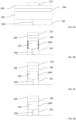
- FIG. 2A there Figure 2B , there Figure 2C , there 2D figure and the Figure 2E represent partial and schematic sectional views of successive steps of a method of manufacturing an electronic component according to one embodiment.
- the expressions “approximately”, “approximately”, “substantially”, and “of the order of” mean to within 10%, preferably to within 5%.
- FIG. 1A there Figure 1B , there Figure 1C and the Figure 1D represent partial and schematic sectional views of successive steps of an exemplary embodiment of a method for manufacturing a phase change memory cell.
- FIG. 1A illustrates a starting structure comprising an insulating layer 102 and a resistive heating element 102r also called “heater” in English, extending vertically in the insulating layer 102.
- the resistive element 102r is surrounded laterally by the insulating layer 102.
- the insulating layer 102 makes it possible, for example, to insulate and separate laterally the resistive element 102r from another neighboring resistive element 102r (not visible in the figures).
- the resistive element 102r is flush, by its upper face, with the upper face of the insulating layer 102, and, by its lower face, with the lower face of the insulating layer 102.
- the starting structure also includes a layer 104 made of a material based on germanium and an element from column sixteen of the periodic table.
- layer 104 is made of a chalcogenide material.
- layer 104 is made of a phase change material called PCM layer ("phase change material").
- PCM layer 104 is made of a material based on germanium and tellurium.
- the PCM layer 104 is made of a material based on germanium and selenium.
- the PCM layer 104 is based on an alloy of germanium, antimony and tellurium or GST (from the English "germanium antimony tellurium").
- layer 104 is made of an OTS material.
- the PCM layer 104 is, for example, formed on the upper face of the insulating layer 102 and the resistive element 102r.
- the PCM layer 104 is for example in contact, by its lower face, with the upper face of the insulating layer 102 and the resistive element 102r.
- the PCM layer 104 extends over the entire surface of the upper face of the insulating layer 102.
- the starting structure also comprises a conductive layer 106.
- the conductive layer 106 is, for example, formed on the upper face of the PCM layer 104.
- the conductive layer 106 is, for example, in contact, via its lower face, with the upper face of the PCM layer 104.
- the conductive layer 106 extends over the entire surface of the upper face of the PCM layer 104.
- the conductive layer 106 corresponds to the upper electrode of the memory cell formed during the following steps.
- the starting structure further comprises an insulating layer 108.
- the insulating layer 108 is, for example, formed on the upper face of the conductive layer 106.
- the insulating layer 108 is, for example, in contact, via its lower face, with the upper face of the conductive layer 106.
- the insulating layer 108 extends over the entire surface of the upper face of the conductive layer 106.
- the insulating layer 108 is, for example, covered by an etching mask 110.
- the etching mask 110 is, for example, formed on and in contact with the upper face of the insulating layer 108.
- the etching mask 110 does not, for example, extend over the entire surface of the upper face of the layer 108.
- the etching mask 110 is, for example, formed opposite the desired location for the memory cell.
- the stack formed by the layers 102, 104, 106, 108, 110 rests for example on and in contact with the upper face of a control integrated circuit, comprising one or more devices for selecting phase-change memory cells.
- the selection elements are transistors, diodes, or OTS elements.
- FIG. 1B illustrates a structure obtained at the end of an etching step of the stack formed by the insulating layer 102, the PCM layer 104, the conductive layer 106 and the insulating layer 108.
- the parts of the layers 102, 104, 106, 108 not protected by the etching mask 110 are removed.
- the etching of these layers comprises, among other things, a halogenated plasma etching step.
- the halogenated etching is carried out using hydrogen bromide (HBr), dichlorine (Cl 2 ), tetrafluoromethane (CF 4 ), fluoromethane (CF x , in which x is between 0.1 and 4).
- the PCM layer 104 has its sides 104f modified more than the layers 102, 106 and 108.
- the 104f sides of the PCM 104 layer are enriched with halogen atoms at its 104f sides.
- the PCM 104 layer is enriched over a thickness of between 1 nm and 20 nm, for example between 1 nm and 10 nm.
- the 104f sides of the PCM layer 104 comprise, at the end of this step, a percentage of halogen, for example in the first twenty nanometers, between 1% and 30%.
- the PCM 104 layer is made of a tellurium-based chalcogenide material
- the 104f sides of the PCM 104 layer are further enriched with tellurium.
- FIG. 1C illustrates a structure obtained at the end of a step of removing the etching mask 110.
- the removal of the mask 110 is for example carried out by an oxygen-based plasma etching step called “stripping”.
- the steps illustrated in Figures 1B and 1C are carried out under a pressure for example less than 100 Pa, for example less than 1 Pa.
- the steps of Figures 1B and 1C are carried out within the same equipment. For example, at the end of the step illustrated in Figure 1B , the structure is not put back into contact with oxygen before the step illustrated in Figure 1C .
- FIG. 1D illustrates a structure obtained at the end of a cleaning step of the structure illustrated in Figure 1C .
- the cleaning step illustrated in Figure 1D is for example carried out by a wet chemical treatment.
- cleaning is carried out using hydrofluoric acid and glycolic acid.
- This cleaning step is, for example, carried out while the structure has been exposed to air, i.e. it is carried out under atmospheric pressure and the structure is no longer under vacuum or inert atmosphere.
- the halogen atoms present in the 104f sides of the layer 104 are then degassed, that is to say they come out of the structure.
- the halogen atoms react with the air and form 104r residues on the surface of the 104f sides.
- the 104r residues can have dimensions of up to 300 nm, for example up to 200 nm.
- germanium oxide resulting from the reaction between the germanium present in the PCM layer 104, the surface of which has been altered during the cleaning step illustrated in Figure 1C , and oxygen present in the air, is further formed on the sides 104f of the PCM layer 104.
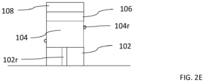
- FIG. 2A there Figure 2B , there Figure 2C , there 2D figure and the Figure 2E represent partial and schematic sectional views of successive steps of a method of manufacturing an electronic component according to one embodiment.
- FIG. 2A more particularly illustrates a starting structure identical to the starting structure illustrated in Figure 1A .
- the thickness of the PCM 104 layer is for example between 30 nm and 100 nm, for example between 40 nm and 60 nm.
- the conductive layer 106 is for example made of metal, for example a titanium-based alloy.
- the thickness of the conductive layer 106 is for example between 5 nm and 40 nm, for example between 15 nm and 30 nm.
- the insulating layer 108 is for example made of silicon nitride.
- the thickness of the insulating layer 108 is for example between 5 nm and 40 nm, for example between 15 nm and 30 nm.
- the mask 110 is for example made of carbon.
- the mask 110 has for example a thickness between 200 nm and 400 nm, for example between 250 nm and 300 nm.
- FIG. 2B illustrates a structure obtained at the end of an etching step of the stack formed by the insulating layer 102, the PCM layer 104, the conductive layer 106 and the insulating layer 108.
- This step is identical to that illustrated in Figure 1B
- this step is carried out in a capacitively coupled plasma (CCP) reactor or in an inductively coupled plasma (ICP) reactor.
- CCP capacitively coupled plasma
- ICP inductively coupled plasma
- FIG. 2C illustrates a structure obtained at the end of a step of processing the etched 104f sides of the PCM 104 layer. This step is carried out at the end of the step illustrated in Figure 2C without the structure being brought back into contact with oxygen.
- This step is performed by a hydrogen-based plasma.
- the plasma is composed of dihydrogen or ammonia, for example with one or more neutral gases such as argon or nitrogen.
- the neutral gases can, in the plasma, help with the ignition and stability of the plasma.
- the plasma used in this step does not include oxygen.
- the continuous or pulsed bias voltage applied to the plasma is relatively low, for example less than 100 V in absolute value.
- the continuous bias voltage is less than 10 V in absolute value.
- the continuous bias voltage is less than 1 V in absolute value.
- the continuous bias voltage is zero.
- This low bias value makes it possible in particular not to consume too large a quantity of the flanks 104f of the PCM layer 104.
- the polarization duty cycle i.e. the percentage of time during which the polarization voltage is applied to the substrate, is between 20% and 90% of the cycle time.
- the cycle frequency is between 100 Hz and 5 kHz.
- the flow of each gas in the plasma is between 25 cm 3 /min and 500 cm 3 /min.
- the power of the plasma source is between 200 W and 1000 W.
- the pressure applied in the reactor is between 3 mTorr (i.e. approximately 0.4 Pa) and 100 mTorr (i.e. approximately 13.3 Pa).
- the temperature of the structure is between 0 °C and 100 °C.
- this step has a duration of between 5 seconds and 30 seconds, for example between 5 and 15 seconds.
- the plasma allows a reduction in the percentage of tellurium in the PCM 104 layer, for example in a homogeneous manner in the entire PCM layer 104.
- this step further allows the cleaning of the sides of the conductive layer 106 on which halogen atoms can form residues during re-electroplating after the etching step illustrated in relation to the Figure 2B .
- FIG. 2D figure illustrates a structure obtained at the end of a step of removing the etching mask 110 from the structure illustrated in Figure 2C , for example identical to the step of removing the etching mask 110 illustrated in relation to the Figure 1C .
- the removal of the etching mask 110 is carried out during the step illustrated in relation to the Figure 2C by hydrogen plasma etching.
- FIG. 2E illustrates a structure obtained at the end of a cleaning step of the structure illustrated in 2D figure .
- This step is for example similar to the step illustrated in relation to the Figure 1D except that the sides 104f of the layer 104 of the structure illustrated in 2D figure have fewer halogen atoms than the 104f sides of the 104 layer of the structure illustrated in Figure 1D .
- residues 104r are then formed on the surface of the sides 104f of the PCM layer 104 but in a lesser proportion compared to the proportion of residues formed during the step illustrated in Figure 1D .
- step of treating the sides of the PCM layer by hydrogen plasma is performed between the halogen etching step and the step of removing the etching mask, it can be provided that it is performed after or during the step of removing the etching mask and before the structure is exposed to air.
- each cell comprises, above the conductive layer 106, a stack of a layer made of an OTS material and another conductive layer.
- the OTS layer is in contact, by its lower face with the upper face of the conductive layer 106 and the other conductive layer is in contact with the OTS layer.
Landscapes
- Engineering & Computer Science (AREA)
- Manufacturing & Machinery (AREA)
- Semiconductor Memories (AREA)
- Light Receiving Elements (AREA)
- Weting (AREA)
Applications Claiming Priority (1)
| Application Number | Priority Date | Filing Date | Title |
|---|---|---|---|
| FR2307957A FR3151702A1 (fr) | 2023-07-24 | 2023-07-24 | Procédé de fabrication d’un composant électronique |
Publications (1)
| Publication Number | Publication Date |
|---|---|
| EP4498786A1 true EP4498786A1 (de) | 2025-01-29 |
Family
ID=88839899
Family Applications (1)
| Application Number | Title | Priority Date | Filing Date |
|---|---|---|---|
| EP24189823.8A Withdrawn EP4498786A1 (de) | 2023-07-24 | 2024-07-19 | Verfahren zur herstellung eines elektronischen bauteils |
Country Status (3)
| Country | Link |
|---|---|
| US (1) | US20250040455A1 (de) |
| EP (1) | EP4498786A1 (de) |
| FR (1) | FR3151702A1 (de) |
Citations (3)
| Publication number | Priority date | Publication date | Assignee | Title |
|---|---|---|---|---|
| US20120091423A1 (en) * | 2010-10-14 | 2012-04-19 | Sony Corporation | Nonvolatile memory device and manufacturing method thereof |
| CN106252432A (zh) * | 2016-09-28 | 2016-12-21 | 中山瑞科新能源有限公司 | 一种可降低缺陷密度的碲化镉太阳能电池制备方法 |
| US20220344403A1 (en) * | 2021-04-23 | 2022-10-27 | Taiwan Semiconductor Manufacturing Company, Ltd. | Memory device, method of forming the same, and semiconductor device having the same |
-
2023
- 2023-07-24 FR FR2307957A patent/FR3151702A1/fr active Pending
-
2024
- 2024-07-19 EP EP24189823.8A patent/EP4498786A1/de not_active Withdrawn
- 2024-07-23 US US18/780,788 patent/US20250040455A1/en active Pending
Patent Citations (3)
| Publication number | Priority date | Publication date | Assignee | Title |
|---|---|---|---|---|
| US20120091423A1 (en) * | 2010-10-14 | 2012-04-19 | Sony Corporation | Nonvolatile memory device and manufacturing method thereof |
| CN106252432A (zh) * | 2016-09-28 | 2016-12-21 | 中山瑞科新能源有限公司 | 一种可降低缺陷密度的碲化镉太阳能电池制备方法 |
| US20220344403A1 (en) * | 2021-04-23 | 2022-10-27 | Taiwan Semiconductor Manufacturing Company, Ltd. | Memory device, method of forming the same, and semiconductor device having the same |
Also Published As
| Publication number | Publication date |
|---|---|
| FR3151702A1 (fr) | 2025-01-31 |
| US20250040455A1 (en) | 2025-01-30 |
Similar Documents
| Publication | Publication Date | Title |
|---|---|---|
| EP0351001B1 (de) | Verfahren zur Herstellung einer Halbleitervorrichtung mit mindestens einer kleine Kontaktlöcher enthaltenden Leiterbahn | |
| FR2508237A1 (fr) | Procede pour la fabrication d'une jonction de josephson, notamment d'une jonction tunnel de josephson | |
| EP0325808B1 (de) | Verfahren, um eine elektrische Verbindung auf einer Silizium-Halbleitervorrichtung herzustellen | |
| EP4000090B1 (de) | Verfahren zum hydrophilen zusammenfügen von substraten | |
| FR2981199A1 (fr) | Dispositif microelectronique a memoire programmable comportant une couche de chalcogenure dope resistante a des temperatures elevees | |
| FR3086462A1 (fr) | Procede de fabrication d'un composant electronique | |
| FR2641126A1 (en) | Method of forming low-resistance contacts with pre-ohmic regions of n<+> and p<+> types in integrated circuits | |
| WO2022008809A1 (fr) | Structure semi-conductrice comprenant une interface de collage electriquement conductrice, et procede de fabrication associe | |
| EP4498786A1 (de) | Verfahren zur herstellung eines elektronischen bauteils | |
| WO2015128399A2 (fr) | Procede de realisation d'une structure par assemblage d'au moins deux elements par collage direct | |
| FR2748601A1 (fr) | Procede de formation d'interconnexions dans un circuit integre | |
| EP2472624B1 (de) | Ätzverfahren für eine mikroelektronische programmierbare Speichervorrichtung | |
| EP1186024B1 (de) | Herstellungsverfahren für ein siliziumsubstrat mit einer dünnen, vergrabenen siliziumoxidschicht | |
| FR3043492A1 (fr) | Procede de fabrication de substrats | |
| EP4012735B1 (de) | Verfahren zur herstellung eines kondensators | |
| EP0336461B1 (de) | Planarisierungsverfahren der Oberflächen von Halbleiterbauelementen | |
| EP1540721B1 (de) | Verfahren zur Herstellung von Elektroden auf einem II-VI-Verbindungshalbleitermaterial | |
| EP3172357A1 (de) | Verfahren zur entfernung eines auf einer oberfläche in einer kammer aufgetragenen metallüberzugs | |
| EP4053884B1 (de) | Verfahren zum ätzen einer dielektrischen dreidimensionalen schicht | |
| EP4062463B1 (de) | Oxram-speicherzelle mit niedriger formbildungsspannung und zugehöriges herstellungsverfahren | |
| EP1396882A2 (de) | Verfahren zum Herstellen eines integrierten elektronischen Bauteils und elektrische Vorrichtung mit solchem Bauteil | |
| EP4053883B1 (de) | Verfahren zum ätzen einer dielektrischen dreidimensionalen schicht | |
| FR2485809A1 (fr) | Diode de type schottky aluminium-silicium, procede permettant sa fabrication et dispositif semi-conducteur comportant une telle diode | |
| EP2105959A2 (de) | Verfahren zur Bildung von mehrlagigen Verbindungen in einem integrierten Schaltkreis | |
| EP3414775B1 (de) | Verfahren zur herstellung vertikaler verbindungen auf einem chip |
Legal Events
| Date | Code | Title | Description |
|---|---|---|---|
| PUAI | Public reference made under article 153(3) epc to a published international application that has entered the european phase |
Free format text: ORIGINAL CODE: 0009012 |
|
| STAA | Information on the status of an ep patent application or granted ep patent |
Free format text: STATUS: REQUEST FOR EXAMINATION WAS MADE |
|
| 17P | Request for examination filed |
Effective date: 20240719 |
|
| AK | Designated contracting states |
Kind code of ref document: A1 Designated state(s): AL AT BE BG CH CY CZ DE DK EE ES FI FR GB GR HR HU IE IS IT LI LT LU LV MC ME MK MT NL NO PL PT RO RS SE SI SK SM TR |
|
| GRAP | Despatch of communication of intention to grant a patent |
Free format text: ORIGINAL CODE: EPIDOSNIGR1 |
|
| STAA | Information on the status of an ep patent application or granted ep patent |
Free format text: STATUS: GRANT OF PATENT IS INTENDED |
|
| RIC1 | Information provided on ipc code assigned before grant |
Ipc: H10B 63/10 20230101ALI20250521BHEP Ipc: H10B 63/00 20230101ALI20250521BHEP Ipc: H10N 70/20 20230101ALI20250521BHEP Ipc: H10N 70/00 20230101AFI20250521BHEP |
|
| INTG | Intention to grant announced |
Effective date: 20250616 |
|
| STAA | Information on the status of an ep patent application or granted ep patent |
Free format text: STATUS: THE APPLICATION IS DEEMED TO BE WITHDRAWN |
|
| 18D | Application deemed to be withdrawn |
Effective date: 20251017 |